EP0262575A2 - Couche interne autoalignée de prégauge d'ions mobiles pour la métallisation multicouche de circuits intégrés - Google Patents
Couche interne autoalignée de prégauge d'ions mobiles pour la métallisation multicouche de circuits intégrés Download PDFInfo
- Publication number
- EP0262575A2 EP0262575A2 EP87113918A EP87113918A EP0262575A2 EP 0262575 A2 EP0262575 A2 EP 0262575A2 EP 87113918 A EP87113918 A EP 87113918A EP 87113918 A EP87113918 A EP 87113918A EP 0262575 A2 EP0262575 A2 EP 0262575A2
- Authority
- EP
- European Patent Office
- Prior art keywords
- layer
- metal
- composition
- gettering
- depositing
- Prior art date
- Legal status (The legal status is an assumption and is not a legal conclusion. Google has not performed a legal analysis and makes no representation as to the accuracy of the status listed.)
- Granted
Links
Images
Classifications
-
- H10W74/43—
-
- H10P14/412—
-
- H10W20/063—
-
- H10W20/064—
-
- H10W20/425—
-
- H10W20/4432—
-
- H10W74/137—
Definitions
- This invention relates generally to a method of making and a structure of a gate and interconnect metallization for an integrated circuit device and more particularly to a multi-layer metallization method and structure.
- Multi-layer metallization structures are discussed in J. L. Vossen, "VLSI Metallization Problems and Trends," Semiconductor International, Sept. 1981, pages 91-99 and in S.M. Sze, "VLSI Technology,” 1983, pages 360-372. Many variations have been suggested.
- One multi-layer metallization structure of particular interest conventionally comprises a conductor of a noble metal, such as gold, with a barrier layer of a refractory metal, such as titanium-tungsten, deposited between the conductor metal and the substrate surface.
- barrier metallization is to inhibit diffusion of the gold into the substrate, typically silicon, and formation of an eutectic that impairs the semiconductive properties of the substrate material.
- Conventional metallization processes include forming an oxide (SiO2) layer on the silicon substrate, forming contact openings in the oxide layer over semiconductor devices formed in the substrate, sputter-depositing a layer of titanium-tungsten onto the substrate surface, patterning the barrier metallization, and gold plating the conductor metal onto the barrier metal.
- oxide SiO2
- An example of such processes is detailed in D. Summers, "A Process for Two-Layer Gold IC Metallization," Solid State Technology, pages 137-141, Dec. 1983.
- Field threshold voltage is the static voltage required between an electrode contacting the field oxide and the underlying semiconductor substrate (i.e., across the field oxide) to invert the underlying region of a doped semiconductor substrate from one type (e.g., p-type) to the other (e.g., n-type). In MOS technology this corresponds to gate threshold voltage, V t .
- One problem with gate metallization structures as described above is that the circuit devices frequently exhibit a large field threshold voltage shift.
- the measurement of field threshold voltage shift is conventionally expressed in terms of a shift of flat band voltage in millivolts per thousand angstroms of field oxide thickness.
- a typical inversion voltage for a bipolar integrated circuit fabricated on a doped silicon substrate is in the range of 20-25 volts for a field oxide thickness of about 1 micron. In cases of mobile sodium ion contamination, within the field oxide, this voltage can shift downward 10 volts or more (1 volt/1000 ⁇ ), causing device isolation within the substrate to fail. An acceptable amount of voltage shift is normally 5 volts or less (under 500 millivolts/1000 ⁇ of field oxide thickness).
- titanium-tungsten barrier metal is a major contributor of the field oxide sodium ions.
- PSG phosphorus silicate glass
- a need remains for a multi-layer metallization structure and method that will permit the use of a barrier metal such as titanium-tungsten that may be contaminated with metal ions, particularly sodium, without degrading operating characteristics of the integrated circuit.
- One object of the invention is to improve upon prior methods of metallization that employ a barrier metal in contact with the substrate surface.
- a second object of the invention is to minimize the effects on integrated circuit operating characteristics, particularly field threshold voltage shift, that occur in connection with the use of barrier metal layers.
- Another object of the invention is to minimize further complication of integrated circuit fabrication processes, particularly avoiding additional photolithography steps.
- a further object of the invention is to provide a metallization method that is compatible with the conventional integrated circuit fabrication processes.
- the invention provides a multilayer metallization method and structure for an integrated circuit that permits the use of a metal-ion contaminated refractory metal, e.g., titanium-tungsten (Ti:W) with sodium ions (Na+), without significant degradation of device characteristics.
- a metal-ion contaminated refractory metal e.g., titanium-tungsten (Ti:W) with sodium ions (Na+)
- a layer of a gettering composition preferably phosphorous silicate glass
- the gettering composition is then selectively removed, e.g., by reactive ion etching, to expose the field oxide and top surface of the conductor metal, while leaving a gettering composition layer on each sidewall of the metallization structure.
- the circuit is then annealed at a temperature and for a duration sufficient to mobilize and transfer metal ions from the barrier metal and adjoining field oxide-substrate regions into the gettering composition.
- an adhesion layer and an insulative layer e.g., silicon dioxide are deposited over the metallization structure and field oxide, with the adhesion layer in the exposed top surface of the conductor metal and the gettering composition.
- the resultant circuit has electrical characteristics, such as field threshold voltage shift, comparable to devices made without a metal-ion-contaminated barrier layer. Moreover, the resultant structure retains the gettering composition layers in contact with the metallization sidewalls notwithstanding poor adhesion between them.
- sidewall structures have previously been used in integrated circuits (Park, et al., U.S. Pat. No. 4,477,310) such structures are not of compositions used in the present invention and do not pertain to the problems, objectives and solutions of the present invention.
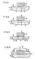
- an integrated circuit is conventionally formed on a silicon substrate 10 with a field oxide (SiO2) layer 12 covering the substrate in field areas between circuit device regions (not shown) implanted or diffused into the silicon.
- Layer 12 serves to insulate the semiconductive material 10 from conductors to be formed on its surface 13 as described below.
- Contact openings (not shown) for the conductors to contact the substrate material 10 are formed in the field oxide layer 12 in positions aligned with gate, source and drain (or base, collector, and emitter) regions of each circuit device.
- the field oxide layer is suitably of a thickness of 2,000-9,000 ⁇ and can be formed by either thermal oxidation or other known SiO2 deposition techniques.
- barrier metal is deposited onto substrate surface 13.
- Various refractory metal compositions containing titanium-tungsten (Ti:W) and other metals in varying proportions are conventionally used.
- the barrier metal is suitably deposited to a thickness of about 1,250 ⁇ .
- the barrier metal is sputter-deposited onto the substrate surface from a sputtering target formed of the desired titanium-tungsten composition.
- targets conventionally contain minute amounts of contaminant metal ions, such as sodium, that are also transferred to the deposition layer by the sputtering process. In accordance with the invention, such targets can be used.
- the barrier metal need not be devoid of contaminant metals, but can contain such amounts of contaminant metal ions including sodium as are found in commercially available titanium-tungsten barrier metal targets (e.g., sodium concentrations of 3-10 parts per million per manufacturer's specifications).
- the barrier metal layer is patterned using conventional photolithographic techniques.
- a conductor metal layer 16 is deposited by electroplating onto the barrier metal layer 14.
- the electroplated metal is deposited only in the open areas (i.e., non-photoresist-covered) of the patterned substrate.
- the plated metal thus defines a predetermined network of contacts and interconnects between the various devices in the integrated circuit.
- the photoresist is then stripped and the wafer is etched to remove the barrier metal from the field regions between the plated conductor metal.
- the etching step etches away the edges of the barrier metal layer 14 to produce a slight recess 15 beneath the sidewalls of the conductor metal layer 16.
- Various metals can be used for the conductor metal but a noble metal, such as gold, is preferred.
- the gold layer is deposited to a thickness of about 8,000 ⁇ .
- a layer 18 of a gettering composition is deposited over the entire substrate, including the sidewalls of the barrier and conductor metal layers 14, 16.
- the gettering composition is selected for its ability to getter undesired contaminant ions that are present in the barrier metal deposited in layer 14.
- the preferred gettering composition is 4% to 8%-by-weight phosphorous-silicate glass (PSG).
- PSG phosphorous-silicate glass
- Other compositions, such as arsenosilicate glass may also be suitable for this purpose.
- the phosphorous-silicate glass is chemical vapor deposited onto the substrate and metallization layers.
- gettering composition layer 18 is etched anisotropically using fluorocarbon-based reactive-ion etching (RIE) to remove portions of such layer that extend parallel to the substrate surface. This is done to selectively expose the top surface of the conductor metal 16 and the surface 13 of the field oxide layer while leaving sidewall layers 18a on both sides of the metallization structure 14, 16.
- RIE reactive-ion etching
- the metallization structure as actually fabricated and appearing in cross section in photomicrographs reveals a more rounded shape, in which the PSG sidewall layers 18a are crescent shaped, with one end contacting both the edge 15 of the barrier metal layer 14 and the surface 13 of the field oxide.
- the structure fabricated in FIGS. 1 and 2 is subjected to a heat treatment or annealing step.
- Annealing at sufficient temperature mobilizes any contaminant sodium ions in the barrier metal and causes such ions to out-diffuse into adjacent materials, including the gettering composition, where they react and bond within the gettering medium.
- a substantial proportion of the sodium ions, that would otherwise diffuse into the field oxide layer and migrate during circuit operation to the field oxide-silicon interface, are thus absorbed by the gettering composition.
- the annealing temperature must not be so high as to damage the circuit but may otherwise be within the ranges of temperature ordinarily used in processing integrated circuits.
- This temperature can strictly not be much above 400°C for gold metallization, but can be higher for the other conductor metals.
- annealing a chip containing the above-described gold/Ti:W/PSG structure at about 400°C for about 30 minutes is sufficient to out-diffuse a sufficient amount of mobile contaminant metal ions (Na+) from the barrier metal layer 14 and adjoining portions of the field oxide 12 to obtain a field voltage shift within acceptable limits (less than 500 millivolts per 1000 ⁇ of field oxide thickness).
- Annealing need not be performed as a separate step if subsequent processing of the integrated circuit includes annealing at about 400°C or more and for about 30 minutes or longer.
- a layer 22 of silicon nitride (Si3N4) is deposited by plasma enhanced chemical vapor deposition over the field oxide, the PSG sidewall layers 18a and the exposed top surface of the gold layer 16.
- Layer 22 is deposited to a thickness in the range of 170-270 ⁇ , and preferably of about 250 ⁇ .
- Silicon nitride is itself insulative, but is primarily provided as an adhesion layer.
- an insulative oxide (SiO2) layer 24 is deposited over the nitride layer 22.
- the oxide layer is preferably deposited by plasma enhanced chemical vapor deposition to a thickness of about 7,500 ⁇ .
- Tests of integrated circuits constructed as described above have demonstrated a significant reduction of field voltage shift from similarly-constructed circuits without the gettering composition sidewall layers.
- the non-gettered structure had an average field threshold voltage shift of 1.4 volts per 1000 ⁇ , and a range of 1.17 to 2.16 volts per 1000 ⁇ .
- Test circuits identically fabricated except using the gettering-metallization structure of the invention exhibited an average field threshold voltage shift of 380 millivolts per 1000 ⁇ of oxide thickness and a range of 270 to 480 millivolts per 1000 ⁇ . For a field oxide thickness of 9000 ⁇ , this range typically provides an inversion voltage greater than 15 volts.
- the method of the invention provides easy self-alignment of the gettering material with the major source of mobile ion contamination (i.e., the barrier metal), requires no additional photolithography and is compatible with prior, conventional integrated circuit processes. Moreover, it makes possible extending conventional metallization methods to new families of devices, such as CMOS integrated circuitry.
Landscapes
- Internal Circuitry In Semiconductor Integrated Circuit Devices (AREA)
- Electrodes Of Semiconductors (AREA)
- Local Oxidation Of Silicon (AREA)
Applications Claiming Priority (2)
| Application Number | Priority Date | Filing Date | Title |
|---|---|---|---|
| US915303 | 1986-10-03 | ||
| US06/915,303 US4732865A (en) | 1986-10-03 | 1986-10-03 | Self-aligned internal mobile ion getter for multi-layer metallization on integrated circuits |
Publications (3)
| Publication Number | Publication Date |
|---|---|
| EP0262575A2 true EP0262575A2 (fr) | 1988-04-06 |
| EP0262575A3 EP0262575A3 (en) | 1989-01-18 |
| EP0262575B1 EP0262575B1 (fr) | 1993-02-10 |
Family
ID=25435531
Family Applications (1)
| Application Number | Title | Priority Date | Filing Date |
|---|---|---|---|
| EP87113918A Expired - Lifetime EP0262575B1 (fr) | 1986-10-03 | 1987-09-23 | Couche interne autoalignée de prégauge d'ions mobiles pour la métallisation multicouche de circuits intégrés |
Country Status (4)
| Country | Link |
|---|---|
| US (1) | US4732865A (fr) |
| EP (1) | EP0262575B1 (fr) |
| JP (1) | JPS63172448A (fr) |
| DE (1) | DE3784124T2 (fr) |
Cited By (4)
| Publication number | Priority date | Publication date | Assignee | Title |
|---|---|---|---|---|
| GB2211349A (en) * | 1987-10-22 | 1989-06-28 | Mitsubishi Electric Corp | Method of producing a gate electrode |
| EP0601723A3 (fr) * | 1992-11-24 | 1995-05-17 | American Telephone & Telegraph | Procédé de fabrication de circuit intégré. |
| US5920794A (en) * | 1994-02-18 | 1999-07-06 | Telefonaktiebolaget Lm Ericsson | Electromigration resistant metallization process microcircuit interconnections with RF-reactively sputtered titanium tungsten and gold |
| US6653732B2 (en) | 2000-05-05 | 2003-11-25 | Infineon Technologies Ag | Electronic component having a semiconductor chip |
Families Citing this family (21)
| Publication number | Priority date | Publication date | Assignee | Title |
|---|---|---|---|---|
| US4927505A (en) * | 1988-07-05 | 1990-05-22 | Motorola Inc. | Metallization scheme providing adhesion and barrier properties |
| US4880708A (en) * | 1988-07-05 | 1989-11-14 | Motorola, Inc. | Metallization scheme providing adhesion and barrier properties |
| US4980301A (en) * | 1988-12-21 | 1990-12-25 | At&T Bell Laboratories | Method for reducing mobile ion contamination in semiconductor integrated circuits |
| US5227314A (en) * | 1989-03-22 | 1993-07-13 | At&T Bell Laboratories | Method of making metal conductors having a mobile inn getterer therein |
| US5016081A (en) * | 1989-03-22 | 1991-05-14 | At&T Bell Laboratories | Mobile ion getterer for metal conductors |
| US5195017A (en) * | 1989-12-13 | 1993-03-16 | Texas Instruments Incorporated | Method for forming a polysilicon to polysilicon capacitor and apparatus formed therefrom |
| US5866937A (en) * | 1990-04-12 | 1999-02-02 | Actel Corporation | Double half via antifuse |
| US5780323A (en) * | 1990-04-12 | 1998-07-14 | Actel Corporation | Fabrication method for metal-to-metal antifuses incorporating a tungsten via plug |
| US5614756A (en) * | 1990-04-12 | 1997-03-25 | Actel Corporation | Metal-to-metal antifuse with conductive |
| US5134539A (en) * | 1990-12-17 | 1992-07-28 | Nchip, Inc. | Multichip module having integral decoupling capacitor |
| US5214844A (en) * | 1990-12-17 | 1993-06-01 | Nchip, Inc. | Method of assembling integrated circuits to a silicon board |
| US5274270A (en) * | 1990-12-17 | 1993-12-28 | Nchip, Inc. | Multichip module having SiO2 insulating layer |
| TW274628B (fr) * | 1994-06-03 | 1996-04-21 | At & T Corp | |
| US5789764A (en) * | 1995-04-14 | 1998-08-04 | Actel Corporation | Antifuse with improved antifuse material |
| EP0774164A1 (fr) * | 1995-06-02 | 1997-05-21 | Actel Corporation | Antifusible a plot en tungstene sureleve et procede de fabrication |
| US5913131A (en) * | 1996-11-14 | 1999-06-15 | Advanced Micro Devices, Inc. | Alternative process for BPTEOS/BPSG layer formation |
| KR100241506B1 (ko) * | 1997-06-23 | 2000-03-02 | 김영환 | 반도체 소자의 금속 배선 형성 방법 |
| US20100044804A1 (en) * | 2008-08-25 | 2010-02-25 | Taiwan Semiconductor Manufacturing Company, Ltd. | Novel high-k metal gate structure and method of making |
| US8518818B2 (en) | 2011-09-16 | 2013-08-27 | Taiwan Semiconductor Manufacturing Co., Ltd. | Reverse damascene process |
| US9070854B2 (en) * | 2012-04-27 | 2015-06-30 | Varian Semiconductor Equipment Associates, Inc. | Techniques for patterning multilayer magnetic memory devices using ion implantation |
| RU2611098C1 (ru) * | 2015-12-09 | 2017-02-21 | Акционерное общество "Научно-исследовательский институт молекулярной электроники" | Способ формирования системы многоуровневой металлизации на основе вольфрама для высокотемпературных интегральных микросхем |
Family Cites Families (4)
| Publication number | Priority date | Publication date | Assignee | Title |
|---|---|---|---|---|
| US4485550A (en) * | 1982-07-23 | 1984-12-04 | At&T Bell Laboratories | Fabrication of schottky-barrier MOS FETs |
| US4477310A (en) * | 1983-08-12 | 1984-10-16 | Tektronix, Inc. | Process for manufacturing MOS integrated circuit with improved method of forming refractory metal silicide areas |
| US4589928A (en) * | 1984-08-21 | 1986-05-20 | At&T Bell Laboratories | Method of making semiconductor integrated circuits having backside gettered with phosphorus |
| DE3583472D1 (de) * | 1984-08-28 | 1991-08-22 | Toshiba Kawasaki Kk | Verfahren zum herstellen einer halbleiteranordnung mit gateelektrode. |
-
1986
- 1986-10-03 US US06/915,303 patent/US4732865A/en not_active Expired - Fee Related
-
1987
- 1987-09-23 EP EP87113918A patent/EP0262575B1/fr not_active Expired - Lifetime
- 1987-09-23 DE DE8787113918T patent/DE3784124T2/de not_active Expired - Fee Related
- 1987-10-02 JP JP62249667A patent/JPS63172448A/ja active Granted
Non-Patent Citations (3)
| Title |
|---|
| JOURNAL OF THE ELECTROCHEMICAL SOCIETY, vol. 133, no. 2, February 1986, pages 401-407, Manchester, New Hampshire, US; N. YAMAMOTO et al.: "Fabrication of highly reliable tungsten gate MOS VLSI's" * |
| PROCEEDINGS OF THE IEEE, vol. 57, no. 9, September 1969, pages 1558-1563; P. BALK et al.: "Phosphosilicate glass stabilization of FET devices" * |
| SOLID STATE TECHNOLOGY, vol. 26, no. 12, December 1983, pages 137-141; D. SUMMERS: "A process for two-layer gold IC metallization" * |
Cited By (6)
| Publication number | Priority date | Publication date | Assignee | Title |
|---|---|---|---|---|
| GB2211349A (en) * | 1987-10-22 | 1989-06-28 | Mitsubishi Electric Corp | Method of producing a gate electrode |
| US5030589A (en) * | 1987-10-22 | 1991-07-09 | Mitsubishi Denki Kabushiki Kaisha | Production method for a semiconductor device |
| EP0601723A3 (fr) * | 1992-11-24 | 1995-05-17 | American Telephone & Telegraph | Procédé de fabrication de circuit intégré. |
| US5920794A (en) * | 1994-02-18 | 1999-07-06 | Telefonaktiebolaget Lm Ericsson | Electromigration resistant metallization process microcircuit interconnections with RF-reactively sputtered titanium tungsten and gold |
| US6211568B1 (en) | 1994-02-18 | 2001-04-03 | Telefonaktiebolaget Lm Ericsson(Publ) | Electromigration resistant metallization structures and process for microcircuit interconnections with RF-reactively sputtered titanium tungsten and gold |
| US6653732B2 (en) | 2000-05-05 | 2003-11-25 | Infineon Technologies Ag | Electronic component having a semiconductor chip |
Also Published As
| Publication number | Publication date |
|---|---|
| EP0262575B1 (fr) | 1993-02-10 |
| DE3784124T2 (de) | 1993-09-16 |
| EP0262575A3 (en) | 1989-01-18 |
| DE3784124D1 (de) | 1993-03-25 |
| JPH0444415B2 (fr) | 1992-07-21 |
| JPS63172448A (ja) | 1988-07-16 |
| US4732865A (en) | 1988-03-22 |
Similar Documents
| Publication | Publication Date | Title |
|---|---|---|
| EP0262575A2 (fr) | Couche interne autoalignée de prégauge d'ions mobiles pour la métallisation multicouche de circuits intégrés | |
| US4392150A (en) | MOS Integrated circuit having refractory metal or metal silicide interconnect layer | |
| KR890004463B1 (ko) | 금속 전극 배선막을 가진 반도체 장치 | |
| EP0435388B1 (fr) | Procédé pour remplir sélectivement des contacts ou des passages de profondeurs différente | |
| US4648175A (en) | Use of selectively deposited tungsten for contact formation and shunting metallization | |
| US5342806A (en) | Method for fabricating a semiconductor device having a conductor structure with a plated layer | |
| EP0236034A2 (fr) | Déposition sélective sans électricité de circuits de transits dans des dispositifs VLSI | |
| US3918149A (en) | Al/Si metallization process | |
| EP0055521B1 (fr) | Procédé de remplissage d'une rainure dans un substrat semiconducteur | |
| EP0076105B1 (fr) | Procédé de fabrication d'un transitor bipolair | |
| US4961822A (en) | Fully recessed interconnection scheme with titanium-tungsten and selective CVD tungsten | |
| EP0018175B1 (fr) | Procédé pour la fabrication d'une électrode sur un dispositif semiconducteur | |
| EP0318954A2 (fr) | Dispositif semi-conducteur comprenant une couche intermédiaire composée en matière isolante | |
| EP0426305A1 (fr) | Méthode pour attaquer des fenêtres de différentes profondeurs | |
| US4525733A (en) | Patterning method for reducing hillock density in thin metal films and a structure produced thereby | |
| US4981816A (en) | MO/TI Contact to silicon | |
| GB2128636A (en) | Silicon-aluminium alloy metallization of semiconductor substrate | |
| JPS6364057B2 (fr) | ||
| KR19990028850A (ko) | 두꺼운 도체를 갖는 모노리식 마이크로파 회로를 제조하는 방법 | |
| KR910006975B1 (ko) | 도전성 플러그로 집적 회로 상의 접점 및 비아를 충전하는 방법 | |
| EP0514103A1 (fr) | Procédé de fabrication d'une barrière en métal pour contacts sous-micromiques | |
| EP0660392A1 (fr) | Méthode et structure du diélectrique intercouche pour un meilleur recouvrement métallique de marche | |
| US5212150A (en) | Oxide superconducting lead for interconnecting device component with a semiconductor substrate via at least one buffer layer | |
| JPH10229086A (ja) | 半導体装置およびその製造方法 | |
| US5136361A (en) | Stratified interconnect structure for integrated circuits |
Legal Events
| Date | Code | Title | Description |
|---|---|---|---|
| PUAI | Public reference made under article 153(3) epc to a published international application that has entered the european phase |
Free format text: ORIGINAL CODE: 0009012 |
|
| AK | Designated contracting states |
Kind code of ref document: A2 Designated state(s): DE FR GB NL |
|
| PUAL | Search report despatched |
Free format text: ORIGINAL CODE: 0009013 |
|
| AK | Designated contracting states |
Kind code of ref document: A3 Designated state(s): DE FR GB NL |
|
| 17P | Request for examination filed |
Effective date: 19890622 |
|
| 17Q | First examination report despatched |
Effective date: 19910403 |
|
| RAP1 | Party data changed (applicant data changed or rights of an application transferred) |
Owner name: TEKTRONIX, INC. |
|
| GRAA | (expected) grant |
Free format text: ORIGINAL CODE: 0009210 |
|
| AK | Designated contracting states |
Kind code of ref document: B1 Designated state(s): DE FR GB NL |
|
| PG25 | Lapsed in a contracting state [announced via postgrant information from national office to epo] |
Ref country code: FR Free format text: THE PATENT HAS BEEN ANNULLED BY A DECISION OF A NATIONAL AUTHORITY Effective date: 19930210 |
|
| REF | Corresponds to: |
Ref document number: 3784124 Country of ref document: DE Date of ref document: 19930325 |
|
| ET | Fr: translation filed | ||
| PG25 | Lapsed in a contracting state [announced via postgrant information from national office to epo] |
Ref country code: GB Effective date: 19930923 |
|
| PLBE | No opposition filed within time limit |
Free format text: ORIGINAL CODE: 0009261 |
|
| STAA | Information on the status of an ep patent application or granted ep patent |
Free format text: STATUS: NO OPPOSITION FILED WITHIN TIME LIMIT |
|
| 26N | No opposition filed | ||
| PG25 | Lapsed in a contracting state [announced via postgrant information from national office to epo] |
Ref country code: NL Effective date: 19940401 |
|
| NLV4 | Nl: lapsed or anulled due to non-payment of the annual fee | ||
| GBPC | Gb: european patent ceased through non-payment of renewal fee |
Effective date: 19930923 |
|
| REG | Reference to a national code |
Ref country code: FR Ref legal event code: ST |
|
| PGFP | Annual fee paid to national office [announced via postgrant information from national office to epo] |
Ref country code: DE Payment date: 19940824 Year of fee payment: 8 |
|
| PG25 | Lapsed in a contracting state [announced via postgrant information from national office to epo] |
Ref country code: DE Effective date: 19960601 |