EP0262284A1 - Connection apparatus for integrated circuit - Google Patents
Connection apparatus for integrated circuit Download PDFInfo
- Publication number
- EP0262284A1 EP0262284A1 EP87101550A EP87101550A EP0262284A1 EP 0262284 A1 EP0262284 A1 EP 0262284A1 EP 87101550 A EP87101550 A EP 87101550A EP 87101550 A EP87101550 A EP 87101550A EP 0262284 A1 EP0262284 A1 EP 0262284A1
- Authority
- EP
- European Patent Office
- Prior art keywords
- circuit board
- substrate
- main face
- face
- aperture
- Prior art date
- Legal status (The legal status is an assumption and is not a legal conclusion. Google has not performed a legal analysis and makes no representation as to the accuracy of the status listed.)
- Granted
Links
Images
Classifications
-
- H—ELECTRICITY
- H05—ELECTRIC TECHNIQUES NOT OTHERWISE PROVIDED FOR
- H05K—PRINTED CIRCUITS; CASINGS OR CONSTRUCTIONAL DETAILS OF ELECTRIC APPARATUS; MANUFACTURE OF ASSEMBLAGES OF ELECTRICAL COMPONENTS
- H05K7/00—Constructional details common to different types of electric apparatus
- H05K7/02—Arrangements of circuit components or wiring on supporting structure
- H05K7/10—Plug-in assemblages of components, e.g. IC sockets
- H05K7/1053—Plug-in assemblages of components, e.g. IC sockets having interior leads
- H05K7/1061—Plug-in assemblages of components, e.g. IC sockets having interior leads co-operating by abutting
-
- H—ELECTRICITY
- H05—ELECTRIC TECHNIQUES NOT OTHERWISE PROVIDED FOR
- H05K—PRINTED CIRCUITS; CASINGS OR CONSTRUCTIONAL DETAILS OF ELECTRIC APPARATUS; MANUFACTURE OF ASSEMBLAGES OF ELECTRICAL COMPONENTS
- H05K1/00—Printed circuits
- H05K1/02—Details
- H05K1/0201—Thermal arrangements, e.g. for cooling, heating or preventing overheating
- H05K1/0203—Cooling of mounted components
- H05K1/0204—Cooling of mounted components using means for thermal conduction connection in the thickness direction of the substrate
-
- H—ELECTRICITY
- H10—SEMICONDUCTOR DEVICES; ELECTRIC SOLID-STATE DEVICES NOT OTHERWISE PROVIDED FOR
- H10W—GENERIC PACKAGES, INTERCONNECTIONS, CONNECTORS OR OTHER CONSTRUCTIONAL DETAILS OF DEVICES COVERED BY CLASS H10
- H10W70/00—Package substrates; Interposers; Redistribution layers [RDL]
- H10W70/60—Insulating or insulated package substrates; Interposers; Redistribution layers
- H10W70/67—Insulating or insulated package substrates; Interposers; Redistribution layers characterised by their insulating layers or insulating parts
- H10W70/68—Shapes or dispositions thereof
-
- H—ELECTRICITY
- H05—ELECTRIC TECHNIQUES NOT OTHERWISE PROVIDED FOR
- H05K—PRINTED CIRCUITS; CASINGS OR CONSTRUCTIONAL DETAILS OF ELECTRIC APPARATUS; MANUFACTURE OF ASSEMBLAGES OF ELECTRICAL COMPONENTS
- H05K1/00—Printed circuits
- H05K1/18—Printed circuits structurally associated with non-printed electric components
- H05K1/182—Printed circuits structurally associated with non-printed electric components associated with components mounted in printed circuit boards [PCB], e.g. insert-mounted components [IMC]
-
- H—ELECTRICITY
- H05—ELECTRIC TECHNIQUES NOT OTHERWISE PROVIDED FOR
- H05K—PRINTED CIRCUITS; CASINGS OR CONSTRUCTIONAL DETAILS OF ELECTRIC APPARATUS; MANUFACTURE OF ASSEMBLAGES OF ELECTRICAL COMPONENTS
- H05K2201/00—Indexing scheme relating to printed circuits covered by H05K1/00
- H05K2201/10—Details of components or other objects attached to or integrated in a printed circuit board
- H05K2201/10227—Other objects, e.g. metallic pieces
- H05K2201/10409—Screws
-
- H—ELECTRICITY
- H05—ELECTRIC TECHNIQUES NOT OTHERWISE PROVIDED FOR
- H05K—PRINTED CIRCUITS; CASINGS OR CONSTRUCTIONAL DETAILS OF ELECTRIC APPARATUS; MANUFACTURE OF ASSEMBLAGES OF ELECTRICAL COMPONENTS
- H05K2201/00—Indexing scheme relating to printed circuits covered by H05K1/00
- H05K2201/10—Details of components or other objects attached to or integrated in a printed circuit board
- H05K2201/10227—Other objects, e.g. metallic pieces
- H05K2201/10416—Metallic blocks or heatsinks completely inserted in a PCB
-
- H—ELECTRICITY
- H05—ELECTRIC TECHNIQUES NOT OTHERWISE PROVIDED FOR
- H05K—PRINTED CIRCUITS; CASINGS OR CONSTRUCTIONAL DETAILS OF ELECTRIC APPARATUS; MANUFACTURE OF ASSEMBLAGES OF ELECTRICAL COMPONENTS
- H05K2201/00—Indexing scheme relating to printed circuits covered by H05K1/00
- H05K2201/10—Details of components or other objects attached to or integrated in a printed circuit board
- H05K2201/10613—Details of electrical connections of non-printed components, e.g. special leads
- H05K2201/10621—Components characterised by their electrical contacts
- H05K2201/10727—Leadless chip carrier [LCC], e.g. chip-modules for cards
-
- H—ELECTRICITY
- H05—ELECTRIC TECHNIQUES NOT OTHERWISE PROVIDED FOR
- H05K—PRINTED CIRCUITS; CASINGS OR CONSTRUCTIONAL DETAILS OF ELECTRIC APPARATUS; MANUFACTURE OF ASSEMBLAGES OF ELECTRICAL COMPONENTS
- H05K3/00—Apparatus or processes for manufacturing printed circuits
- H05K3/30—Assembling printed circuits with electric components, e.g. with resistors
- H05K3/32—Assembling printed circuits with electric components, e.g. with resistors electrically connecting electric components or wires to printed circuits
- H05K3/325—Assembling printed circuits with electric components, e.g. with resistors electrically connecting electric components or wires to printed circuits by abutting or pinching; Mechanical auxiliary parts therefor
-
- H—ELECTRICITY
- H10—SEMICONDUCTOR DEVICES; ELECTRIC SOLID-STATE DEVICES NOT OTHERWISE PROVIDED FOR
- H10W—GENERIC PACKAGES, INTERCONNECTIONS, CONNECTORS OR OTHER CONSTRUCTIONAL DETAILS OF DEVICES COVERED BY CLASS H10
- H10W90/00—Package configurations
- H10W90/701—Package configurations characterised by the relative positions of pads or connectors relative to package parts
- H10W90/751—Package configurations characterised by the relative positions of pads or connectors relative to package parts of bond wires
- H10W90/754—Package configurations characterised by the relative positions of pads or connectors relative to package parts of bond wires between a chip and a stacked insulating package substrate, interposer or RDL
Definitions
- This invention relates to connection apparatus for integrated circuits.
- U.S. Patent No. 4,255,003 discloses a device for connecting a monolithic integrated circuit to a circuit board.
- the monolithic integrated circuit is mounted on a rectangular ceramic substrate that has connection pads distributed about the periphery of one main face of the substrate.
- the circuit board has corresponding connection pads exposed at one main face of the board about the periphery of a rectangular "footprint" region corresponding in shape and size to the main face of the ceramic substrate.
- the circuit board is formed with holes outside the footprint region.
- a clamping member has four rigid side portions that are connected together and form a rectangular frame. The side portions are formed with an endless groove at the underside of the frame.
- a frame-like body of elastomeric material projects downwardly from the underside of the clamping member and has a locating ridge that fits in the groove of the clamping member.
- Strips of conductive material are bonded to the underside of the body of elastomeric material.
- the elastomeric material is silicone rubber.
- the clamping member has an ear that extends downwardly somewhat beyond the underside of the frame, and each ear is formed with a hole.
- the circuit board is formed with corresponding holes. Through use of screws extending downwardly through the holes in the ears and the corresponding holes in the circuit board, and nuts engaging the lower ends of the screws, the clamping member may be attached to the circuit board.
- the elastomeric material When the clamping member is so attached, the elastomeric material is compressed and the strips of conductive material provide electrical connection between the connection pads of the substrate and the corresponding connection pads of the circuit board. The compression of the elastomeric material provides contact force between the strips of conductive material and the contact pads.
- a practical implementation of the conventional connection device disclosed in Patent No. 4,255,003 is designed for use with a substrate that is about 0.64 mm thick.
- the underside of the frame is stepped, in that the lower surface portion that is inward of the groove is at a height of 1.45 mm above the bottom of the ears and the lower surface portion that is outward of the groove is at a height of 0.81 mm above the bottom of the ears.
- the body of elastomeric material has two lobes, for engaging the substrate and the circuit board respectively, and each extends 1.02 mm downwards from the relevant surface portion of the frame.
- each lobe When the clamping member is attached to the circuit board and the screws are tightened, each lobe is compressed to a thickness of 0.81 mm, so that the percentage compression of each lobe is about 20%.
- manufacturing tolerances result in the percentage compression of the lobes possibly being different from 20%. Nevertheless, the tolerances are sufficiently small, e.g. ⁇ 0.05 mm on each component, that for all values of the percentage compression permitted by the manufacturing tolerances, adequate contact force is pro vided between the conductive strips and the pads of the substrate.
- the main mechanism for dissipation of heat from the integrated circuit is by conduction downwards through the ceramic substrate into the circuit board. Heat is removed from the bottom face of the circuit board by convection and/or conduction.
- Circuit board material e.g. epoxy glass
- the practical implementation of the conventional connection device is designed for use with circuit boards no thicker than about 0.64 mm, i.e. single layer circuit boards. It is, however, desirable to be able to use multilayer circuit boards that are about 1.57 mm thick.
- the high thermal resistance of such a circuit board places a relatively low limit on the amount of power that can be dissipated as heat without causing the temperature of the circuit board to increase excessively and consequently causing damage to the circuit board.
- an integrated circuit is mounted on the front face of a substrate of dielectric material and the substrate is fitted in an aperture that extends through a circuit board.
- the substrate has contact elements distributed about the periphery of its front face, and the circuit board has corresponding contact elements on its front face distributed about the periphery of the aperture.
- a first clamping member is positioned at the back face of the circuit board so as to extend over the aperture in the circuit board.
- the first clamping member is made of thermally-conductive material and is in thermally-conductive contact with the back face of the substrate.
- a second clamping member is positioned at the front face of the circuit board and extends at least partially over the peripheral area of the front face of the substrate.
- a resilient member is effective between the second clamping member and both the substrate and the circuit board. Fastening elements are used to draw the clamping members together and thereby press the resilient member into firm contact with the substrate and the circuit board.
- the resilient member has portions of conductive material that connect the contact elements of the substrate to the corresponding contact elements of the circuit board.
- a hybrid integrated circuit 2 comprises a monolithic integrated circuit chip that is mounted on a substrate 6 of ceramic material.
- the contact pads of the chip are connected to conductor runs 8 of the substrate by bondwires (not shown).
- a lid 10 is fitted over the chip and is attached to the substrate, leaving the peripheral region of the substrate exposed.
- the conductor runs 8 extend under the rim of the lid and terminate in contact pads 8a that are exposed in the peripheral region of the substrate.
- the substrate is generally square in shape, but has one corner cut off at 45 degrees.
- a circuit board 20 is formed with an aperture 22 that extends right through the circuit board and is of the same shape as the substrate.
- the aperture is square, except that it has one corner cut off at 45 degrees.
- the substrate is placed in the aperture of the circuit board, and the shaping of the substrate 6 and the aperture 22 ensures that the substrate can be inserted into the aperture in only one position.
- the circuit board includes conductor runs 24 that terminate about the periphery of the aperture in respective connection pads 24a.
- the connection pads 8a are distributed about the aperture in a pattern that corresponds to the pattern of terminal areas 6a about the peripheral region of the substrate.
- the circuit board is formed with holes 26, one adjacent each corner of the aperture 22. The aperture 22 and the holes 26 are precisely positioned relative to the connection pads 26a.
- a metal heat sink member 30 is in th e form of a generally rectangular plate having ears 32 at its four corners and a pedestal 34 at its upper surface.
- the cross-sectional shape of the pedestal is substantially the same as the shape of the substrate and the aperture, i.e. square with one corner cut off at 45 degrees.
- the ears 32 are formed with internally threaded holes 36 that are at the same positions relative to the pedestal as the holes 26 in the circuit board are relative to the aperture 22. Thus, when the pedestal 34 is inserted upwardly into the aperture 22, the holes 36 of the heat sink member are aligned with the holes 26 of the circuit board.
- a retaining frame 40 has four sides 42 and is generally square in configuration. At the underside of the frame, the four sides are formed with an endless recess 46.
- a frame-like body 48 of elastomeric material has discrete strips 50 of metal bonded to its lower face and includes a ridge 52 that extends upwardly and fits in the recess 46 of the retaining frame.
- the retaining frame includes an ear 54 at each corner, similar to the head sink member 30, and each ear is formed with a hole 56. The positioning of the holes 56 relative to each other is the same as that of the holes 26 in the circuit board.
- the ears 54 extend downwardly beyond the sides 42 of the frame and have abutment surfaces 58.
- the frame 40 is identical to the frame that is used in the practical implementation of the device described in U.S. Patent No. 4,255,003.
- the inner lower surface portion 60a is at a height of 1.45 mm relative to the abutment surfaces 58 of the ears 54 (which coincide with the top face of the circuit board), whereas the outer lower surface portion 60b is at a height of 0.81 mm.
- the body of elastomeric material is similar to that which is used in the practical implementation of the device described in U.S. Patent No. 4,255,003, and has inner and outer lobes 62a and 62b that define a groove 66 therebetween.
- the metal strips 50 may be of substantially the same width (0.64 mm) and at substantially the same spacing (0.64 mm) as the connection pads 8a and 24a. However, it is preferred that the strips be narrower than the pads 8a and 24a, and at a smaller spacing (e.g. 0.51 mm wide and with 0.51 mm spaces), in order to enlarge the tolerance in positioning of the body 48 relative to the circuit board. In this case, the body 48 may be made using the techniques disclosed in co-pending Application Serial No. filed (Attorney Docket No. USA 4111).
- Screws 64 are fitted through the holes 56 of the retaining frame and the holes 26 of the circuit board and engage the holes 36 of the heat sink member and are used to draw the retaining frame and the heat sink member together.
- the body of elastomeric material is compressed between the sides of the frame and both the circuit board and the substrate. Engagement of the abutment surfaces 58 of the ears 54 of the frame with the upper surface of the circuit board limits the extent to which the elastomeric material is compressed.
- the strips 50 of conductive material contact the contact pads 8a of the substrate and the contact pads 24a of the circuit board. Compression of the elastomeric material provides contact force for the pressure contact between the conductive strips and the contact pads, and also maintains the back face of the substrate in contact with the pedestal of the heat sink member. Therefore, electrical connection is provided between each substrate pad 8a and the corresponding circuit board pad 24a, and a good thermally-conductive contact is provided between the substrate and the heat sink member.
- the amount of heat that can be removed from the chip 4 is essentially independent of the thickness and nature of the circuit board 20.
- the thickness of the substrate 6, the thickness of the circuit board 20 and the height of the pedestal 34 are selected so that the top face of the substrate 6 is nominally flush with the top face of the circuit board 20, and therefore when the screws 64 are tightened, the inner lobe is compressed to a thickness of 1.45 mm.
- This degree of compression provides adequate contact force between the metal strips 50 and the contact pads 8a.
- the actual position of the top face of the substrate relative to the top face of the circuit board depends on manufacturing tolerances, which are such that the range of probable values for the contact force between the metal strips 50 and the contact pads 6a are acceptable.
Landscapes
- Engineering & Computer Science (AREA)
- Microelectronics & Electronic Packaging (AREA)
- Combinations Of Printed Boards (AREA)
- Cooling Or The Like Of Electrical Apparatus (AREA)
- Cooling Or The Like Of Semiconductors Or Solid State Devices (AREA)
Abstract
Description
- This invention relates to connection apparatus for integrated circuits.
- U.S. Patent No. 4,255,003 discloses a device for connecting a monolithic integrated circuit to a circuit board. The monolithic integrated circuit is mounted on a rectangular ceramic substrate that has connection pads distributed about the periphery of one main face of the substrate. The circuit board has corresponding connection pads exposed at one main face of the board about the periphery of a rectangular "footprint" region corresponding in shape and size to the main face of the ceramic substrate. The circuit board is formed with holes outside the footprint region. A clamping member has four rigid side portions that are connected together and form a rectangular frame. The side portions are formed with an endless groove at the underside of the frame. A frame-like body of elastomeric material projects downwardly from the underside of the clamping member and has a locating ridge that fits in the groove of the clamping member. Strips of conductive material are bonded to the underside of the body of elastomeric material. The elastomeric material is silicone rubber. At each corner, the clamping member has an ear that extends downwardly somewhat beyond the underside of the frame, and each ear is formed with a hole. The circuit board is formed with corresponding holes. Through use of screws extending downwardly through the holes in the ears and the corresponding holes in the circuit board, and nuts engaging the lower ends of the screws, the clamping member may be attached to the circuit board. When the clamping member is so attached, the elastomeric material is compressed and the strips of conductive material provide electrical connection between the connection pads of the substrate and the corresponding connection pads of the circuit board. The compression of the elastomeric material provides contact force between the strips of conductive material and the contact pads.
- A practical implementation of the conventional connection device disclosed in Patent No. 4,255,003 is designed for use with a substrate that is about 0.64 mm thick. The underside of the frame is stepped, in that the lower surface portion that is inward of the groove is at a height of 1.45 mm above the bottom of the ears and the lower surface portion that is outward of the groove is at a height of 0.81 mm above the bottom of the ears. When seen in cross-section, the body of elastomeric material has two lobes, for engaging the substrate and the circuit board respectively, and each extends 1.02 mm downwards from the relevant surface portion of the frame. When the clamping member is attached to the circuit board and the screws are tightened, each lobe is compressed to a thickness of 0.81 mm, so that the percentage compression of each lobe is about 20%. Of course, manufacturing tolerances result in the percentage compression of the lobes possibly being different from 20%. Nevertheless, the tolerances are sufficiently small, e.g. ∓0.05 mm on each component, that for all values of the percentage compression permitted by the manufacturing tolerances, adequate contact force is pro vided between the conductive strips and the pads of the substrate.
- In the conventional connection device, the main mechanism for dissipation of heat from the integrated circuit is by conduction downwards through the ceramic substrate into the circuit board. Heat is removed from the bottom face of the circuit board by convection and/or conduction. Circuit board material, e.g. epoxy glass, is a relatively poor conductor of heat, and therefore the practical implementation of the conventional connection device is designed for use with circuit boards no thicker than about 0.64 mm, i.e. single layer circuit boards. It is, however, desirable to be able to use multilayer circuit boards that are about 1.57 mm thick. The high thermal resistance of such a circuit board places a relatively low limit on the amount of power that can be dissipated as heat without causing the temperature of the circuit board to increase excessively and consequently causing damage to the circuit board.
- In a preferred embodiment of the invention, an integrated circuit is mounted on the front face of a substrate of dielectric material and the substrate is fitted in an aperture that extends through a circuit board. The substrate has contact elements distributed about the periphery of its front face, and the circuit board has corresponding contact elements on its front face distributed about the periphery of the aperture. A first clamping member is positioned at the back face of the circuit board so as to extend over the aperture in the circuit board. The first clamping member is made of thermally-conductive material and is in thermally-conductive contact with the back face of the substrate. A second clamping member is positioned at the front face of the circuit board and extends at least partially over the peripheral area of the front face of the substrate. A resilient member is effective between the second clamping member and both the substrate and the circuit board. Fastening elements are used to draw the clamping members together and thereby press the resilient member into firm contact with the substrate and the circuit board. The resilient member has portions of conductive material that connect the contact elements of the substrate to the corresponding contact elements of the circuit board.
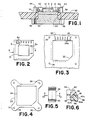
- For a better understanding of the invention, and to show how the same may be carried into effect, reference will now be made, by way of example, to the accompanying drawings in which:
- FIG. 1 is a sectional view of a hybrid circuit mounted to a circuit board,
- FIG. 2 is a top plan view of the hybrid circuit,
- FIG. 3 is a partial top plan view of the circuit board,
- FIG. 4 is a top plan view of a first component shown in FIG. 1,
- FIG. 5 is a partial bottom plan view of a second component shown in FIG. 1, and
- FIG. 6 is a sectional view on the line VI-VI of FIG. 5.
- A hybrid
integrated circuit 2 comprises a monolithic integrated circuit chip that is mounted on asubstrate 6 of ceramic material. The contact pads of the chip are connected to conductor runs 8 of the substrate by bondwires (not shown). Alid 10 is fitted over the chip and is attached to the substrate, leaving the peripheral region of the substrate exposed. The conductor runs 8 extend under the rim of the lid and terminate incontact pads 8a that are exposed in the peripheral region of the substrate. The substrate is generally square in shape, but has one corner cut off at 45 degrees. - A
circuit board 20 is formed with anaperture 22 that extends right through the circuit board and is of the same shape as the substrate. Thus, the aperture is square, except that it has one corner cut off at 45 degrees. The substrate is placed in the aperture of the circuit board, and the shaping of thesubstrate 6 and theaperture 22 ensures that the substrate can be inserted into the aperture in only one position. The circuit board includes conductor runs 24 that terminate about the periphery of the aperture inrespective connection pads 24a. Theconnection pads 8a are distributed about the aperture in a pattern that corresponds to the pattern of terminal areas 6a about the peripheral region of the substrate. The circuit board is formed withholes 26, one adjacent each corner of theaperture 22. Theaperture 22 and theholes 26 are precisely positioned relative to the connection pads 26a. - A metal
heat sink member 30 is in th e form of a generally rectangularplate having ears 32 at its four corners and apedestal 34 at its upper surface. The cross-sectional shape of the pedestal is substantially the same as the shape of the substrate and the aperture, i.e. square with one corner cut off at 45 degrees. Theears 32 are formed with internally threadedholes 36 that are at the same positions relative to the pedestal as theholes 26 in the circuit board are relative to theaperture 22. Thus, when thepedestal 34 is inserted upwardly into theaperture 22, theholes 36 of the heat sink member are aligned with theholes 26 of the circuit board. - A
retaining frame 40 has foursides 42 and is generally square in configuration. At the underside of the frame, the four sides are formed with anendless recess 46. A frame-like body 48 of elastomeric material hasdiscrete strips 50 of metal bonded to its lower face and includes aridge 52 that extends upwardly and fits in therecess 46 of the retaining frame. The retaining frame includes anear 54 at each corner, similar to thehead sink member 30, and each ear is formed with ahole 56. The positioning of theholes 56 relative to each other is the same as that of theholes 26 in the circuit board. Theears 54 extend downwardly beyond thesides 42 of the frame and have abutment surfaces 58. - The
frame 40 is identical to the frame that is used in the practical implementation of the device described in U.S. Patent No. 4,255,003. The innerlower surface portion 60a is at a height of 1.45 mm relative to the abutment surfaces 58 of the ears 54 (which coincide with the top face of the circuit board), whereas the outer lower surface portion 60b is at a height of 0.81 mm. The body of elastomeric material is similar to that which is used in the practical implementation of the device described in U.S. Patent No. 4,255,003, and has inner andouter lobes groove 66 therebetween. However, whereas thelobe 62b extends 1.02 mm below the surface 60b, thelobe 62a extends 1.65 mm below thesurface 60a. The metal strips 50 may be of substantially the same width (0.64 mm) and at substantially the same spacing (0.64 mm) as theconnection pads pads body 48 relative to the circuit board. In this case, thebody 48 may be made using the techniques disclosed in co-pending Application Serial No. filed (Attorney Docket No. USA 4111). -
Screws 64 are fitted through theholes 56 of the retaining frame and theholes 26 of the circuit board and engage theholes 36 of the heat sink member and are used to draw the retaining frame and the heat sink member together. The body of elastomeric material is compressed between the sides of the frame and both the circuit board and the substrate. Engagement of the abutment surfaces 58 of theears 54 of the frame with the upper surface of the circuit board limits the extent to which the elastomeric material is compressed. Thestrips 50 of conductive material contact thecontact pads 8a of the substrate and thecontact pads 24a of the circuit board. Compression of the elastomeric material provides contact force for the pressure contact between the conductive strips and the contact pads, and also maintains the back face of the substrate in contact with the pedestal of the heat sink member. Therefore, electrical connection is provided between eachsubstrate pad 8a and the correspondingcircuit board pad 24a, and a good thermally-conductive contact is provided between the substrate and the heat sink member. - Because the back face of the
substrate 6 is in direct contact with theheat sink member 30, the amount of heat that can be removed from thechip 4 is essentially independent of the thickness and nature of thecircuit board 20. - In an implementation of the in vention, the thickness of the
substrate 6, the thickness of thecircuit board 20 and the height of thepedestal 34 are selected so that the top face of thesubstrate 6 is nominally flush with the top face of thecircuit board 20, and therefore when thescrews 64 are tightened, the inner lobe is compressed to a thickness of 1.45 mm. This degree of compression provides adequate contact force between the metal strips 50 and thecontact pads 8a. The actual position of the top face of the substrate relative to the top face of the circuit board depends on manufacturing tolerances, which are such that the range of probable values for the contact force between the metal strips 50 and the contact pads 6a are acceptable. - It will be appreciated that the present invention is not restricted to the particular embodiment that has been described and illustrated, and that variations may be made therein without departing from the scope of the invention as defined in the appended claims and equivalents thereof.
Claims (5)
Applications Claiming Priority (2)
| Application Number | Priority Date | Filing Date | Title |
|---|---|---|---|
| US06/912,898 US4731693A (en) | 1986-09-29 | 1986-09-29 | Connection apparatus for integrated circuit |
| US912898 | 1986-09-29 |
Publications (2)
| Publication Number | Publication Date |
|---|---|
| EP0262284A1 true EP0262284A1 (en) | 1988-04-06 |
| EP0262284B1 EP0262284B1 (en) | 1991-10-02 |
Family
ID=25432654
Family Applications (1)
| Application Number | Title | Priority Date | Filing Date |
|---|---|---|---|
| EP87101550A Expired EP0262284B1 (en) | 1986-09-29 | 1987-02-05 | Connection apparatus for integrated circuit |
Country Status (4)
| Country | Link |
|---|---|
| US (1) | US4731693A (en) |
| EP (1) | EP0262284B1 (en) |
| JP (1) | JPS6390159A (en) |
| DE (1) | DE3773456D1 (en) |
Families Citing this family (25)
| Publication number | Priority date | Publication date | Assignee | Title |
|---|---|---|---|---|
| US4804172A (en) * | 1987-11-24 | 1989-02-14 | Advanced Micro Devices, Inc. | Fixture for mounting a heat sink |
| US4914812A (en) * | 1987-12-04 | 1990-04-10 | General Electric Company | Method of self-packaging an IC chip |
| DE3837975A1 (en) * | 1988-11-09 | 1990-05-10 | Telefunken Electronic Gmbh | ELECTRONIC CONTROL UNIT |
| GB2236213A (en) * | 1989-09-09 | 1991-03-27 | Ibm | Integral protective enclosure for an assembly mounted on a flexible printed circuit board |
| JPH0726873Y2 (en) * | 1989-10-09 | 1995-06-14 | 三菱電機株式会社 | Electronic component mounting device |
| US5095404A (en) * | 1990-02-26 | 1992-03-10 | Data General Corporation | Arrangement for mounting and cooling high density tab IC chips |
| US4993958A (en) * | 1990-05-23 | 1991-02-19 | Tektronix, Inc. | High density planar interconnect |
| US5287247A (en) * | 1990-09-21 | 1994-02-15 | Lsi Logic Corporation | Computer system module assembly |
| JP2901091B2 (en) * | 1990-09-27 | 1999-06-02 | 株式会社日立製作所 | Semiconductor device |
| US5162975A (en) * | 1991-10-15 | 1992-11-10 | Hewlett-Packard Company | Integrated circuit demountable TAB apparatus |
| US5283467A (en) * | 1992-06-05 | 1994-02-01 | Eaton Corporation | Heat sink mounting system for semiconductor devices |
| US5424918A (en) * | 1994-03-31 | 1995-06-13 | Hewlett-Packard Company | Universal hybrid mounting system |
| US5581443A (en) * | 1994-09-14 | 1996-12-03 | Kabushiki Kaisha Toshiba | Structure for cooling a circuit module having a circuit board and a heat-generating IC chip mounted on the board, and portable electronic apparatus incorporating the structure |
| US5784256A (en) * | 1994-09-14 | 1998-07-21 | Kabushiki Kaisha Toshiba | Portable computer having a circuit board including a heat-generating IC chip and a metal frame supporting the circuit board |
| JP2844558B2 (en) * | 1995-06-29 | 1999-01-06 | 信越ポリマー株式会社 | Wiring circuit board for mounting chip-shaped semiconductor element and method of manufacturing the same |
| US5825625A (en) * | 1996-05-20 | 1998-10-20 | Hewlett-Packard Company | Heat conductive substrate mounted in PC board for transferring heat from IC to heat sink |
| US5960535A (en) * | 1997-10-28 | 1999-10-05 | Hewlett-Packard Company | Heat conductive substrate press-mounted in PC board hole for transferring heat from IC to heat sink |
| US6840777B2 (en) * | 2000-11-30 | 2005-01-11 | Intel Corporation | Solderless electronics packaging |
| US6563696B1 (en) * | 2001-10-17 | 2003-05-13 | Ciena Corporation | Solderless laser assembly |
| US7355854B2 (en) * | 2006-06-07 | 2008-04-08 | Harris Corporation | Apparatus for improved grounding of flange mount field effect transistors to printed wiring boards |
| CN101601131A (en) | 2007-02-15 | 2009-12-09 | 日本电气株式会社 | Structure for mounting semiconductor packages |
| US7638814B2 (en) * | 2007-06-19 | 2009-12-29 | Philips Lumileds Lighting Company, Llc | Solderless integrated package connector and heat sink for LED |
| JP6333215B2 (en) * | 2015-05-19 | 2018-05-30 | オムロンオートモーティブエレクトロニクス株式会社 | Printed circuit boards, electronic devices |
| US10939536B1 (en) * | 2019-09-16 | 2021-03-02 | Ciena Corporation | Secondary side heatsink techniques for optical and electrical modules |
| JP7247915B2 (en) * | 2020-02-14 | 2023-03-29 | 株式会社デンソー | power converter |
Citations (3)
| Publication number | Priority date | Publication date | Assignee | Title |
|---|---|---|---|---|
| FR2156006A1 (en) * | 1971-10-04 | 1973-05-25 | Ibm | |
| US4255003A (en) * | 1975-11-13 | 1981-03-10 | Tektronix, Inc. | Electrical connector |
| FR2574615A1 (en) * | 1984-12-11 | 1986-06-13 | Silicium Semiconducteur Ssc | HOUSING FOR HIGH-FREQUENCY POWER COMPONENT COOLED BY WATER CIRCULATION |
Family Cites Families (2)
| Publication number | Priority date | Publication date | Assignee | Title |
|---|---|---|---|---|
| FR2520932A1 (en) * | 1982-02-02 | 1983-08-05 | Thomson Csf | INTEGRATED CIRCUIT BOX MOUNTING BRACKET, WITH DISTRIBUTED OUTPUT CONNECTIONS ON THE PERIMETER OF THE HOUSING |
| DE3204683A1 (en) * | 1982-02-11 | 1983-08-18 | Brown, Boveri & Cie Ag, 6800 Mannheim | Device for cooling electrical or electronic components which produce lost heat |
-
1986
- 1986-09-29 US US06/912,898 patent/US4731693A/en not_active Expired - Lifetime
-
1987
- 1987-02-05 DE DE8787101550T patent/DE3773456D1/en not_active Expired - Fee Related
- 1987-02-05 EP EP87101550A patent/EP0262284B1/en not_active Expired
- 1987-09-29 JP JP62245700A patent/JPS6390159A/en active Granted
Patent Citations (3)
| Publication number | Priority date | Publication date | Assignee | Title |
|---|---|---|---|---|
| FR2156006A1 (en) * | 1971-10-04 | 1973-05-25 | Ibm | |
| US4255003A (en) * | 1975-11-13 | 1981-03-10 | Tektronix, Inc. | Electrical connector |
| FR2574615A1 (en) * | 1984-12-11 | 1986-06-13 | Silicium Semiconducteur Ssc | HOUSING FOR HIGH-FREQUENCY POWER COMPONENT COOLED BY WATER CIRCULATION |
Non-Patent Citations (1)
| Title |
|---|
| 34TH ELECTRONIC COMPONENTS CONFERENCE, New Orleans, Louisiana, 14th-16th May 1984, pages 138-143, IEEE, New York, US; D.L. TIMMINS: "An elastomeric interconnect system for fine pitch leadless chip carriers" * |
Also Published As
| Publication number | Publication date |
|---|---|
| EP0262284B1 (en) | 1991-10-02 |
| DE3773456D1 (en) | 1991-11-07 |
| JPH0454380B2 (en) | 1992-08-31 |
| JPS6390159A (en) | 1988-04-21 |
| US4731693A (en) | 1988-03-15 |
Similar Documents
| Publication | Publication Date | Title |
|---|---|---|
| EP0262284B1 (en) | Connection apparatus for integrated circuit | |
| US4758927A (en) | Method of mounting a substrate structure to a circuit board | |
| US5109320A (en) | System for connecting integrated circuit dies to a printed wiring board | |
| JPH0713191Y2 (en) | connector | |
| US5421079A (en) | High density, high performance memory circuit package | |
| US5065282A (en) | Interconnection mechanisms for electronic components | |
| US6421244B1 (en) | Power module | |
| JPH0712069B2 (en) | Electronic component package | |
| JPS6333320B2 (en) | ||
| JPH0350844A (en) | Ic chip assembly and connecting and cooling method of the same | |
| CA2327330A1 (en) | Capacitive mounting arrangement for securing an integrated circuit package to a heat sink | |
| JPH09312357A (en) | Semiconductor device | |
| US6989995B2 (en) | Capacitor mounting structure | |
| EP0245179A3 (en) | System for detachably mounting semiconductors on conductor substrate. | |
| US4658330A (en) | Mounting a hybrid circuit to a circuit board | |
| EP0685884A1 (en) | Pressure equalizer for an integrated circuit chip interconnected to circuitry on a thin film membrane | |
| EP0105628B1 (en) | Electrical connector for an electronic package | |
| JP2504486B2 (en) | Hybrid integrated circuit structure | |
| JPS5958855A (en) | Power semiconductor module | |
| JPH0431741Y2 (en) | ||
| JP2936845B2 (en) | Integrated circuit mounting structure | |
| JPH0412676Y2 (en) | ||
| JP2580905Y2 (en) | Semiconductor device | |
| JPH03191554A (en) | Semiconductor device | |
| JP2813683B2 (en) | Substrate for mounting electronic components |
Legal Events
| Date | Code | Title | Description |
|---|---|---|---|
| PUAI | Public reference made under article 153(3) epc to a published international application that has entered the european phase |
Free format text: ORIGINAL CODE: 0009012 |
|
| 17P | Request for examination filed |
Effective date: 19870205 |
|
| AK | Designated contracting states |
Kind code of ref document: A1 Designated state(s): DE FR GB NL |
|
| 17Q | First examination report despatched |
Effective date: 19900131 |
|
| GRAA | (expected) grant |
Free format text: ORIGINAL CODE: 0009210 |
|
| AK | Designated contracting states |
Kind code of ref document: B1 Designated state(s): DE FR GB NL |
|
| REF | Corresponds to: |
Ref document number: 3773456 Country of ref document: DE Date of ref document: 19911107 |
|
| ET | Fr: translation filed | ||
| PLBE | No opposition filed within time limit |
Free format text: ORIGINAL CODE: 0009261 |
|
| STAA | Information on the status of an ep patent application or granted ep patent |
Free format text: STATUS: NO OPPOSITION FILED WITHIN TIME LIMIT |
|
| 26N | No opposition filed | ||
| PGFP | Annual fee paid to national office [announced via postgrant information from national office to epo] |
Ref country code: GB Payment date: 19960119 Year of fee payment: 10 |
|
| PGFP | Annual fee paid to national office [announced via postgrant information from national office to epo] |
Ref country code: NL Payment date: 19960123 Year of fee payment: 10 |
|
| PGFP | Annual fee paid to national office [announced via postgrant information from national office to epo] |
Ref country code: DE Payment date: 19960124 Year of fee payment: 10 |
|
| PGFP | Annual fee paid to national office [announced via postgrant information from national office to epo] |
Ref country code: FR Payment date: 19960201 Year of fee payment: 10 |
|
| PG25 | Lapsed in a contracting state [announced via postgrant information from national office to epo] |
Ref country code: GB Effective date: 19970205 |
|
| PG25 | Lapsed in a contracting state [announced via postgrant information from national office to epo] |
Ref country code: NL Effective date: 19970901 |
|
| GBPC | Gb: european patent ceased through non-payment of renewal fee |
Effective date: 19970205 |
|
| PG25 | Lapsed in a contracting state [announced via postgrant information from national office to epo] |
Ref country code: FR Effective date: 19971030 |
|
| PG25 | Lapsed in a contracting state [announced via postgrant information from national office to epo] |
Ref country code: DE Effective date: 19971101 |
|
| NLV4 | Nl: lapsed or anulled due to non-payment of the annual fee |
Effective date: 19970901 |
|
| REG | Reference to a national code |
Ref country code: FR Ref legal event code: ST |