EP0261620A2 - Circuit arrangement and bus circuit with a large bandwidth, and a component for a broadband switching network - Google Patents
Circuit arrangement and bus circuit with a large bandwidth, and a component for a broadband switching network Download PDFInfo
- Publication number
- EP0261620A2 EP0261620A2 EP87113757A EP87113757A EP0261620A2 EP 0261620 A2 EP0261620 A2 EP 0261620A2 EP 87113757 A EP87113757 A EP 87113757A EP 87113757 A EP87113757 A EP 87113757A EP 0261620 A2 EP0261620 A2 EP 0261620A2
- Authority
- EP
- European Patent Office
- Prior art keywords
- signal
- bandwidth
- circuit arrangement
- circuit
- arrangement according
- Prior art date
- Legal status (The legal status is an assumption and is not a legal conclusion. Google has not performed a legal analysis and makes no representation as to the accuracy of the status listed.)
- Ceased
Links
Images


Classifications
-
- H—ELECTRICITY
- H04—ELECTRIC COMMUNICATION TECHNIQUE
- H04L—TRANSMISSION OF DIGITAL INFORMATION, e.g. TELEGRAPHIC COMMUNICATION
- H04L12/00—Data switching networks
- H04L12/28—Data switching networks characterised by path configuration, e.g. LAN [Local Area Networks] or WAN [Wide Area Networks]
- H04L12/40—Bus networks
- H04L12/4013—Management of data rate on the bus
-
- H—ELECTRICITY
- H04—ELECTRIC COMMUNICATION TECHNIQUE
- H04B—TRANSMISSION
- H04B3/00—Line transmission systems
-
- H—ELECTRICITY
- H04—ELECTRIC COMMUNICATION TECHNIQUE
- H04Q—SELECTING
- H04Q3/00—Selecting arrangements
- H04Q3/42—Circuit arrangements for indirect selecting controlled by common circuits, e.g. register controller, marker
- H04Q3/52—Circuit arrangements for indirect selecting controlled by common circuits, e.g. register controller, marker using static devices in switching stages, e.g. electronic switching arrangements
- H04Q3/521—Circuit arrangements for indirect selecting controlled by common circuits, e.g. register controller, marker using static devices in switching stages, e.g. electronic switching arrangements using semiconductors in the switching stages
Definitions
- the invention relates to a circuit arrangement according to the preamble of claim 1, a bus circuit according to the preamble of claim 7 and a broadband switching matrix device according to the preamble of claim 8.
- a broadband switching matrix module in which a connection between one of several signal inputs and one of several signal outputs can be established by a plurality of coupling points, has such a bus circuit for each signal output, with one driver circuit being available for each signal input and bus circuit.
- the bandwidth of such a broadband switching module depends directly on the number of signal inputs. For a given technology and for a given bandwidth, the size of the switching matrix is also given, provided that no measures can be taken to increase the bandwidth in the given technology.
- the invention is remedied by a circuit arrangement according to the teaching of claim 1, a bus circuit according to the teaching of claim 7 and a broadband switching matrix module according to the teaching of claim 8.
- the fixed potential is advantageously chosen in the middle of the supply voltage, in the case of analog circuits at the operating point. If a second resistor is added, which is connected to a second point with a different potential, there is a voltage divider with which both the effective resistance and a potential that does not influence the function of the circuit can be set. In the case of integrated circuit technology in particular, the resistors are advantageously implemented by transistors.
- the circuit measure according to the invention naturally has not only advantageous effects.
- the signal swing is reduced because the product of gain and bandwidth is constant.
- the use of transistors has the advantage that they can be switched off when this part of the circuit is not required and that the control can be adapted to the bandwidth actually required by changing the control. Because of the reduction in the signal swing and the associated additional interference possibilities, such a measure should only be taken where it is absolutely necessary, ie between those two stages in the course of a signal path between which the bandwidth is most limited.
- a broadband switching matrix module in which a signal between a signal input and a signal output passes through a series of signal conditioning and monitoring circuits, e.g. input and output isolating amplifiers and synchronization circuits, in addition to the actual switching matrix, the greatest band limitation occurs in the switching matrix, as already described the bus circuits that lead to a common signal output.
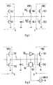
- a transmitting part S is connected to a receiving part E via a signal line L.
- Transmitting part S and receiving part E are any two successive stages in the course of a signal path.
- the transmitting part S is characterized by an internal resistance Ri and an original voltage source uo.
- the original voltage source uo is shown in the drawing as the source of a digital signal.
- the receiving part E is characterized by an input resistance Re. It is assumed that the signal line L is so short that it does not have to be terminated with its characteristic impedance. In such cases, the input resistance Re is orders of magnitude larger than the internal resistance Ri.
- the output of the transmitting part S, the input of the receiving part E and the signal line L have inevitable capacitances, which is shown in FIG. 1 as capacitance C going to ground are drawn. It is evident that the internal resistance Ri and the capacitance C form a low pass.
- the input resistance Re is connected in parallel with the internal resistance Ri in terms of alternating current and does not fundamentally change the low-pass characteristic.
- a further resistance Ra is now connected in parallel with the internal resistance Ri in terms of alternating current. Basically, this does not change the low-pass behavior; however, the upper limit frequency and thus the bandwidth can be increased significantly.
- This basic circuit also shows that the signal swing is reduced by this measure.
- auxiliary voltage source UH is inserted between the resistor Ra and ground in FIG.
- This auxiliary voltage source UH which is a DC voltage source, has no influence on the frequency response of the circuit arrangement.
- Resistor Ra can be connected to any point of fixed potential.
- the ground and supply voltage potentials that are present anyway come into question.
- the fixed potential can also be in the middle of the supply voltage. This is particularly important when the circuit arrangement is non-linear.
- FIG. 2 shows a practical embodiment of the basic circuit of FIG. 1.
- the transmitting part contains a driver circuit consisting of two transistors TS1 and TS2, which is between the supply voltage VDD and ground. Both transistors TS1 and TS2 are driven together, one of the two being conductive and the other blocking.
- the receiving part S contains, likewise between the supply voltage VDD and ground, a similar input circuit consisting of two transistors TE1 and TE2, which are controlled by the output signal of the transmitting part S via the signal line L.
- the resistor Ra is connected to half the supply voltage VDD / 2.
- FIG. 3 shows a slight modification of the example according to FIG. 2.
- the resistor Ra is divided into two resistors R1 and R2, one of which is connected to ground, the other to the supply voltage VDD.
- the auxiliary voltage can thus be influenced via the ratio of the resistors R1 and R2 and the bandwidth can be influenced via the absolute value of the two resistors.
- FIG. 4 shows a modification of the circuit according to FIG. 3 for the practically very significant case in which the circuit arrangement is part of an integrated circuit.
- the resistors R1 and R2 are also designed as transistors, here Ta1 and Ta2.
- the control of the two transistors via a control Voltage Us1 and a control voltage Us2 are DC-voltage, can be both permanently connected and can be set as desired from the outside. This makes it possible to keep the reduction in the signal swing and the power loss in the transistors Ta1 and Ta2 as small as possible, depending on the respective application.
- FIG. 5 shows a further exemplary embodiment which combines features of the exemplary embodiment according to FIG. 2 and features of the exemplary embodiment according to FIG. 4.
- the resistor Ra in FIG. 2 is replaced here by a parallel connection of two transistors Ta1 and Ta2. These are driven in opposite directions by means of a control voltage Us with the aid of an inverter (not specified in more detail), so that they are both switched on or both switched off because of the opposite polarity.
- This circuit arrangement can only be used for a switchover that is sufficient for many practical cases.
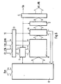
- FIG. 6 shows the block diagram of a broadband switching matrix module with 16 signal inputs E1 to E16, 16 extension inputs EX1 to EX16, a clock input TE, a clock output TA, 16 signal outputs A1 to A16 and a control data bus BUS.
- the signal paths reach the inside of the broadband switching matrix module via input isolating amplifier 3 and back out again via output isolating amplifier 4.
- the signals arriving via the signal inputs E1 to E16 are synchronized in an input synchronization device 1, and before leaving the broadband switching matrix module they are synchronized again in an output synchronization device 2.
- the expansion inputs EX1 to EX16 are connected to signal outputs A1 to A16 of a spatially immediately adjacent preceding switching matrix.
- the core of the broadband switching matrix is a switching matrix K.
- a monitoring device 5 is arranged at the output of the switching matrix K, which allows the 16 output signals to be monitored.
- a decoding and control device 6 is provided for controlling the coupling matrix K and for monitoring using the monitoring device 5. Further details on this switching matrix module, which, however, are not necessary for an understanding of the present invention, are contained in the following German patent applications: P 34 41 501.7, P 35 04 835.2, P 35 10 566.6 and P 35 43 392.2.
- the coupling matrix K is made up of rows and columns, each row being assigned to one of the signal outputs A1 to A16 and each column to one of the signal inputs E1 to E16 or one of the extension inputs EX1 to EX16.
- a coupling point K0101 to K1616 is arranged at the intersection of a column, which is assigned to one of the signal inputs E1 to E16, with a row.
- Each coupling point has two pairs of transistors, one pair of transistors being driven by a control signal St and the second pair of transistors by the signal coming from the assigned signal input.
- the control signal is inverted at each crosspoint, so that either both transistors of the associated transistor pair are open or both are closed.
- the control signal St comes from the decoding and control device 6.
- Each coupling point forms a driver circuit, at most one driver circuit is active, while all others are blocked and represent a capacitive load for the active driver circuit.
- a large number of further signal inputs can be indirectly connected to this bus circuit via the associated extension input, which can be connected to the associated signal output of a preceding broadband switching matrix device, without significantly burdening it.
- This is one way of increasing the number of signal inputs for a given bandwidth.
- the invention now provides a further possibility for increasing the number of signal inputs for a given bandwidth. This is equivalent to the possibility of increasing the bandwidth for a given number of signal inputs.
- an additional resistor is inserted. This is represented in FIG. 7 by the circuits designated as resistors R1 to R16.
- the control signals St can be used primarily to make this circuit high-impedance when the outputs are not connected. *
Landscapes
- Engineering & Computer Science (AREA)
- Computer Networks & Wireless Communication (AREA)
- Signal Processing (AREA)
- Quality & Reliability (AREA)
- Electronic Switches (AREA)
- Logic Circuits (AREA)
- Dc Digital Transmission (AREA)
- Cable Transmission Systems, Equalization Of Radio And Reduction Of Echo (AREA)
- Use Of Switch Circuits For Exchanges And Methods Of Control Of Multiplex Exchanges (AREA)
Abstract
Description
Die Erfindung betrifft eine Schaltungsanordnung nach dem Oberbegriff des Anspruchs 1, eine Busschaltung nach dem Oberbegriff des Anspruchs 7 und einen Breitbandkoppelfeldbaustein nach dem Oberbegriff des Anspruchs 8.The invention relates to a circuit arrangement according to the preamble of
Nahezu jede elektrische Schaltungsanordnung fällt unter den Oberbegriff des Anspruchs 1. Ausgenommen hiervon sind vor allem Filter, bei denen die Bandbreite durch gezielte Maßnahmen begrenzt ist. Grundsätzlich jedoch ist bei jeder elektrischen Schaltungsanordnung die Bandbreite durch die obere Grenzfrequenz begrenzt. Das Problem der begrenzten Bandbreite ist von so grundsätzlicher Bedeutung, daß auch schon sehr viele fertige Lösungen vorliegen. Beispielsweise gibt es auf dem Gebiet der digitalen Logikschaltungen mehrere Schaltungsfamilien, die hinsichtlich ihrer logischen Funktionen gleich sind, jedoch unter anderem was die Bandbreite betrifft, unterschiedlich sind. In Grenzbereichen spielt dieses Problem aber immer eine große Rolle. So kann beispielsweise in einer integrierten Schaltung der Längswiderstand einer Leitung, also auch eines Kanals in einem Transistor, durch Vergrößerung des Leitungsquerschnitts verringert werden. Die Kapazität wird dabei aber im selben Maß erhöht, so daß das Produkt aus Widerstand und Kapazität gleich bleibt. Da aber ein Leitungslängswiderstand zusammen mit einer Querkapazität einen Tiefpaß bildet, dessen Grenzfrequenz vom Produkt aus Widerstand und Kapazität abhängt, kann durch derartige geometrische Maßnahmen die Bandbreite nicht erhöht werden. Dieses Problem verschärft sich bei einer Busschaltung, wo eine Mehrzahl von Treiberschaltungen auf eine gemeinsame Signalleitung geschaltet sind. Dabei müssen immer alle Treiberschaltungen bis auf eine gesperrt sein, um einen ordnungsgemäßen Betrieb zu gewährleisten. Die Kapazitäten der gesperrten Treiberschaltungen bilden dann eine zusätzliche Last für die nicht gesperrte Treiberschaltung. Dagegen sind die Kapazitäten der Signalleitung selbst und daran angeschlossener Signaleingänge von untergeordneter Bedeutung. Ein Breitbandkoppelfeldbaustein, bei dem durch eine Vielzahl von Koppelpunkten je eine Verbindung zwischen einem von mehreren Signaleingängen und einem von mehreren Signalausgängen herstellbar ist, weist pro Signalausgang eine solche Busschaltung auf, wobei pro Signaleingang und Busschaltung eine Treiberschaltung vorhanden ist. Die Bandbreite eines solchen Breitbandkoppelfeldbausteins hängt damit direkt von der Zahl der Signaleingänge ab. Bei gegebener Technologie und bei vorgegebener Bandbreite ist damit auch die Größe des Koppelfelds vorgegeben, sofern keine in der vorgegebenen Technologie realisierbaren Maßnahmen zur Erhöhung der Bandbreite ergriffen werden können.Almost every electrical circuit arrangement falls under the preamble of
Bei diesen Problemen schafft die Erfindung Abhilfe durch eine Schaltungsanordnung nach der Lehre des Anspruchs 1, eine Busschaltung nach der Lehre des Anspruchs 7 und einen Breitbandkoppelfeldbaustein nach der Lehre des Anspruchs 8.In the case of these problems, the invention is remedied by a circuit arrangement according to the teaching of
Durch Einfügen eines Widerstands zwischen die Signalleitung und einen Punkt mit festem Potential wird wechselstrommäßig dem Innenwiderstand ein Widerstand parallel geschaltet, so daß sich der für den Tiefpaß wirksame Widerstand effektiv verringert, wodurch die Bandbreite erhöht wird. Um Nichtlinearitäten zu berücksichtigen wird das feste Potential vorteilhaft in der Mitte der Versorgungsspannung, bei Analogschaltungen im Arbeitspunkt, gewählt. Fügt man einen zweiten Widerstand hinzu, der mit einem zweiten Punkt mit abweichendem Potential verbunden ist, so liegt ein Spannungsteiler vor, mit dem sowohl der effektive Widerstand als auch ein die Funktion der Schaltung möglichst nicht beeinflussendes Potential einstellbar ist. Insbesondere bei integrierter Schaltungstechnik werden die Widerstände in vorteilhafter Weise durch Transistoren realisiert. Die erfindungsgemäße Schaltungsmaßnahme hat natürlich nicht nur vorteilhafte Wirkungen. Zum einen ergibt sich ein zusätzlicher Leistungsverbrauch, zum anderen wird der Signalhub verringert, da das Produkt aus Verstärkung und Bandbreite konstant ist. Die Verwendung von Transistoren hat den Vorteil, daß sie abgeschaltet werden können, wenn dieser Teil der Schaltung nicht benötigt wird und daß durch Änderung der Ansteuerung eine Anpassung an die tatsächlich benötigte Bandbreite möglich ist. Wegen der Reduzierung des Signalhubs und der damit verbundenen zusätzlichen Störmöglichkeiten sollte eine solche Maßnahme aber nur dort erfolgen, wo es unbedingt nötig ist, d.h. zwischen denjenigen beiden Stufen im Verlauf eines Signalwegs, zwischen denen die Bandbreite am meisten begrenzt ist. Bei einem Breitbandkoppelfeldbaustein, bei dem ein Signal zwischen einem Signaleingang und einem Signalausgang außer dem eigentlichen Koppelfeld noch eine Reihe von Signalaufbereitungs- und Überwachungsschaltungen, z.B. Eingangs- und Ausgangstrennverstärker und -synchronisierschaltungen, durchläuft, tritt die größte Bandbegrenzung, wie schon beschrieben, im Koppelfeld in den Busschaltungen auf, die zu einem gemeinsamen Signalausgang führen.By inserting a resistor between the signal line and a fixed potential point AC resistance in parallel with the internal resistance, so that the effective for the low-pass resistance is effectively reduced, whereby the bandwidth is increased. In order to take nonlinearities into account, the fixed potential is advantageously chosen in the middle of the supply voltage, in the case of analog circuits at the operating point. If a second resistor is added, which is connected to a second point with a different potential, there is a voltage divider with which both the effective resistance and a potential that does not influence the function of the circuit can be set. In the case of integrated circuit technology in particular, the resistors are advantageously implemented by transistors. The circuit measure according to the invention naturally has not only advantageous effects. On the one hand there is an additional power consumption, on the other hand the signal swing is reduced because the product of gain and bandwidth is constant. The use of transistors has the advantage that they can be switched off when this part of the circuit is not required and that the control can be adapted to the bandwidth actually required by changing the control. Because of the reduction in the signal swing and the associated additional interference possibilities, such a measure should only be taken where it is absolutely necessary, ie between those two stages in the course of a signal path between which the bandwidth is most limited. In the case of a broadband switching matrix module in which a signal between a signal input and a signal output passes through a series of signal conditioning and monitoring circuits, e.g. input and output isolating amplifiers and synchronization circuits, in addition to the actual switching matrix, the greatest band limitation occurs in the switching matrix, as already described the bus circuits that lead to a common signal output.
Im folgenden wird die Erfindung anhand von Ausführungsbeispielen unter Zuhilfenahme der beiliegenden Zeichnung weiter erläutert.
Figur 1 zeigt ein Ersatzschaltbild zur Erklärung der Wirkungsweise einer erfindungsgemäßen Schaltungsanordnung.Figuren 2 bis 5 zeigen Ausführungsbeispiele erfindungsgemäßer Schaltungsanordnungen.Figur 6 zeigt das Blockschaltbild eines erfindungsgemäß ausgebildeten Breitbandkoppelfeldbausteins.- Figur 7 zeigt das Koppelfeld des Breitbandkoppelfeldbausteins gemäß
Figur 6. Es weist eine Mehrzahl erfindungsgemäßer Busschaltungen auf.
- FIG. 1 shows an equivalent circuit diagram to explain the mode of operation of a circuit arrangement according to the invention.
- Figures 2 to 5 show exemplary embodiments of circuit arrangements according to the invention.
- FIG. 6 shows the block diagram of a broadband switching matrix module designed according to the invention.
- FIG. 7 shows the switching matrix of the broadband switching matrix module according to FIG. 6. It has a plurality of bus circuits according to the invention.
Zunächst wird anhand der Figur 1 der Grundgedanke der Erfindung erläutert. Ein Sendeteil S ist über eine Signalleitung L mit einem Empfangsteil E verbunden. Sendeteil S und Empfangsteil E sind zwei beliebige aufeinanderfolgende Stufen im Verlauf eines Signalwegs. Das Sendeteil S ist charakterisiert durch einen Innenwiderstand Ri und eine Urspannungsquelle uo. Die Urspannungsquelle uo ist in der Zeichnung als Quelle eines Digitalsignals dargestellt. Das Empfangsteil E ist charakterisiert durch einen Eingangswiderstand Re. Es wird davon ausgegangen, daß die Signalleitung L so kurz ist, daß sie nicht mit ihrem Wellenwiderstand abgeschlossen werden muß. In solchen Fällen ist der Eingangswiderstand Re um Größenordnungen größer als der Innenwiderstand Ri. Der Ausgang des Sendeteils S, der Eingang des Empfangsteils E und die Signalleitung L sind mit unvermeidlichen Kapazitäten behaftet, die in Figur 1 als nach Masse gehende Kapazität C einge zeichnet sind. Es ist offensichtlich, daß der Innenwiderstand Ri und die Kapazität C einen Tiefpaß bilden. Der Eingangswiderstand Re ist wechselstrommäßig dem Innenwiderstand Ri parallel geschaltet und ändert grundsätzlich nichts an der Tiefpaßeigenschaft.First, the basic idea of the invention is explained with reference to FIG. 1. A transmitting part S is connected to a receiving part E via a signal line L. Transmitting part S and receiving part E are any two successive stages in the course of a signal path. The transmitting part S is characterized by an internal resistance Ri and an original voltage source uo. The original voltage source uo is shown in the drawing as the source of a digital signal. The receiving part E is characterized by an input resistance Re. It is assumed that the signal line L is so short that it does not have to be terminated with its characteristic impedance. In such cases, the input resistance Re is orders of magnitude larger than the internal resistance Ri. The output of the transmitting part S, the input of the receiving part E and the signal line L have inevitable capacitances, which is shown in FIG. 1 as capacitance C going to ground are drawn. It is evident that the internal resistance Ri and the capacitance C form a low pass. The input resistance Re is connected in parallel with the internal resistance Ri in terms of alternating current and does not fundamentally change the low-pass characteristic.
Erfindungsgemäß ist nun ein weiterer Widerstand Ra wechselstrommäßig dem Innenwiderstand Ri parallel geschaltet. Grundsätzlich ändert sich dadurch das Tiefpaßverhalten nicht; die obere Grenzfrequenz und damit die Bandbreite können dadurch jedoch deutlich erhöht werden. An dieser Prinzipschaltung ist aber auch schon erkennbar, daß der Signalhub durch diese Maßnahme reduziert wird. Der Innenwiderstand Ri und der Widerstand Ra bilden, zusammen mit dem praktisch vernachlässigbar hohen Eingangswiderstand Re einen Spannungsteiler. Ein nicht unerheblicher Teil der Signalamplitude liegt hierbei bereits am Innenwiderstand Ri und wirkt sich am Empfangsteil E nicht mehr aus. Hier ist erkennbar, daß diese Maßnahme ein Notbehelf ist und nicht bedenkenlos angewendet werden sollte.According to the invention, a further resistance Ra is now connected in parallel with the internal resistance Ri in terms of alternating current. Basically, this does not change the low-pass behavior; however, the upper limit frequency and thus the bandwidth can be increased significantly. This basic circuit also shows that the signal swing is reduced by this measure. The internal resistance Ri and the resistance Ra, together with the practically negligible high input resistance Re, form a voltage divider. A not inconsiderable part of the signal amplitude is already due to the internal resistance Ri and no longer has an effect on the receiving part E. It can be seen here that this measure is a makeshift measure and should not be used without hesitation.
Des weiteren ist in Figur 1 noch eine Hilfsspannungsquelle UH zwischen den Widerstand Ra und Masse eingefügt. Diese Hilfsspannungsquelle UH, die eine Gleichspannungsquelle ist, hat auf den Frequenzgang der Schaltungsanordnung keinen Einfluß. Der Widerstand Ra kann mit jedem Punkt festen Potentials verbunden sein. Insbesondere kommen die ohnehin vorhandenen Masse- und Versorgungsspannungspotentiale in Frage. Um die Gleichspannungsverhältnisse nicht zu beeinflussen oder einen Arbeitspunkt einzustellen, kann das feste Potential auch in der Mitte der Versorgungsspannung liegen. Dies ist vor allem dann von Bedeutung, wenn die Schaltungsanordnung nichtlinear ist.Furthermore, an auxiliary voltage source UH is inserted between the resistor Ra and ground in FIG. This auxiliary voltage source UH, which is a DC voltage source, has no influence on the frequency response of the circuit arrangement. Resistor Ra can be connected to any point of fixed potential. In particular, the ground and supply voltage potentials that are present anyway come into question. In order not to influence the DC voltage conditions or to set an operating point, the fixed potential can also be in the middle of the supply voltage. This is particularly important when the circuit arrangement is non-linear.
Figur 2 zeigt eine praktische Ausgestaltung der Prinzipschaltung von Figur 1. Das Sendeteil enthält eine aus zwei Transistoren TS1 und TS2 bestehende Treiberschaltung, die zwischen der Versorgungsspannung VDD und Masse liegt. Beide Transistoren TS1 und TS2 werden gemeinsam angesteuert, wobei jeweils einer der beiden leitend, der andere sperrend ist. Das Empfangsteil S enthält, ebenfalls zwischen der Versorgungsspannung VDD und Masse, eine gleichartige, aus zwei Transistoren TE1 und TE2 bestehende Eingangsschaltung, die über die Signalleitung L vom Ausgangssignal des Sendeteils S angesteuert werden. Der Widerstand Ra ist in diesem Beispiel mit der halben Versorgungsspannung VDD/2 verbunden.FIG. 2 shows a practical embodiment of the basic circuit of FIG. 1. The transmitting part contains a driver circuit consisting of two transistors TS1 and TS2, which is between the supply voltage VDD and ground. Both transistors TS1 and TS2 are driven together, one of the two being conductive and the other blocking. The receiving part S contains, likewise between the supply voltage VDD and ground, a similar input circuit consisting of two transistors TE1 and TE2, which are controlled by the output signal of the transmitting part S via the signal line L. In this example, the resistor Ra is connected to half the supply voltage VDD / 2.
Wie diese halbe Versorgungsspannung VDD/2 erzeugt wird, ist in diesem Beispiel nicht gezeigt. Eine für mehrere gleichartige Schaltungsanordnungen gemeinsam erzeugte Hilfsspannung von der Größe VDD/2 ist wegen der dann erforderlichen Leitungsführung und einer möglichen Signalverkopplung über den Innenwiderstand der Hilfsspannungsquelle manchmal unerwünscht.How this half supply voltage VDD / 2 is generated is not shown in this example. An auxiliary voltage of VDD / 2 size generated jointly for a plurality of similar circuit arrangements is sometimes undesirable because of the then required line routing and a possible signal coupling via the internal resistance of the auxiliary voltage source.
Figur 3 zeigt eine geringfügige Abwandlung des Beispiels nach Figur 2. Der Widerstand Ra ist aufgeteilt in zwei Widerstände R1 und R2, von denen der eine mit Masse, der andere mit der Versorgungsspannung VDD verbunden ist. Damit kann über das Verhältnis der Widerstände R1 und R2 die Hilfsspannung und über den Absolutwert der beiden Widerstände die Bandbreite beeinflußt werden.FIG. 3 shows a slight modification of the example according to FIG. 2. The resistor Ra is divided into two resistors R1 and R2, one of which is connected to ground, the other to the supply voltage VDD. The auxiliary voltage can thus be influenced via the ratio of the resistors R1 and R2 and the bandwidth can be influenced via the absolute value of the two resistors.
Figur 4 zeigt eine Abwandlung der Schaltung nach Figur 3 für den praktisch sehr bedeutsamen Fall, daß die Schaltungsanordnung Bestandteil einer integrierten Schaltung ist. In diesem Fall werden auch die Widerstände R1 und R2 als Transistoren, hier Ta1 und Ta2 ausgeführt. Die Ansteuerung der beiden Transistoren über eine Steuer spannung Us1 und eine Steuerspannung Us2 erfolgt gleichspannungsmäßig, kann sowohl fest verschaltet, als auch von außen beliebig einstellbar sein. Damit ist es möglich, die Reduzierung des Signalhubs und die Verlustleistung in den Transistoren Ta1 und Ta2 in Abhängigkeit vom jeweiligen Einsatzfall so gering wie möglich zu halten.FIG. 4 shows a modification of the circuit according to FIG. 3 for the practically very significant case in which the circuit arrangement is part of an integrated circuit. In this case, the resistors R1 and R2 are also designed as transistors, here Ta1 and Ta2. The control of the two transistors via a control Voltage Us1 and a control voltage Us2 are DC-voltage, can be both permanently connected and can be set as desired from the outside. This makes it possible to keep the reduction in the signal swing and the power loss in the transistors Ta1 and Ta2 as small as possible, depending on the respective application.
Figur 5 zeigt ein weiteres Ausführungsbeispiel, das Merkmale des Ausführungsbeispiels nach Figur 2 und Merkmale des Ausführungsbeispiels nach Figur 4 in sich vereinigt. Der Widerstand Ra von Figur 2 ist hier durch eine Parallelschaltung zweier Transistoren Ta1 und Ta2 ersetzt. Diese werden durch eine Steuerspannung Us unter Zuhilfenahme eines nicht näher bezeichneten Inverters gegensinnig angesteuert, so daß sie, der gegensinnigen Polarität wegen, jeweils beide ein- oder beide ausgeschaltet sind. Mit dieser Schaltungsanordnung kann nur eine Umschaltung erfolgen, die für viele praktische Fälle ausreicht.FIG. 5 shows a further exemplary embodiment which combines features of the exemplary embodiment according to FIG. 2 and features of the exemplary embodiment according to FIG. 4. The resistor Ra in FIG. 2 is replaced here by a parallel connection of two transistors Ta1 and Ta2. These are driven in opposite directions by means of a control voltage Us with the aid of an inverter (not specified in more detail), so that they are both switched on or both switched off because of the opposite polarity. This circuit arrangement can only be used for a switchover that is sufficient for many practical cases.
Figur 6 zeigt das Blockschaltbild eines Breitbandkoppelfeldbausteins mit 16 Signaleingängen E1 bis E16, 16 Erweiterungseingängen EX1 bis EX16,einem Takteingang TE, einem Taktausgang TA, 16 Signalausgängen A1 bis A16 und einem Steuerdatenbus BUS. Die Signalwege gelangen über Eingangstrennverstärker 3 ins Innere des Breitbandkoppelfeldbausteins und über Ausgangstrennverstärker 4 wieder nach außen. Die über die Signaleingänge E1 bis E16 ankommenden Signale werden in einer Eingangssynchronisationseinrichtung 1 synchronisiert,vor Verlassen des Breitbandkoppelfeldbausteins werden sie in einer Ausgangssynchronisationseinrichtung 2 erneut synchronisiert. Die Erweiterungseingänge EX1 bis EX16 sind mit Signalausgängen A1 bis A16 eines räumlich unmittelbar benachbarten vorangehenden Koppelfeldbausteins verbunden. Ihre Signale brauchen deshalb nicht synchronisisert werden. Kern des Breitbandkoppelfelds ist eine Koppelmatrix K. Am Ausgang der Koppelmatrix K ist eine Überwachungseinrichtung 5 angeordnet, die es erlaubt, die 16 Ausgangssignale zu überwachen. Zur Ansteuerung der Koppelmatrix K und zur Überwachung mit Hilfe der Überwachungseinrichtung 5 ist eine Decodier- und Steuereinrichtung 6 vorhanden. Nähere Einzelheiten zu diesem Koppelfeldbaustein, die aber für das Verständnis der vorliegenden Erfindung nicht erforderlich sind, sind in den folgenden Deutschen Patentanmeldungen enthalten: P 34 41 501.7, P 35 04 835.2, P 35 10 566.6 und P 35 43 392.2.FIG. 6 shows the block diagram of a broadband switching matrix module with 16 signal inputs E1 to E16, 16 extension inputs EX1 to EX16, a clock input TE, a clock output TA, 16 signal outputs A1 to A16 and a control data bus BUS. The signal paths reach the inside of the broadband switching matrix module via input isolating amplifier 3 and back out again via
Die Koppelmatrix K und ihre erfindungsgemäße Ausgestaltung wird nun anhand der Figur 7 näher erläutert.The coupling matrix K and its configuration according to the invention will now be explained in more detail with reference to FIG. 7.
Die Koppelmatrix K ist aus Zeilen und Spalten aufgebaut, wobei jede Zeile einem der Signalausgänge A1 bis A16 und jede Spalte einem der Signaleingänge E1 bis E16 oder einem der Erweiterungseingänge EX1 bis EX16 zugeordnet ist. Am Schnittpunkt einer Spalte, die einem der Signaleingänge E1 bis E16 zugeordnet ist,mit einer Zeile ist jeweils ein Koppelpunkt K0101 bis K1616 angeordnet. Jeder Koppelpunkt weist zwei Transistorpaare auf, wobei ein Transistorpaar durch ein Steuersignal St und das zweite Transistorpaar durch das vom zugeordneten Signaleingang kommende Signal angesteuert wird. Das Steuersignal wird in jedem Koppelpunkt noch invertiert, so daß entweder beide Transistoren des zugehörigen Transistorpaars geöffnet oder beide geschlossen sind. Das Steuersignal St kommt von der Decodier- und Steuereinrichtung 6. Damit wird festgelegt, welches der Eingangssignale zu einem bestimmten Signalausgang durchgeschaltet wird. Das zweite Transistorpaar wird gleichsinnig angesteuert, so daß wegen der gegensinnigen Polarität der Transistoren immer einer der beiden geöffnet und der andere geschlossen ist. Gleichartige Koppelpunkte KX1 bis KX16 sind auch dort, wo sich eine von den Erweiterungseingänge EX1 bis EX16 kommende Spalte mit der zum zugehörigen Signalausgang gehenden Zeile kreuzt. Es kann also vom Erweiterungseingang EX1 zum Signalausgang A1, vom Erweiterungseingang EX2 zum Signalausgang A2 usw. durchgeschaltet werden. Jede zu einem Signalausgang führende Zeile bildet also eine aus einer Anzahl von Koppelpunkten, einer Signalleitung L1 bis L16 und dem Eingang der nachfolgenden Baugruppe*bestehende Busschaltung. Jeder Koppelpunkt bildet eine Treiberschaltung, wobei höchstens eine Treiberschaltung aktiv ist, während alle anderen gesperrt sind und eine kapazitive Last für die aktive Treiberschaltung darstellen. Über den zugehörigen Erweiterungseingang, der mit dem zugehörigen Signalausgang eines vorangehenden Breitbandkoppelfeldbausteins verbunden sein kann, kann eine Vielzahl weiterer Signaleingänge indirekt mit dieser Busschaltung verbunden sein, ohne sie nennenswert zu belasten. Dies stellt eine Möglichkeit dar, um bei vorgegebener Bandbreite die Zahl der Signaleingänge erhöhen zu können. Die Erfindung gibt nun eine weitere Möglichkeit an, um bei gegebener Bandbreite die Zahl der Signaleingänge erhöhen zu können. Dies ist gleichwertig mit der Möglichkeit,bei gegebener Zahl der Signaleingänge die Bandbreite zu erhöhen. Hierzu wird, wie in den vorangegangenen Ausführungsbeispielen gezeigt, ein zusätzlicher Widerstand eingefügt. Dies ist in Figur 7 durch die als Widerstände R1 bis R16 bezeichneten Schaltungen dargestellt. Die Steuersignale St können hierbei in erster Linie dazu verwendet werden, bei nicht beschalteten Ausgängen diese Schaltung hochohmig zu machen.
* Hier Überwachungseinrichtung 5The coupling matrix K is made up of rows and columns, each row being assigned to one of the signal outputs A1 to A16 and each column to one of the signal inputs E1 to E16 or one of the extension inputs EX1 to EX16. At the intersection of a column, which is assigned to one of the signal inputs E1 to E16, with a row, a coupling point K0101 to K1616 is arranged. Each coupling point has two pairs of transistors, one pair of transistors being driven by a control signal St and the second pair of transistors by the signal coming from the assigned signal input. The control signal is inverted at each crosspoint, so that either both transistors of the associated transistor pair are open or both are closed. The control signal St comes from the decoding and
* Here monitoring device 5
Claims (8)
Applications Claiming Priority (2)
| Application Number | Priority Date | Filing Date | Title |
|---|---|---|---|
| DE19863632218 DE3632218A1 (en) | 1986-09-23 | 1986-09-23 | CIRCUIT ARRANGEMENT AND BUS CIRCUIT WITH HIGH BANDWIDTH AND BROADBAND COUPLING FIELD BLOCK |
| DE3632218 | 1986-09-23 |
Publications (2)
| Publication Number | Publication Date |
|---|---|
| EP0261620A2 true EP0261620A2 (en) | 1988-03-30 |
| EP0261620A3 EP0261620A3 (en) | 1988-10-05 |
Family
ID=6310106
Family Applications (1)
| Application Number | Title | Priority Date | Filing Date |
|---|---|---|---|
| EP87113757A Ceased EP0261620A3 (en) | 1986-09-23 | 1987-09-21 | Circuit arrangement and bus circuit with a large bandwidth, and a component for a broadband switching network |
Country Status (4)
| Country | Link |
|---|---|
| EP (1) | EP0261620A3 (en) |
| JP (1) | JPS6387018A (en) |
| AU (1) | AU593382B2 (en) |
| DE (1) | DE3632218A1 (en) |
Cited By (1)
| Publication number | Priority date | Publication date | Assignee | Title |
|---|---|---|---|---|
| EP0339719A1 (en) * | 1988-04-25 | 1989-11-02 | AT&T NETWORK SYSTEMS INTERNATIONAL B.V. | Switching matrix for telecommunication exchanges |
Citations (3)
| Publication number | Priority date | Publication date | Assignee | Title |
|---|---|---|---|---|
| JPS59108430A (en) * | 1982-12-13 | 1984-06-22 | Matsushita Electric Ind Co Ltd | Binary-ternary value converting circuit |
| JPS60224356A (en) * | 1984-04-23 | 1985-11-08 | Nec Corp | Bus circuit |
| US4585958A (en) * | 1983-12-30 | 1986-04-29 | At&T Bell Laboratories | IC chip with noise suppression circuit |
Family Cites Families (1)
| Publication number | Priority date | Publication date | Assignee | Title |
|---|---|---|---|---|
| JPS5362479A (en) * | 1976-11-16 | 1978-06-03 | Nec Corp | Integrated circuit with power terminals for testing |
-
1986
- 1986-09-23 DE DE19863632218 patent/DE3632218A1/en not_active Withdrawn
-
1987
- 1987-09-10 AU AU78255/87A patent/AU593382B2/en not_active Ceased
- 1987-09-21 EP EP87113757A patent/EP0261620A3/en not_active Ceased
- 1987-09-22 JP JP62236386A patent/JPS6387018A/en active Pending
Patent Citations (3)
| Publication number | Priority date | Publication date | Assignee | Title |
|---|---|---|---|---|
| JPS59108430A (en) * | 1982-12-13 | 1984-06-22 | Matsushita Electric Ind Co Ltd | Binary-ternary value converting circuit |
| US4585958A (en) * | 1983-12-30 | 1986-04-29 | At&T Bell Laboratories | IC chip with noise suppression circuit |
| JPS60224356A (en) * | 1984-04-23 | 1985-11-08 | Nec Corp | Bus circuit |
Non-Patent Citations (3)
| Title |
|---|
| PATENT ABSTRACTS OF JAPAN, Band 10, Nr. 79 (E-391)[2136], 28. März 1986; & JP-A-60 224 356 (NIPPON DENKI K.K.) 08-11-1985 * |
| PATENT ABSTRACTS OF JAPAN, Band 8, Nr. 229 (E-273)[1666], 20. Oktober 1984; & JP-A-59 108 430 (MATSUSHITA DENKI SANGYO K.K.) 22-06-1984 * |
| PROCEEDINGS OF THE INTERNATIONAL SWITCHING SYMPOSIUM, TELECOMMUNICATION SWITCHING, Florenz, 7.-11. Mai 1984, Teil 2, "Session 31C, paper 3", Seiten 1-6, North Holland Publ. Co., Amsterdam NL; C. DURET et al.: "Integrated crosspoint technology for wide band space division switching networks" * |
Cited By (1)
| Publication number | Priority date | Publication date | Assignee | Title |
|---|---|---|---|---|
| EP0339719A1 (en) * | 1988-04-25 | 1989-11-02 | AT&T NETWORK SYSTEMS INTERNATIONAL B.V. | Switching matrix for telecommunication exchanges |
Also Published As
| Publication number | Publication date |
|---|---|
| AU7825587A (en) | 1988-03-31 |
| DE3632218A1 (en) | 1988-03-31 |
| JPS6387018A (en) | 1988-04-18 |
| AU593382B2 (en) | 1990-02-08 |
| EP0261620A3 (en) | 1988-10-05 |
Similar Documents
| Publication | Publication Date | Title |
|---|---|---|
| DE3215671C2 (en) | Programmable logic arrangement | |
| EP0096944A1 (en) | Circuit with several signal paths formed by active arrangements | |
| EP0591561B1 (en) | Integrated circuit for generating a reset signal | |
| DE2036306A1 (en) | Multiple amplifiers, especially in an integrated circuit, with step decoupling | |
| DE2643020A1 (en) | SCHMITT TRIGGER | |
| DE1813580C3 (en) | Circuit arrangement for an electronic coordinate coupler in telecommunications, in particular telephone switching systems | |
| DE2932587C2 (en) | Broadband switching arrangement with a matrix of switching point circuits in ECL technology | |
| DE102004055939B4 (en) | switching matrix | |
| EP0148395B1 (en) | Matrix broad-band coupling field | |
| DE3327488C2 (en) | Bidirectional amplifier for bidirectional data lines | |
| DE4420988A1 (en) | Method for testing an integrated circuit and integrated circuit arrangement with a test circuit | |
| EP0262480B1 (en) | Current mirror circuit arrangement | |
| DE1268669B (en) | Multi-stable circuit | |
| DE2251444C2 (en) | Coupling matrix arrangement for broadband signal transmission in telecommunications systems | |
| DE2208829A1 (en) | ||
| DE1922382C3 (en) | Electronic switching matrix device with field effect transistors | |
| EP0142182B1 (en) | Circuit arrangement for the conversion of a digital input signal to an analogous output signal | |
| EP0261620A2 (en) | Circuit arrangement and bus circuit with a large bandwidth, and a component for a broadband switching network | |
| EP0057239A1 (en) | Monolithic integrated push-pull driver circuit | |
| EP0588111B1 (en) | Memory element | |
| DE2002578C3 (en) | Multi-stable circuit | |
| EP1198880B1 (en) | Arrangement comprising a first and a second amplifier whereby a maximum of one of said amplifiers amplifies | |
| DE4421419A1 (en) | MOS driver circuit | |
| DE3032970C2 (en) | Circuit arrangement for symmetrizing the operating points of electronically DC-fed connecting lines in telecommunications systems, in particular telephone exchanges | |
| DE19959426C1 (en) | Signal coupling element for coupling field |
Legal Events
| Date | Code | Title | Description |
|---|---|---|---|
| PUAI | Public reference made under article 153(3) epc to a published international application that has entered the european phase |
Free format text: ORIGINAL CODE: 0009012 |
|
| AK | Designated contracting states |
Kind code of ref document: A2 Designated state(s): AT BE CH DE ES FR GB IT LI NL SE |
|
| RAP3 | Party data changed (applicant data changed or rights of an application transferred) |
Owner name: ALCATEL N.V. Owner name: STANDARD ELEKTRIK LORENZ AKTIENGESELLSCHAFT |
|
| PUAL | Search report despatched |
Free format text: ORIGINAL CODE: 0009013 |
|
| AK | Designated contracting states |
Kind code of ref document: A3 Designated state(s): AT BE CH DE ES FR GB IT LI NL SE |
|
| 17P | Request for examination filed |
Effective date: 19890218 |
|
| 17Q | First examination report despatched |
Effective date: 19890609 |
|
| STAA | Information on the status of an ep patent application or granted ep patent |
Free format text: STATUS: THE APPLICATION HAS BEEN REFUSED |
|
| 18R | Application refused |
Effective date: 19900414 |
|
| RIN1 | Information on inventor provided before grant (corrected) |
Inventor name: PREISACH, HELMUT Inventor name: KLEIN, MICHAEL, DR. Inventor name: WOELK, JOACHIM Inventor name: BANNIZA, THOMAS |