EP0261352B1 - Cross point switch architecture for a micro-pbx - Google Patents
Cross point switch architecture for a micro-pbx Download PDFInfo
- Publication number
- EP0261352B1 EP0261352B1 EP87111111A EP87111111A EP0261352B1 EP 0261352 B1 EP0261352 B1 EP 0261352B1 EP 87111111 A EP87111111 A EP 87111111A EP 87111111 A EP87111111 A EP 87111111A EP 0261352 B1 EP0261352 B1 EP 0261352B1
- Authority
- EP
- European Patent Office
- Prior art keywords
- line
- receive
- switch
- transmit
- cross point
- Prior art date
- Legal status (The legal status is an assumption and is not a legal conclusion. Google has not performed a legal analysis and makes no representation as to the accuracy of the status listed.)
- Expired
Links
- 238000004891 communication Methods 0.000 claims description 8
- 238000010586 diagram Methods 0.000 description 13
- 230000009977 dual effect Effects 0.000 description 9
- 230000006870 function Effects 0.000 description 6
- 238000012544 monitoring process Methods 0.000 description 6
- 101710092886 Integrator complex subunit 3 Proteins 0.000 description 2
- 102100025254 Neurogenic locus notch homolog protein 4 Human genes 0.000 description 2
- 230000001143 conditioned effect Effects 0.000 description 2
- 238000005516 engineering process Methods 0.000 description 2
- 239000011159 matrix material Substances 0.000 description 2
- 230000004044 response Effects 0.000 description 2
- 102100024061 Integrator complex subunit 1 Human genes 0.000 description 1
- 101710092857 Integrator complex subunit 1 Proteins 0.000 description 1
- 101710092887 Integrator complex subunit 4 Proteins 0.000 description 1
- 102100037075 Proto-oncogene Wnt-3 Human genes 0.000 description 1
- 230000002457 bidirectional effect Effects 0.000 description 1
- 230000005540 biological transmission Effects 0.000 description 1
- 230000001702 transmitter Effects 0.000 description 1
Images


Classifications
-
- H—ELECTRICITY
- H04—ELECTRIC COMMUNICATION TECHNIQUE
- H04M—TELEPHONIC COMMUNICATION
- H04M3/00—Automatic or semi-automatic exchanges
- H04M3/42—Systems providing special services or facilities to subscribers
- H04M3/56—Arrangements for connecting several subscribers to a common circuit, i.e. affording conference facilities
-
- H—ELECTRICITY
- H04—ELECTRIC COMMUNICATION TECHNIQUE
- H04Q—SELECTING
- H04Q3/00—Selecting arrangements
- H04Q3/42—Circuit arrangements for indirect selecting controlled by common circuits, e.g. register controller, marker
- H04Q3/52—Circuit arrangements for indirect selecting controlled by common circuits, e.g. register controller, marker using static devices in switching stages, e.g. electronic switching arrangements
Definitions
- the invention disclosed broadly relates to data processor control of telephone switching and more particularly relates to telephone communication path switching in a personal computer system.
- dual tone multifrequency trans mitters and receivers enable the user to transmit call establishment signals over the network.
- Other devices such as automatic dialers and answer tone detectors enable the automatic establishment of calls between unattended stations.
- it is inefficient to simultaneously gang switch both the transmit and the receive paths for a particular telephonic session, and indeed such simultaneous gang switching as is practiced by the prior art limits the flexibility in the connectivity of a modern telephone system.
- PBX dial private branch exchange
- the invention is a software reconfigurable cross point switch which selectively interconnects a plurality of phone lines and a plurality of shared resources such as call progress monitors, dual tone multifrequency (DTMF) receivers, DTMF automatic dialers and automatic answer tone detectors.
- the invention achieves its objective of enhanced switching efficiency and greater flexibility in the connectivity between dverse communications elements, by independently switching two separate switching planes of the cross point switch so as to enable different paths to be taken by the transmit portion and the receive portion of a particular telephone connection.
- the cross point switch architecture invention flexibly allows for many applications, one in particular being conference summing. By providing a plurality of build-out resistors connected to the separate inputs of one plane of the cross point switch, and connecting the corresponding outputs from the cross point switch to a single input of the summing amplifier, a conference summing function can be performed.
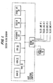
- the host Personal Computer is depicted as including the random access memory (RAM) 20, the read only memory (ROM) 22, the central processing unit (CPU) 24, the keyboard 26, the display 28, and other input/output (I/O) devices 30, interconnected by the address and data bus 32.
- RAM random access memory
- ROM read only memory
- CPU central processing unit
- I/O input/output
- the micro-PBX 34 connected to the bus 32, which is the feature of particular interest herein.
- the micro-PBX 34 functions to inter connect the local phone 49 to the public telephone (Telco) lines #1, #2, #3 and #4, under control of the stored program instructions contained in the RAM 20 of the host Personal Computer.
- the micro-PBX 34 can be embodied as an I/O adapter card which will plug into the I/O adapter bus of the IBM Personal Computer, and will operate by issuing interrupts to the CPU 24, in the manner described in the copending U. S. patent application serial number 770,541, filed August 29, 1985 by David J. Bradley, et al. entitled "System for Managing a Plurality of Shared Interrupt Handlers in a Linked-List Data Structure," assigned to the IBM Corporation and incorporated herein by reference.
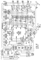
- the micro-PBX 34 is shown in greater detail in the block diagram of Fig. 2 wherein the data bus and address bus 32 is shown connected through the bidirectional bus driver to the adapter data bus.
- the adapter data bus in Fig. 2 provides inputs to the dual tone multifrequency (DTMF) receiver 40, the call progress processor 42, the DTMF/pulse dialer 50, the control latch, the real time clock/calendar, the second control latch and the parallel I/O port, and further to the control block 96.
- the control block 96 includes the operation control, the interrupt handler and the input port and output port, which are described in greater detail in the above referenced, copending patent application to David J. Bradley, et al.
- the control block 96 further includes a timing generator, a channel A universal asynchronous receiver transmitter (UART) and the channel B UART.
- the UARTs are conyentional universal asynchronous receiver transmitters which provide an interface between a digital source of information and a modulator/demo dulator such as is shown between the channel B UART and the frequency shift key (FSK) modem 44.
- the address bus 32 also provides an input to the address decoder of Fig. 2 which provides control outputs DO through D9 and 102 to various elements shown in Fig. 2.
- the Telco lines #1, #2, #3 and #4 are shown connected to the phone line interfaces (PLI) such as the PLI 100 and the local DT-MF phone 49 is shown with its receiver 46 and transmitter 48 connected through the relay 90 to the two-wire to four-wire converter (2W/4W converter) 98.
- PLI phone line interfaces
- the coil 92 is not energized and therefore the relay 90 and the relay 94 are positioned so that the telephone 49 is directly connected to the Telco line 1.
- the coil 92 is then energized and the Telco line 1 is connected to its respective phone line interface (PLI) and the DTMF telephone 49 is connected to the converter 98.
- interrupt signals INT1 through INT4 are generated in the micro-PBX 34 of Fig. 2.
- the INT3 is generated by the DTMF receiver 40 when the receiver 40 receives a dual - tone multifrequency signal from a telephone line.
- the DTMF receiver 40 outputs the INT3 interrupt signal to the input port of the control block 96 which, in response thereto, has the interrupt handler output an IRQ2 signal on the interrupt bus to the CPU 24, in accordance with the David J. Bradley, et al. copending patent application, cited above.
- a conference summing amplifier 52 is shown in Fig.
- a dual plane cross point switch is provided in the form of a receive switch 36 constituting the first plane and the transmit switch 38 constituting the second plane.
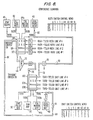
- the receive switch 36 is shown in greater detail in Fig. 3 and the transmit switch 38 is shown in greater detail in Fig. 4.
- the receive switch 36 consists of an array of transfer gates 00 through Q15 whose respective conduction paths, which can conduct a signal in either direction, are controlled by the address A1 through A4 applied to the four line-to-16 line decoder 33 whose output is connected to the 16 control latch block 35.
- the four-bit binary address A1 through A4 is applied to the decoder 33, it is translated into one of 16 energized signals on the lines connected to the latch block 35, when an RX select signal is applied to the decoder 33 and the strobe signal is present on the decoder 33.
- the corresponding energized one of the 16 latches in the latch block 35 then is set to either a zero or a one state in accordance with the zero or one binary value applied to the data terminal of the latch.
- a binary value of one is applied to the data terminal, then the particular one of the connected cross point switch elements 00 through Q15 being address, is turned on and becomes conductive, otherwise if the data is zero, the element is turned off.
- the fifth line of 16 lines output from the decoder 33 would be enabled as an input to the latch block 35.
- the fifth latch of the 16 latches in the latch block 35 would then be conditioned to be set to the state of the data input to the latch block 35. If the data value is a binary one, then the fifth latch in the latch block 35 will be turned on.
- the transmit switch 30 of Fig. 4 operates in a similar manner, and accepts the same four bits of binary address A1 through A4, but is selected by the TX select line.
- the corresponding latch in the control latch block 39 is conditioned to be set to the state of the input data to the block 39, thereby appropriately setting the cross point switch element Q'0 through Q'15, in a manner similar to that described for the receive latch 36.
- the receive switch 36 has as its inputs the Telco receive line #4 on RX1A, the Telco receive line #3 on RX2A, the Telco receive line #2 on RX3A, and the Telco receive line #1 on RX4A.
- the receive switch 34 has the DTMF receiver 40 connected to the RX1 B line, the call progress processor 42 connected to the RX2B line, the FSK modem receiver 44A connected to the RX3B line, and the local phone receiver 46 connected to the RX4B line.
- the transmit switch 38 has as its inputs the DTMF/pulse dialer 50 connected to the TX1A line, the sum amplifier 52 connected to the TX2A line, the FSK modem transmitter 44B connected to the TX3A line, and the local phone transmitter 48 connected to the TX4A line. Still further, the transmit switch 38 has the Telco transmit line #4
- the CPU 2 4 will execute a sequence of stored program instructions in the RAM 20, to carry out various call processing interconnection functions by applying a sequence of receive switch control words to the decoder 33 in the receive switch 36 and the sequence of transmit switch control words to the decoder 37 in the transmit switch 38.
- This will selectively interconnect a plurality of telephone lines such as the Telco lines 1, 2, 3 and 4 with the DTMF receiver 40, the call progress processor 42, the FSK modem 44, the local phone 49, the DTMF/pulse dialer 50, the sum amplifier 52, and other shared resource elements, in order to achieve functions such as call progress tone monitoring, answer tone monitoring, call forwarding between a first line and a second line, call conferencing with up to five users, DTMF tone monitoring (including the recordation and display of the last number dialed), data modem switching onto any line, selective line hold function, selective private conversation in a multi-user conversation mode, and other multiple line/multiple resource applications. Examples of some of these applications are depicted in Figs. 5 through 8.
- Fig. 5 depicts the micro-PBX 34 in a schematic diagram, performing manual dialing with the storage of the last number dialed.
- the CPU 24 applies a sequence of three receive switch control words to switch the state of elements QO, Q12 and Q15 of the receive switch 36, as shown in Fig. 5.
- the CPU 24 further applies a transmit switch control word to set the state of the element Q' 15 in the transmit switch 38, as shown in Fig. 5.
- the tone signals are output on line 60 and are applied through the conductive switch element Q' 15 of the transmit switch 38 to the Telco transmit line #1.
- the DTMF tones on line 60 are also applied over line 62 through the gate 54 and over the line 64 to the RX1A line of the receive switch 36.
- Line 64 is connected through the conductive element QO to the RX1B line, applying the tone signals to the DTMF receiver 40.
- the DT-MF receiver 40 will convert the tone signals into digital values which are passed back to the CPU 24 and stored as the last number dialed. Later, this number can be called up and automatically applied to dial the last number, as desired.
- Line 64 being connected through the element QO in the receive switch 36, passes over line 66 to the conductive element Q12 where it continues to propagate over the line 68 to the conductive element Q15.
- Conductive element Q15 passes the signal from line 68 to line 70 and then out onto the RX4B line to the local phone receiver 46, so as to enable the local user to listen to his DTMF tones as dialed.
- An important advantage accruing from the invention is that a different pattern of receive switch control words is applied to the receive switch 36 than the pattern of transmit switch control words applied to the transmit switch 38. This is an illustration of the flexible connectivity of the dual plane cross point switch architecture, in accordance with the invention.
- Fig. 6 is a schematic diagram of the micro-PBX 34, carrying out an auto dialing and call progress monitoring function.
- the CPU 24 under control of the stored program instructions in the RAM 20, will apply the receive switch control word for the element Q5 shown in Fig. 6 and the transmit switch control word for the element Q'4 shown in Fig. 6. This will connect the RX2A line for the Telco receive line #3 through the element Q5 of the receive switch 36, to the line RX2B connected to the call progress processor 42 of Fig. 6.
- the transmit switch 38 will have the DTMF/pulse dialer 50 connected by means of line TX1A, through the element Q'4 of the transmit switch 38, to the line TX2B for the Telco transmit line #3.
- Fig. 7 is a schematic diagram of the micro-PBX 34 illustrating an example stage which might occur after that depicted in Fig. 6, where the FSK modem will enter into transmit and receive operations, after the successful completion of the placement of the call carried out by the operation of Fig. 6.
- the receive switch control word for Q6 and a transmit switch control word for Q'6 are supplied by the CPU 24 under the control of the stored program instructions in the RAM 20. This will set the Q6 element in the receive switch 36 so as to connect the RX2A line for the Telco receive line #3, to the FSK modem receiver 44A over the RX3B line.
- the transmit switch control word will cause the Q' 6 element to connect the FSK modem transmitter 44B over the line TX3A, to the Telco transmit line #3 over the line TX2B.
- Fig. 8 shows an improved conference summing configuration used in conjunction with the dual plane cross point switch architecture.
- Fig. 8 shows the build-out resistors R1, R2, R3 and R4 which are connected between the receive switch 36 lines RXIA, RX2A, RX3A and RX4A and the corresponding Telco receive lines #4, #3, #2 and #1, respectively.
- RX1 B line of the receive switch 36 Also connected to the RX1 B line of the receive switch 36 is the negative terminal of the summing amplifier 72, the positive terminal of which is connected to ground potential.
- the output of summing amplifier 72 is connected through resistor R6 to line 74 which connects to the TX1A line of the transmit switch 38. Also shown in Fig.
- the CPU 24 under control of the stored program instructions in the RAM 20, provides the receive switch control words for Q0, Q8 and Q12 as shown in Fig.
- the output of the amplifier 72 which passes through the resistor R6 and over the line 74 to the transmit switch 38, allows the analog sum of the signals to be distributed to the local telephone receiver 46 by means of the line 76, and to the Telco transmit line #2 over line TX3B and to the Telco transmit line #1 over the line TX4B from the transmit switch 38.
- the summing amplifier 72 can include a feedback resistor from its output to the input line thereof in classic summing amplifier configuration.
- the resistance of the transfer gate devices Q0, Q8 and Q12 in the receive switch 36 is between 200 and 400 ohms.
- the build-out resistors R3, R4 and R5 are designed to have a resistance of approximately 22,000 ohms. In this manner, if one or more cross point switch elements Q0, Q8 or Q12 are connected serially through a particular analog connection from line 64 to the summing amplifier 72, for example, the relative attenuation of the signal will be minimal.
- the single output from the summing amplifier 72 is connected through the resistor R6 which has a resistance of approximately 5,000 ohms, over line 72 to the single input port at transmit switch 38.
- the resultant dual plane cross point switching architecture enables a full range of interconnectivity between shared resource elements such as DTMF tone monitoring and generation units, voice storage and playback units, modems, and the Telco communication lines or local telephone handsets.
Landscapes
- Engineering & Computer Science (AREA)
- Computer Networks & Wireless Communication (AREA)
- Multimedia (AREA)
- Signal Processing (AREA)
- Telephonic Communication Services (AREA)
- Sub-Exchange Stations And Push- Button Telephones (AREA)
- Exchange Systems With Centralized Control (AREA)
Applications Claiming Priority (2)
| Application Number | Priority Date | Filing Date | Title |
|---|---|---|---|
| US910055 | 1986-09-22 | ||
| US06/910,055 US4803720A (en) | 1986-09-22 | 1986-09-22 | Dual plane cross point switch architecture for a micro-PBX |
Publications (3)
| Publication Number | Publication Date |
|---|---|
| EP0261352A2 EP0261352A2 (en) | 1988-03-30 |
| EP0261352A3 EP0261352A3 (en) | 1988-10-19 |
| EP0261352B1 true EP0261352B1 (en) | 1990-04-25 |
Family
ID=25428243
Family Applications (1)
| Application Number | Title | Priority Date | Filing Date |
|---|---|---|---|
| EP87111111A Expired EP0261352B1 (en) | 1986-09-22 | 1987-07-31 | Cross point switch architecture for a micro-pbx |
Country Status (4)
| Country | Link |
|---|---|
| US (1) | US4803720A (ref) |
| EP (1) | EP0261352B1 (ref) |
| JP (1) | JPS6384294A (ref) |
| DE (1) | DE3762476D1 (ref) |
Families Citing this family (17)
| Publication number | Priority date | Publication date | Assignee | Title |
|---|---|---|---|---|
| US4945534A (en) * | 1987-09-10 | 1990-07-31 | Compunetics, Inc. | Programmable conferencing module for ring arrays and switchable ring array networks |
| USD311401S (en) | 1989-08-25 | 1990-10-16 | Harry Catey | Extension attachment for a telephone earpiece |
| US5182554A (en) * | 1990-12-18 | 1993-01-26 | International Business Machines Corporation | Third party evavesdropping for bus control |
| US5347564A (en) * | 1991-12-20 | 1994-09-13 | The Chesapeake And Potomac Telephone Company Of Maryland | Automated translation input system |
| US5625775A (en) * | 1994-06-13 | 1997-04-29 | International Business Machines Corporation | Modem communication interface in a data processing system |
| US6014431A (en) * | 1996-03-29 | 2000-01-11 | Cisco Technology, Inc. | Communication server apparatus having four-wire switching interface and method |
| US5668857A (en) * | 1996-03-29 | 1997-09-16 | Netspeed, Inc. | Communication server apparatus and method |
| US5781617A (en) | 1996-03-29 | 1998-07-14 | Netspeed, Inc. | Communication server apparatus using frequency multiplexing and method |
| US6151325A (en) * | 1997-03-31 | 2000-11-21 | Cisco Technology, Inc. | Method and apparatus for high-capacity circuit switching with an ATM second stage switch |
| WO1999005590A2 (en) * | 1997-07-25 | 1999-02-04 | Starvox, Inc. | Apparatus and method for integrated voice gateway |
| EP0898409A3 (en) * | 1997-08-19 | 2004-01-07 | Nortel Networks Limited | Communication system architecture, exchange and method of operation |
| US5999565A (en) | 1997-10-15 | 1999-12-07 | Cisco Technology, Inc. | Data communication using a modifiable number of XDSL modems |
| US6522668B1 (en) | 1998-11-30 | 2003-02-18 | Cisco Technology, Inc. | System and method for special signaling with customer premises equipment |
| US8510596B1 (en) * | 2006-02-09 | 2013-08-13 | Virsec Systems, Inc. | System and methods for run time detection and correction of memory corruption |
| JP2016534479A (ja) | 2013-09-12 | 2016-11-04 | ヴァーセック・システムズ・インコーポレーテッドVirsec Systems,Inc. | マルウェアのランタイム中の自動検出 |
| CA2953793C (en) | 2014-06-24 | 2021-10-19 | Virsec Systems, Inc. | System and methods for automated detection of input and output validation and resource management vulnerability |
| CA3027728C (en) | 2016-06-16 | 2026-05-05 | Virsec Systems, Inc. | Systems and methods for remediating memory corruption in a computer application |
Family Cites Families (22)
| Publication number | Priority date | Publication date | Assignee | Title |
|---|---|---|---|---|
| US3546394A (en) * | 1967-12-05 | 1970-12-08 | Itt | Electronic switching telephone system using mos devices |
| US3531773A (en) * | 1968-02-26 | 1970-09-29 | Electronic Communications | Three stage switching matrix |
| US3544726A (en) * | 1968-02-26 | 1970-12-01 | American Telephone & Telegraph | Conference switching system |
| US3577125A (en) * | 1968-10-16 | 1971-05-04 | Itt | Monolithic electronic switching network having variable voltage levels |
| US3588827A (en) * | 1968-11-29 | 1971-06-28 | Philips Corp | Variable linear matrix |
| US3828314A (en) * | 1971-02-03 | 1974-08-06 | Wescom | End mark controlled switching system and matrix |
| US3792200A (en) * | 1971-06-15 | 1974-02-12 | Stromberg Carlson Corp | Matrix switching network control link interconnection circuit |
| DE2216262B2 (de) * | 1972-04-05 | 1975-02-06 | Ibm Deutschland Gmbh, 7000 Stuttgart | Fernsprech-Koppeleinrichtung |
| US3792202A (en) * | 1972-04-26 | 1974-02-12 | Stromberg Carlson Corp | Dial up conference circuit |
| US3814862A (en) * | 1972-11-02 | 1974-06-04 | Gte Automatic Electric Lab Inc | Matrix-protecting supervisory arrangement for a communication switching system |
| GB1411189A (en) * | 1972-12-18 | 1975-10-22 | Arizona Chem | Molecular sieve catalyzed isomerization of terpenes |
| US3903373A (en) * | 1973-04-17 | 1975-09-02 | Stromberg Carlson Corp | Combined operator controlled dial-up conference for PBX |
| US3865979A (en) * | 1973-06-21 | 1975-02-11 | Alfred Hestad | Matrix control circuit |
| US3891801A (en) * | 1974-01-21 | 1975-06-24 | Quindar Electronics | Four-way four-wire active bridge |
| US4046966A (en) * | 1974-04-15 | 1977-09-06 | Tokyo Shibaura Electric Co., Ltd. | Conference trunk circuit for an exchange |
| NL7408823A (ref) * | 1974-07-01 | 1974-09-25 | ||
| US4008376A (en) * | 1975-10-17 | 1977-02-15 | Bell Telephone Laboratories, Incorporated | Loudspeaking teleconferencing circuit |
| US4075608A (en) * | 1976-01-19 | 1978-02-21 | The United States Of America As Represented By The Secretary Of The Navy | Multiple-channel data switch |
| GB1602474A (en) * | 1977-10-06 | 1981-11-11 | Warman B J | Device for establishing conference calls via at least one telephone exchange switching system |
| US4153817A (en) * | 1977-11-25 | 1979-05-08 | Stromberg-Carlson Corporation | Digital conference circuit |
| US4424418A (en) * | 1981-05-18 | 1984-01-03 | Bell Telephone Laboratories, Incorporated | Communication system parkhold conferencing |
| US4605928A (en) * | 1983-10-24 | 1986-08-12 | International Business Machines Corporation | Fault-tolerant array of cross-point switching matrices |
-
1986
- 1986-09-22 US US06/910,055 patent/US4803720A/en not_active Expired - Fee Related
-
1987
- 1987-07-31 DE DE8787111111T patent/DE3762476D1/de not_active Expired - Lifetime
- 1987-07-31 EP EP87111111A patent/EP0261352B1/en not_active Expired
- 1987-08-21 JP JP62206646A patent/JPS6384294A/ja active Granted
Also Published As
| Publication number | Publication date |
|---|---|
| JPH0445038B2 (ref) | 1992-07-23 |
| JPS6384294A (ja) | 1988-04-14 |
| EP0261352A2 (en) | 1988-03-30 |
| EP0261352A3 (en) | 1988-10-19 |
| US4803720A (en) | 1989-02-07 |
| DE3762476D1 (de) | 1990-05-31 |
Similar Documents
| Publication | Publication Date | Title |
|---|---|---|
| US4803720A (en) | Dual plane cross point switch architecture for a micro-PBX | |
| KR930011032B1 (ko) | 호 처리 장치 | |
| CA1205169A (en) | Pulse code modulated digital automatic exchange | |
| US4293946A (en) | Trilateral duplex path conferencing system with broadcast capability | |
| GB2219714A (en) | Telephone systems | |
| US3504130A (en) | Switching system for establishing conference connections | |
| US4538033A (en) | Data bridge with gating and/or testing | |
| US4660219A (en) | Extension ringing arrangement key telephone system | |
| US3306983A (en) | Call transfer system | |
| US3511931A (en) | Conferencing networks employing virtual ground summation to obtain isolation | |
| RU2067356C1 (ru) | Учрежденческая автоматическая телефонная станция с импульсно-временным разделением каналов | |
| GB1570086A (en) | Circuit arrangements for use in telephones exchange systems | |
| RU2040861C1 (ru) | Автоматический телефонный концентратор | |
| JPS58114655A (ja) | 呼出中リセツトシフトコ−ル | |
| JPS63153993A (ja) | ボタン電話装置 | |
| JPS62128260A (ja) | 内線接続機能付網制御装置 | |
| JPS62123891A (ja) | ボタン電話装置間接続方式 | |
| JPH0662453A (ja) | 構内交換電話装置 | |
| JPH01149667A (ja) | プログラマブルマルチポートモデム | |
| JPS585635B2 (ja) | 時分割交換機における同報通信方式 | |
| JPS594372A (ja) | 網制御装置 | |
| JPH01198198A (ja) | アナログ加入者線切替装置 | |
| JPH044788B2 (ref) | ||
| JPS5937754A (ja) | オ−バ−フロ−制御付き同報呼装置 | |
| JPS6286998A (ja) | マルチパ−テイ回線における複数通話システム |
Legal Events
| Date | Code | Title | Description |
|---|---|---|---|
| PUAI | Public reference made under article 153(3) epc to a published international application that has entered the european phase |
Free format text: ORIGINAL CODE: 0009012 |
|
| AK | Designated contracting states |
Kind code of ref document: A2 Designated state(s): DE FR GB |
|
| PUAL | Search report despatched |
Free format text: ORIGINAL CODE: 0009013 |
|
| 17P | Request for examination filed |
Effective date: 19880729 |
|
| AK | Designated contracting states |
Kind code of ref document: A3 Designated state(s): DE FR GB |
|
| 17Q | First examination report despatched |
Effective date: 19890216 |
|
| GRAA | (expected) grant |
Free format text: ORIGINAL CODE: 0009210 |
|
| AK | Designated contracting states |
Kind code of ref document: B1 Designated state(s): DE FR GB |
|
| REF | Corresponds to: |
Ref document number: 3762476 Country of ref document: DE Date of ref document: 19900531 |
|
| ET | Fr: translation filed | ||
| R20 | Corrections of a patent specification |
Effective date: 19900605 |
|
| PLBE | No opposition filed within time limit |
Free format text: ORIGINAL CODE: 0009261 |
|
| STAA | Information on the status of an ep patent application or granted ep patent |
Free format text: STATUS: NO OPPOSITION FILED WITHIN TIME LIMIT |
|
| 26N | No opposition filed | ||
| PGFP | Annual fee paid to national office [announced via postgrant information from national office to epo] |
Ref country code: GB Payment date: 19950622 Year of fee payment: 9 |
|
| PGFP | Annual fee paid to national office [announced via postgrant information from national office to epo] |
Ref country code: FR Payment date: 19950704 Year of fee payment: 9 |
|
| PGFP | Annual fee paid to national office [announced via postgrant information from national office to epo] |
Ref country code: DE Payment date: 19950720 Year of fee payment: 9 |
|
| PG25 | Lapsed in a contracting state [announced via postgrant information from national office to epo] |
Ref country code: GB Effective date: 19960731 |
|
| GBPC | Gb: european patent ceased through non-payment of renewal fee |
Effective date: 19960731 |
|
| PG25 | Lapsed in a contracting state [announced via postgrant information from national office to epo] |
Ref country code: FR Effective date: 19970328 |
|
| PG25 | Lapsed in a contracting state [announced via postgrant information from national office to epo] |
Ref country code: DE Effective date: 19970402 |
|
| REG | Reference to a national code |
Ref country code: FR Ref legal event code: ST |