EP0254823B1 - Lichtelektrische Positionsmesseinrichtung - Google Patents
Lichtelektrische Positionsmesseinrichtung Download PDFInfo
- Publication number
- EP0254823B1 EP0254823B1 EP87106621A EP87106621A EP0254823B1 EP 0254823 B1 EP0254823 B1 EP 0254823B1 EP 87106621 A EP87106621 A EP 87106621A EP 87106621 A EP87106621 A EP 87106621A EP 0254823 B1 EP0254823 B1 EP 0254823B1
- Authority
- EP
- European Patent Office
- Prior art keywords
- measuring device
- coupler
- tbj
- lwl
- position measuring
- Prior art date
- Legal status (The legal status is an assumption and is not a legal conclusion. Google has not performed a legal analysis and makes no representation as to the accuracy of the status listed.)
- Expired - Lifetime
Links
- 230000003287 optical effect Effects 0.000 claims abstract description 15
- 230000005855 radiation Effects 0.000 claims abstract description 7
- 230000002452 interceptive effect Effects 0.000 claims abstract 2
- 239000000758 substrate Substances 0.000 claims description 6
- 239000000835 fiber Substances 0.000 claims description 3
- 230000008878 coupling Effects 0.000 description 9
- 238000010168 coupling process Methods 0.000 description 9
- 238000005859 coupling reaction Methods 0.000 description 9
- 239000004065 semiconductor Substances 0.000 description 5
- 239000013307 optical fiber Substances 0.000 description 3
- 238000006073 displacement reaction Methods 0.000 description 2
- 230000007613 environmental effect Effects 0.000 description 2
- 238000000034 method Methods 0.000 description 2
- 238000010276 construction Methods 0.000 description 1
- 238000013461 design Methods 0.000 description 1
- 238000000609 electron-beam lithography Methods 0.000 description 1
- 238000011156 evaluation Methods 0.000 description 1
- 239000011521 glass Substances 0.000 description 1
- 230000036039 immunity Effects 0.000 description 1
- 238000004519 manufacturing process Methods 0.000 description 1
- 238000005259 measurement Methods 0.000 description 1
- 239000002184 metal Substances 0.000 description 1
- 238000000206 photolithography Methods 0.000 description 1
- 238000012545 processing Methods 0.000 description 1
Images

Classifications
-
- G—PHYSICS
- G02—OPTICS
- G02B—OPTICAL ELEMENTS, SYSTEMS OR APPARATUS
- G02B6/00—Light guides; Structural details of arrangements comprising light guides and other optical elements, e.g. couplings
- G02B6/10—Light guides; Structural details of arrangements comprising light guides and other optical elements, e.g. couplings of the optical waveguide type
- G02B6/12—Light guides; Structural details of arrangements comprising light guides and other optical elements, e.g. couplings of the optical waveguide type of the integrated circuit kind
- G02B6/122—Basic optical elements, e.g. light-guiding paths
- G02B6/124—Geodesic lenses or integrated gratings
-
- G—PHYSICS
- G01—MEASURING; TESTING
- G01D—MEASURING NOT SPECIALLY ADAPTED FOR A SPECIFIC VARIABLE; ARRANGEMENTS FOR MEASURING TWO OR MORE VARIABLES NOT COVERED IN A SINGLE OTHER SUBCLASS; TARIFF METERING APPARATUS; MEASURING OR TESTING NOT OTHERWISE PROVIDED FOR
- G01D5/00—Mechanical means for transferring the output of a sensing member; Means for converting the output of a sensing member to another variable where the form or nature of the sensing member does not constrain the means for converting; Transducers not specially adapted for a specific variable
- G01D5/26—Mechanical means for transferring the output of a sensing member; Means for converting the output of a sensing member to another variable where the form or nature of the sensing member does not constrain the means for converting; Transducers not specially adapted for a specific variable characterised by optical transfer means, i.e. using infrared, visible, or ultraviolet light
- G01D5/32—Mechanical means for transferring the output of a sensing member; Means for converting the output of a sensing member to another variable where the form or nature of the sensing member does not constrain the means for converting; Transducers not specially adapted for a specific variable characterised by optical transfer means, i.e. using infrared, visible, or ultraviolet light with attenuation or whole or partial obturation of beams of light
- G01D5/34—Mechanical means for transferring the output of a sensing member; Means for converting the output of a sensing member to another variable where the form or nature of the sensing member does not constrain the means for converting; Transducers not specially adapted for a specific variable characterised by optical transfer means, i.e. using infrared, visible, or ultraviolet light with attenuation or whole or partial obturation of beams of light the beams of light being detected by photocells
- G01D5/36—Forming the light into pulses
- G01D5/38—Forming the light into pulses by diffraction gratings
-
- H—ELECTRICITY
- H01—ELECTRIC ELEMENTS
- H01M—PROCESSES OR MEANS, e.g. BATTERIES, FOR THE DIRECT CONVERSION OF CHEMICAL ENERGY INTO ELECTRICAL ENERGY
- H01M50/00—Constructional details or processes of manufacture of the non-active parts of electrochemical cells other than fuel cells, e.g. hybrid cells
- H01M50/50—Current conducting connections for cells or batteries
- H01M50/572—Means for preventing undesired use or discharge
- H01M50/574—Devices or arrangements for the interruption of current
- H01M50/581—Devices or arrangements for the interruption of current in response to temperature
-
- Y—GENERAL TAGGING OF NEW TECHNOLOGICAL DEVELOPMENTS; GENERAL TAGGING OF CROSS-SECTIONAL TECHNOLOGIES SPANNING OVER SEVERAL SECTIONS OF THE IPC; TECHNICAL SUBJECTS COVERED BY FORMER USPC CROSS-REFERENCE ART COLLECTIONS [XRACs] AND DIGESTS
- Y02—TECHNOLOGIES OR APPLICATIONS FOR MITIGATION OR ADAPTATION AGAINST CLIMATE CHANGE
- Y02E—REDUCTION OF GREENHOUSE GAS [GHG] EMISSIONS, RELATED TO ENERGY GENERATION, TRANSMISSION OR DISTRIBUTION
- Y02E60/00—Enabling technologies; Technologies with a potential or indirect contribution to GHG emissions mitigation
- Y02E60/10—Energy storage using batteries
Definitions
- the invention relates to a photoelectric position measuring device according to the preamble of claim 1.
- a diffraction grating is the reference measure.
- a diffraction grating consists of very thin grating lines which are formed close together, for example on a glass or metal plate, by mechanical processing, by an optical lithography process or by electron beam lithography.
- a light source which emits monochromatic light, for example laser light
- two reflector mirrors and a detector which is located on the side of the diffraction grating opposite the light source and which receives interference light.
- the light beam emitted by the light source is diffracted by the diffraction grating and transmitted. Assuming that the diffraction grating is relatively moved with respect to another part of the optical system, for example with respect to the light source and the reflector mirrors, the interference light changes over two periods as the diffraction grating moves over one period.
- the light beam emitted by the light source is diffracted by the diffraction grating, and light beams of the same order with different signs overlap and interfere with one another, e.g. B. a semi-transparent mirror is provided before the light enters the detector.
- a semi-transparent mirror is provided before the light enters the detector.
- the invention has for its object to avoid the disadvantage shown above, and to provide a position measuring device that is particularly simple in construction and are largely switched off in the event of interference from environmental influences, so that a reliable method of operation results.
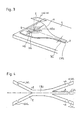
- a transmitted light measuring device shown in FIG. 1 has a semiconductor laser L as the radiation source.
- a diffraction grating G is slidably arranged transversely to its beam direction.
- the semiconductor laser L is arranged, for example, on the bed of a machine tool, not shown.
- the diffraction grating G is arranged, for example, on the carriage of this machine tool, which is also not shown.
- the relative movement between the bed and the sled should be measured as a machine movement. This relative movement corresponds to the relative displacement between the semiconductor laser L and the diffraction grating G.
- the radiation from the semiconductor laser L is diffracted at the diffraction grating G and partial beams + m and -m of the same order but with opposite signs are formed.
- the partial beams + m and -m fall on a substrate S, which is also firmly connected to the machine bed, not shown.
- a substrate S On the substrate S there are two coupling elements + H and -H, two optical fibers + LWL and -LWL, a coupler TBJ and three detectors + D, D, -D.
- these elements are combined in the form of an integrated optical circuit on the substrate S.
- FIG. 2 shows a largely identical arrangement as shown in FIG. 1, but the semiconductor laser L is located on the same side of the diffraction grating G as the substrate S. In this case one speaks of an incident light measuring device. Since the components shown correspond to those in FIG. 1, the same reference symbols are used.
- the partial beams + m and -m strike the coupling elements, which are designed as coupling grids + HG and -HG in the form of horns + H and -H.
- the horns can be used as a kind of plane. Funnels are considered with which large light rays can be coupled in, which are then bundled with the help of constrictions. It is known in principle from EP-B1-0 006 052 to introduce light into waveguides of integrated optical circuits with the aid of coupling-in gratings.
- horns are used in the subject of the application for manufacturing reasons and therefore also for cost reasons, since they can be easily constructed and manufactured nen. Their optical efficiency is also sufficient.
- the shape of the horns + H and -H is parabolic in the broadest sense and is calculated according to the optical and geometric conditions such as the position of the coupling grating + HG or -HG within the respective horn + H or -H, its diffraction structure, the direction and the wavelength of the incident collimated light, etc.
- a horn H is shown schematically on a substrate S. It can also be seen that the constriction ends in an optical waveguide, which is also designed with integrated optics.
- the coupling grating HG it can be said that its axis HGa is at a certain angle to the axis Y of the horn H, which in turn depends on the aforementioned optical and geometric conditions.
- the coupling grating HG are the plane E of the wavefront of the two partial beams + m (-m), the axis HGa of the coupling grating HG, the division g of the coupling grating HG and the propagation fronts We and Wi of the light wave in a plane of the horn H and the optical waveguide FO shown schematically.
- Figure 4 shows schematically a so-called 2 x 3 coupler, which is also referred to as "three-branch junction".
- the theory of such couplers - there, however, of a 3 x 2 coupler - is described in an article by William K. Burns and A. Fenner Milton: "3 x 2 Channel Waveguide Gyroscope Couplers: Theroy” IEEE Journal of Quantum Electronics, Vol. QE- 18, No. 10, Oct. 1982.
- the coupled partial beams + m and -m are fed into the inputs + E and -E of the coupler TBJ by the optical fibers + LWL and -LWL and are brought to interference there.
- the coupler TBJ can be designed so that phase-shifted signals are present at its three outputs + A, A, -A.
- the signals can each be 120 ° out of phase with one another, but signals can also be present at two outputs + A and -A, which represent a sine or cosine function, a reference signal being present at the third output A.
- the signals at the outputs + A, A, -A are in turn guided by means of optical fibers LWL (see FIGS. 1 and 2) to detectors + D, D, -D, from which they are converted into electrical signals and fed to an electronic evaluation circuit.
- the displacement movements of the diffraction grating G are thus transformed into generally digitally displayed position measurement values for the machine movements to be measured.
Landscapes
- Physics & Mathematics (AREA)
- General Physics & Mathematics (AREA)
- Engineering & Computer Science (AREA)
- Microelectronics & Electronic Packaging (AREA)
- Optics & Photonics (AREA)
- Chemical & Material Sciences (AREA)
- Chemical Kinetics & Catalysis (AREA)
- Electrochemistry (AREA)
- General Chemical & Material Sciences (AREA)
- Length Measuring Devices By Optical Means (AREA)
- Optical Transform (AREA)
- Vehicle Body Suspensions (AREA)
- Body Structure For Vehicles (AREA)
- Forklifts And Lifting Vehicles (AREA)
- Eye Examination Apparatus (AREA)
Priority Applications (1)
| Application Number | Priority Date | Filing Date | Title |
|---|---|---|---|
| AT87106621T ATE52328T1 (de) | 1986-07-26 | 1987-05-07 | Lichtelektrische positionsmesseinrichtung. |
Applications Claiming Priority (2)
| Application Number | Priority Date | Filing Date | Title |
|---|---|---|---|
| DE3625327A DE3625327C1 (de) | 1986-07-26 | 1986-07-26 | Lichtelektrische Positionsmesseinrichtung |
| DE3625327 | 1986-07-26 |
Publications (3)
| Publication Number | Publication Date |
|---|---|
| EP0254823A2 EP0254823A2 (de) | 1988-02-03 |
| EP0254823A3 EP0254823A3 (en) | 1989-07-26 |
| EP0254823B1 true EP0254823B1 (de) | 1990-04-25 |
Family
ID=6306044
Family Applications (1)
| Application Number | Title | Priority Date | Filing Date |
|---|---|---|---|
| EP87106621A Expired - Lifetime EP0254823B1 (de) | 1986-07-26 | 1987-05-07 | Lichtelektrische Positionsmesseinrichtung |
Country Status (6)
| Country | Link |
|---|---|
| US (1) | US4938595A (enExample) |
| EP (1) | EP0254823B1 (enExample) |
| JP (1) | JPS6337203A (enExample) |
| AT (1) | ATE52328T1 (enExample) |
| DE (3) | DE3625327C1 (enExample) |
| ES (2) | ES2015555B3 (enExample) |
Families Citing this family (24)
| Publication number | Priority date | Publication date | Assignee | Title |
|---|---|---|---|---|
| DE8717558U1 (de) * | 1987-02-21 | 1989-02-23 | Dr. Johannes Heidenhain Gmbh, 8225 Traunreut | Lichtelektrische Positionsmeßeinrichtung |
| US5070488A (en) * | 1988-06-29 | 1991-12-03 | Atsuko Fukushima | Optical integrated circuit and optical apparatus |
| DE3836703A1 (de) * | 1988-10-28 | 1990-05-03 | Heidenhain Gmbh Dr Johannes | Winkelmesseinrichtung |
| DE3901534C1 (enExample) * | 1989-01-20 | 1990-04-26 | Dr. Johannes Heidenhain Gmbh, 8225 Traunreut, De | |
| DE3918726C1 (enExample) * | 1989-06-08 | 1991-01-10 | Dr. Johannes Heidenhain Gmbh, 8225 Traunreut, De | |
| GB2239088B (en) * | 1989-11-24 | 1994-05-25 | Ricoh Kk | Optical movement measuring method and apparatus |
| DE58905184D1 (de) * | 1989-12-23 | 1993-09-09 | Heidenhain Gmbh Dr Johannes | Einrichtung mit wenigstens einem wellenleiterkoppler. |
| DE58907622D1 (de) * | 1989-12-23 | 1994-06-09 | Heidenhain Gmbh Dr Johannes | Positionsmesseinrichtung. |
| DE4006365A1 (de) * | 1990-03-01 | 1991-10-17 | Heidenhain Gmbh Dr Johannes | Positionsmesseinrichtung |
| DE4007968A1 (de) * | 1990-03-13 | 1991-09-19 | Heidenhain Gmbh Dr Johannes | Optische vorrichtung |
| DE4011718A1 (de) * | 1990-04-11 | 1991-10-17 | Heidenhain Gmbh Dr Johannes | Integriert-optische sensoreinrichtung |
| DE4013566A1 (de) * | 1990-04-27 | 1991-11-07 | Heidenhain Gmbh Dr Johannes | Winkelmesseinrichtung |
| DE4113046C2 (de) * | 1991-04-22 | 1994-02-10 | Zeiss Carl Jena Gmbh | Optoelektronisches Positionsmeßgerät |
| ATE108897T1 (de) * | 1991-05-24 | 1994-08-15 | Heidenhain Gmbh Dr Johannes | Vorrichtung zum ein- und/oder auskoppeln von lichtstrahlen mit einem integriert-optischen baustein. |
| DE4302313C2 (de) * | 1993-01-28 | 1996-12-05 | Heidenhain Gmbh Dr Johannes | Mehrkoordinaten-Meßeinrichtung |
| DE59302118D1 (de) * | 1993-05-21 | 1996-05-09 | Heidenhain Gmbh Dr Johannes | Lichtelektrische Positionsmesseinrichtung |
| US5555470A (en) * | 1993-10-12 | 1996-09-10 | The Regents Of The University Of Michigan | Single wave linear interferometric force transducer |
| DE19917950A1 (de) | 1999-04-21 | 2000-10-26 | Heidenhain Gmbh Dr Johannes | Integrierter optoelektronischer Dünnschichtsensor und Verfahren zu dessen Herstellung |
| DE10013725A1 (de) * | 2000-03-21 | 2001-10-11 | Hannover Laser Zentrum | Meßvorrichtung sowie Verfahren zur Messung eines Weges bei einer Relativbewegung zwischen der Meßvorrichtung und einem Maßstab, der eine Meßspur mit einem Beugungsgitter aufweist, sowie miniaturisierter optischer Abtastkopf |
| DE10058239B4 (de) | 2000-11-17 | 2012-01-26 | Dr. Johannes Heidenhain Gmbh | Positionsmeßeinrichtung |
| US8699836B2 (en) * | 2009-07-07 | 2014-04-15 | Alcatel Lucent | Optical coupler |
| KR200470341Y1 (ko) * | 2012-09-10 | 2013-12-09 | 오창준 | 과채류 접목용 접목 클립 |
| JP6236139B1 (ja) * | 2016-12-08 | 2017-11-22 | 藤森工業株式会社 | 詰め替え容器の注出用スパウト及び包装容器の注出ユニットとの連結構造 |
| CN112097644B (zh) * | 2020-08-24 | 2021-12-17 | 中国科学院长春光学精密机械与物理研究所 | 拼接光栅位移测量系统及测量方法 |
Family Cites Families (14)
| Publication number | Priority date | Publication date | Assignee | Title |
|---|---|---|---|---|
| JPS4835017B1 (enExample) * | 1968-10-02 | 1973-10-25 | ||
| DE2229996A1 (de) * | 1972-06-20 | 1974-01-10 | Leitz Ernst Gmbh | Fotoelektrischer schrittgeber fuer laengen- und winkelmessung |
| GB1443220A (en) * | 1972-12-19 | 1976-07-21 | Leitz Ernst Gmbh | Photo-electric incremental transducer |
| FR2426922A1 (fr) * | 1978-05-26 | 1979-12-21 | Thomson Csf | Structure optique compacte a source integree |
| US4180704A (en) * | 1978-06-28 | 1979-12-25 | International Business Machines Corporation | Detection circuit for a bi-directional, self-imaging grating detector |
| GB2043240A (en) * | 1979-03-01 | 1980-10-01 | Post Office | Improvements in or relating to the switching of signals |
| FR2504256A1 (fr) * | 1981-04-16 | 1982-10-22 | Euromask | Procede et dispositif de mesure optique de deplacement et application aux photorepeteurs sur tranche |
| US4445780A (en) * | 1982-03-01 | 1984-05-01 | The United States Of America As Represented By The Secretary Of The Navy | Fiber optic rotation-sensing gyroscope with (3×2) coupler |
| DE3316144A1 (de) * | 1982-05-04 | 1983-11-10 | Canon K.K., Tokyo | Verfahren und vorrichtung zum messen des ausmasses einer bewegung |
| JPS59164914A (ja) * | 1983-03-10 | 1984-09-18 | Yokogawa Hokushin Electric Corp | 光学式スケ−ル読取装置 |
| US4629886A (en) * | 1983-03-23 | 1986-12-16 | Yokogawa Hokushin Electric Corporation | High resolution digital diffraction grating scale encoder |
| FR2546309B1 (fr) * | 1983-05-19 | 1986-07-04 | Yi Yan Alfredo | Structure de guidage optique utilisant un reseau de diffraction |
| DD221828A1 (de) * | 1983-09-01 | 1985-05-02 | Zeiss Jena Veb Carl | Einrichtung zur fotoelektrischen abtastung von teilungen im auflicht |
| DE3536497A1 (de) * | 1984-10-16 | 1986-04-17 | Mitsubishi Denki K.K., Tokio/Tokyo | Vorrichtung zur erfassung von fokussierungsfehlern in einer kopfanordnung fuer optische scheiben |
-
1986
- 1986-07-26 DE DE3625327A patent/DE3625327C1/de not_active Expired
-
1987
- 1987-02-21 DE DE3705653A patent/DE3705653C1/de not_active Expired
- 1987-05-07 AT AT87106621T patent/ATE52328T1/de not_active IP Right Cessation
- 1987-05-07 DE DE8787106621T patent/DE3762455D1/de not_active Expired - Fee Related
- 1987-05-07 EP EP87106621A patent/EP0254823B1/de not_active Expired - Lifetime
- 1987-05-07 ES ES87106621T patent/ES2015555B3/es not_active Expired - Lifetime
- 1987-07-24 JP JP62183797A patent/JPS6337203A/ja active Granted
- 1987-07-24 US US07/077,190 patent/US4938595A/en not_active Expired - Fee Related
- 1987-12-19 ES ES87118905T patent/ES2019926B3/es not_active Expired - Lifetime
Also Published As
| Publication number | Publication date |
|---|---|
| JPS6337203A (ja) | 1988-02-17 |
| US4938595A (en) | 1990-07-03 |
| JPH0579122B2 (enExample) | 1993-11-01 |
| ES2019926B3 (es) | 1991-07-16 |
| DE3705653C1 (en) | 1988-07-28 |
| DE3762455D1 (de) | 1990-05-31 |
| EP0254823A3 (en) | 1989-07-26 |
| DE3625327C1 (de) | 1988-02-18 |
| ES2015555B3 (es) | 1990-09-01 |
| ATE52328T1 (de) | 1990-05-15 |
| EP0254823A2 (de) | 1988-02-03 |
Similar Documents
| Publication | Publication Date | Title |
|---|---|---|
| EP0254823B1 (de) | Lichtelektrische Positionsmesseinrichtung | |
| DE3942385B4 (de) | Beugungsgitter-Verschiebungsmeßgerät | |
| EP0276395B1 (de) | Lichtelektrische Messeinrichtung | |
| EP0425726B1 (de) | Positionsmesseinrichtung | |
| EP0054292A2 (de) | Faseroptische Messeinrichtung | |
| DE69407208T2 (de) | Optisches Instrument und Verfahren zur Verschiebungsmessung einer Skala | |
| EP0401654B1 (de) | Vorrichtung zum Ein- und/oder Auskoppeln von Lichtstrahlen mit einem integriert-optischen Baustein | |
| DE102010003157A1 (de) | Vorrichtung zur interferentiellen Abstandsmessung | |
| DE102015218539A1 (de) | Optische Positionsmesseinrichtung | |
| EP0625690B1 (de) | Lichtelektrische Positionsmesseinrichtung | |
| EP2816316B1 (de) | Interferometer | |
| EP3258220B1 (de) | Optische positionsmesseinrichtung | |
| EP0365806A2 (de) | Winkelmesseinrichtung | |
| DE3933983A1 (de) | Schaltungsanordnung zur signalinterpolation und versetzungsmesseinrichtung mit der schaltungsanordnung | |
| EP1068486B1 (de) | Positionsmesseinrichtung | |
| EP0608758A1 (de) | Mehrkoordinaten-Messeinrichtung | |
| EP0279944A2 (de) | Lichtelektrische Positionsmesseinrichtung | |
| EP0434855A1 (de) | Positionsmesseinrichtung | |
| EP2869034B1 (de) | Vorrichtung zur Positionsbestimmung | |
| EP0206223B1 (de) | Einrichtung zur Messung der Drehgeschwindigkeit | |
| DE3929794C2 (enExample) | ||
| DE8620094U1 (de) | Lichtelektrische Positionsmeßeinrichtung | |
| DE4113046C2 (de) | Optoelektronisches Positionsmeßgerät | |
| DE102004032016B4 (de) | Fabry-Pérot-Faserinterferometer | |
| DE19916754A1 (de) | Vorrichtung zur optischen Datenübertragung |
Legal Events
| Date | Code | Title | Description |
|---|---|---|---|
| PUAI | Public reference made under article 153(3) epc to a published international application that has entered the european phase |
Free format text: ORIGINAL CODE: 0009012 |
|
| 17P | Request for examination filed |
Effective date: 19870516 |
|
| AK | Designated contracting states |
Kind code of ref document: A2 Designated state(s): AT CH DE ES FR GB IT LI NL SE |
|
| PUAL | Search report despatched |
Free format text: ORIGINAL CODE: 0009013 |
|
| AK | Designated contracting states |
Kind code of ref document: A3 Designated state(s): AT CH DE ES FR GB IT LI NL SE |
|
| 17Q | First examination report despatched |
Effective date: 19891013 |
|
| ITF | It: translation for a ep patent filed | ||
| GRAA | (expected) grant |
Free format text: ORIGINAL CODE: 0009210 |
|
| AK | Designated contracting states |
Kind code of ref document: B1 Designated state(s): AT CH DE ES FR GB IT LI NL SE |
|
| REF | Corresponds to: |
Ref document number: 52328 Country of ref document: AT Date of ref document: 19900515 Kind code of ref document: T |
|
| ET | Fr: translation filed | ||
| RAP4 | Party data changed (patent owner data changed or rights of a patent transferred) |
Owner name: DR. JOHANNES HEIDENHAIN GMBH |
|
| GBT | Gb: translation of ep patent filed (gb section 77(6)(a)/1977) | ||
| REF | Corresponds to: |
Ref document number: 3762455 Country of ref document: DE Date of ref document: 19900531 |
|
| PLBE | No opposition filed within time limit |
Free format text: ORIGINAL CODE: 0009261 |
|
| STAA | Information on the status of an ep patent application or granted ep patent |
Free format text: STATUS: NO OPPOSITION FILED WITHIN TIME LIMIT |
|
| 26N | No opposition filed | ||
| ITTA | It: last paid annual fee | ||
| EAL | Se: european patent in force in sweden |
Ref document number: 87106621.3 |
|
| PGFP | Annual fee paid to national office [announced via postgrant information from national office to epo] |
Ref country code: GB Payment date: 19990413 Year of fee payment: 13 |
|
| PGFP | Annual fee paid to national office [announced via postgrant information from national office to epo] |
Ref country code: FR Payment date: 19990419 Year of fee payment: 13 |
|
| PGFP | Annual fee paid to national office [announced via postgrant information from national office to epo] |
Ref country code: SE Payment date: 19990421 Year of fee payment: 13 Ref country code: CH Payment date: 19990421 Year of fee payment: 13 |
|
| PGFP | Annual fee paid to national office [announced via postgrant information from national office to epo] |
Ref country code: AT Payment date: 19990422 Year of fee payment: 13 |
|
| PGFP | Annual fee paid to national office [announced via postgrant information from national office to epo] |
Ref country code: NL Payment date: 19990427 Year of fee payment: 13 |
|
| PGFP | Annual fee paid to national office [announced via postgrant information from national office to epo] |
Ref country code: ES Payment date: 19990519 Year of fee payment: 13 |
|
| PG25 | Lapsed in a contracting state [announced via postgrant information from national office to epo] |
Ref country code: GB Free format text: LAPSE BECAUSE OF NON-PAYMENT OF DUE FEES Effective date: 20000507 Ref country code: AT Free format text: LAPSE BECAUSE OF NON-PAYMENT OF DUE FEES Effective date: 20000507 |
|
| PG25 | Lapsed in a contracting state [announced via postgrant information from national office to epo] |
Ref country code: SE Free format text: LAPSE BECAUSE OF NON-PAYMENT OF DUE FEES Effective date: 20000508 Ref country code: ES Free format text: THE PATENT HAS BEEN ANNULLED BY A DECISION OF A NATIONAL AUTHORITY Effective date: 20000508 |
|
| PG25 | Lapsed in a contracting state [announced via postgrant information from national office to epo] |
Ref country code: LI Free format text: LAPSE BECAUSE OF NON-PAYMENT OF DUE FEES Effective date: 20000531 Ref country code: CH Free format text: LAPSE BECAUSE OF NON-PAYMENT OF DUE FEES Effective date: 20000531 |
|
| PG25 | Lapsed in a contracting state [announced via postgrant information from national office to epo] |
Ref country code: NL Free format text: LAPSE BECAUSE OF NON-PAYMENT OF DUE FEES Effective date: 20001201 |
|
| GBPC | Gb: european patent ceased through non-payment of renewal fee |
Effective date: 20000507 |
|
| REG | Reference to a national code |
Ref country code: CH Ref legal event code: PL |
|
| EUG | Se: european patent has lapsed |
Ref document number: 87106621.3 |
|
| PG25 | Lapsed in a contracting state [announced via postgrant information from national office to epo] |
Ref country code: FR Free format text: LAPSE BECAUSE OF NON-PAYMENT OF DUE FEES Effective date: 20010131 |
|
| NLV4 | Nl: lapsed or anulled due to non-payment of the annual fee |
Effective date: 20001201 |
|
| REG | Reference to a national code |
Ref country code: FR Ref legal event code: ST |
|
| PGFP | Annual fee paid to national office [announced via postgrant information from national office to epo] |
Ref country code: DE Payment date: 20010509 Year of fee payment: 15 |
|
| REG | Reference to a national code |
Ref country code: ES Ref legal event code: FD2A Effective date: 20020204 |
|
| PG25 | Lapsed in a contracting state [announced via postgrant information from national office to epo] |
Ref country code: DE Free format text: LAPSE BECAUSE OF NON-PAYMENT OF DUE FEES Effective date: 20021203 |
|
| PG25 | Lapsed in a contracting state [announced via postgrant information from national office to epo] |
Ref country code: IT Free format text: LAPSE BECAUSE OF NON-PAYMENT OF DUE FEES;WARNING: LAPSES OF ITALIAN PATENTS WITH EFFECTIVE DATE BEFORE 2007 MAY HAVE OCCURRED AT ANY TIME BEFORE 2007. THE CORRECT EFFECTIVE DATE MAY BE DIFFERENT FROM THE ONE RECORDED. Effective date: 20050507 |