EP0250081A2 - Réseau mémoire à plusieurs portes - Google Patents
Réseau mémoire à plusieurs portes Download PDFInfo
- Publication number
- EP0250081A2 EP0250081A2 EP87304170A EP87304170A EP0250081A2 EP 0250081 A2 EP0250081 A2 EP 0250081A2 EP 87304170 A EP87304170 A EP 87304170A EP 87304170 A EP87304170 A EP 87304170A EP 0250081 A2 EP0250081 A2 EP 0250081A2
- Authority
- EP
- European Patent Office
- Prior art keywords
- signal
- providing
- response
- match
- transition
- Prior art date
- Legal status (The legal status is an assumption and is not a legal conclusion. Google has not performed a legal analysis and makes no representation as to the accuracy of the status listed.)
- Granted
Links
Images


Classifications
-
- G—PHYSICS
- G11—INFORMATION STORAGE
- G11C—STATIC STORES
- G11C8/00—Arrangements for selecting an address in a digital store
- G11C8/16—Multiple access memory array, e.g. addressing one storage element via at least two independent addressing line groups
-
- G—PHYSICS
- G06—COMPUTING; CALCULATING OR COUNTING
- G06F—ELECTRIC DIGITAL DATA PROCESSING
- G06F13/00—Interconnection of, or transfer of information or other signals between, memories, input/output devices or central processing units
- G06F13/14—Handling requests for interconnection or transfer
- G06F13/16—Handling requests for interconnection or transfer for access to memory bus
- G06F13/18—Handling requests for interconnection or transfer for access to memory bus based on priority control
Definitions
- the present invention relates generally to integrated circuit memory devices comprising an array of memory locations and further comprising multiple ports for receiving multiple combinations of binary address signals to simultaneously address multiple locations of the array and more particularly to integrated circuit memory devices including means for controlling a simultaneous provision of a combination of binary address signals to more than one port.
- a multiprocessor system 18 comprising a dual port memory device 20 and two respective microprocessors 22 and 24.
- the memory device 20 includes a left port for receiving left port binary address signals at terminals labelled AOL-A9L and left port binary input/output data signals at terminals labelled DOL-D7L. It also includes a right port for receiving right port binary address signals at terminals labelled AOR-A9R and right port binary input/output data signals labelled DOR-D7R.
- the left port receives address and data signals from the first microprocessor 22, and the right port receives address and data signals from the second microprocessor 24.
- the memory array 20 further includes respective left and right status signal terminals labelled respectively BUSYL and BUSVR which are discussed further below.
- Typical earlier memory arrays of the general type illustrated in Fig. 1 included contention logic circuitry (not shown) used to arbitrate access to a respective memory location when more than one microprocessor simultaneously sought access to that location.
- the contention logic circuitry often compared the combinations of address signals provided to the respective left and right address terminals AOL-A9L and _AOR-A9R in order to determine whether there was a simultaneous attempt to access a single memory location of the memory array 20.
- the contention logic circuitry would determine which of the microprocessors 22 or 24 seeking to access the memory location would be provided first access to the location.
- the circuitry then provided, on a respective left or right status signal terminal, an active status signal, to a microprocessor whose access was to be delayed.
- a microprocessor granted first access then proceeded with its task; while a microprocessor whose access was delayed, for example, awaited access.
- the first microprocessor 22 might momentarily provide to the left port address terminals AOL-A9L a combination of binary address signals corresponding to a first location and then provide a. combination of address signals corresponding to a second location.
- the second microprocessor 24 might provide to the right port address terminals AOR-A09 a combination of binary address signals which correspond to a third location, and then after a short period of time may provide a combination of address signals which correspond to the first location (where the first, second and third locations are distinct).
- an active status signal erroneously may be provided to either one or the other of the microprocessors 22 or 24 and incorrectly indicate a temporary match in address signal combinations.
- Address signal skew can result when signals comprising a combination of signals provided to the left port, for example, change logical states at slightly different points in time. For example, in changing from a combination of address signals corresponding to one location to a combination corresponding to another location, it. may be necessary to change the logical states of both the signals provided to terminal AOR and to terminal A9R. However, the signal provided to AOR, for example, might not change its logical state until five nanoseconds after the signal provided to A9R has changed its logical state.
- the five nanosecond delay would represent address signal skew which sometimes can result in a temporary match in combinations of address signals provided to the respective left and right ports, and consequently, may result in the provision of an active status signal which unnecessarily can delay access to the memory array 20 by one of the microprocessors 22 or 24.
- the present invention provides an integrated circuit device including a memory array comprising a plurality of respective memory locations for storing binary data. Each respective location of the array can be addressed by providing a combination of binary address signals which corresponds to the addressed location.
- the device includes at least two ports for receiving combinations of binary address signals.
- Transition detection and signal providing circuitry are included for detecting a change in a respective binary address signal combination received by either a first or second of the at least two ports.
- the transition detection and signal providing circuitry provides a first transition signal in response to a change in a respective first combination of binary address signals received by the first port and provides a second respective transition signal in response to a change in a respective second combination of binary address signals. received by said second port.
- contention detection and signal providing circuitry is included for receiving the first and second transition signals and for detecting a match in the first and second combinations of binary address signals.
- the contention detection and signal providing circuitry provides a respective first status signal in an inactive state in response to the first transition signal and provides a respective second status signal in an inactive state in response to the second transition signal.
- the present invention also provides a method for controlling access to respective ports of a multiple port integrated circuit memory array including a plurality of respective memory locations, each memory location corresponding to a respective combination of binary address signals.
- the method includes the step of receiving a first combination of binary address signals and a second combination of binary address signals. It further includes the steps of detecting a change in the first combination and of detecting a change in the second combination. A first transition signal is provided in response to a change in the first combination, and a second transition signal is provided in response to a change in the second combination.
- the method further includes the step of determining whether there is a match in the first and second combinations of binary address signals and providing a match signal in response to a match. Substantially during a first period of time, a first status signal is provided in an inactive state in response to the first transition signal, and substantially during a second period of time, a second status signal is provided in an inactive state in response to the second transition signal.
- the present invention advantageously provides a device and an associated method which are more tolerant to near matches and to very brief temporary matches of address signal combinations provided to different ports of a multiple port memory array without providing a status signal which unnecessarily delays access to the array.
- the present invention comprises a novel integrated circuit device and an associated method.
- the device includes a memory array comprising a plurality of respective memory locations for storing binary data, each respective memory location corresponding to a respective combination of binary address signals.
- the memory 26 includes a dual port 1024 X 8 random-access memory array 28 including respective left and right row decoder drivers 30 and 32 and respective left and right column decoder and input/output circuits 34 and 36.
- the memory 26 also includes integrated contention logic circuitry 38 coupled as shown.
- the preferred embodiment described herein includes a 1024 x 8 array, arrays of other sizes can be used as well.
- the preferred embodiment includes a static random access memory array, other types of memory devices could be provided in accordance with the principles of the invention.
- a left port of the dual port static random-access memory 26 is coupled to receive- a combination of ten binary address signals.
- Seven binary address signals LAO-LA6 are provided to the left row decoder driver 30, and three binary address signals ' LA7-LA9 are provided to the left column decoder and input/output circuitry 34.
- Each respective combination of ten binary address signals LAO-LA9 provided to the left port of the dual port RAM memory array 28 corresponds to a respective location of the array 28.
- Eight-bit data words alternatively can be written into an addressed location of the array 28 or read out of an addressed location of the array 28 by the left row decoder 30, and left column decoder and input/output circuitry 34 on appropriate lines labelled L I/O.
- each respective combination of ten binary address signals RAO-RA9 provided to a right port of the dual port RAM array 28 corresponds to a respective location of the array 28.
- An addressed location of the array 28 can be accessed for either writing of eight-bit data words into the location or reading eight-bit data words from the location via the right row decoder 32 and the right column decoder and input/output circuitry 36 on appropriate lines labelled R-I/O.
- Each respective binary address signal LAO-LA6 provided to'the left row decoder driver 30 and each respective binary address signal LA7-LA9 provided to the left column decoder and input/output circuitry 34 also is provided to the contention logic circuitry 38
- each respective binary address signal RAO-RA6 provided to the right row decoder driver 32 and each respective binary address signal RA7-RA9 provided to the right column decoder and input/output circuitry 36 also is provided to the contention logic circuitry 38.
- the contention logic circuitry 38 provides a number of status signals on respective lines 40-50 which are discussed below and receives on respective lines 54 and 56 respective signals which either enable or disable the respective left and right ports of the RAM array 28 as discussed more fully below.
- the dual port static random-access memory 26 receives a first combination of binary address signals LAO-LA9 provided to its left port and receives a second combination of binary address signals RA0-RA9 provided to its right port.
- first combination of address signals LAO-LA9 to the left port
- second combination of address signals RAO-RA9 to the right port
- two different locations of the RAM array 28 simultaneously can be addressed-
- the dual port static random-access memory 26 simultaneously can provide access to its RAM array 28 by multiple microprocessors (not shown).
- the contention logic circuitry 38 monitors the respective combinations of binary address signals LAO-LA9 and RAO-RA9 in order to determine when the respective combinations correspond to a single location in the array 28. In the event that respective combinations of binary signals match and, therefore, do correspond to a single location of the array 28, the contention logic circuitry 38 detects the match, and determines which port should receive first access to the particular location and provides appropriate status signals as discussed below. In accordance with the present invention, however, the contention logic circuitry' 38 substantially reduces the provision of status signals which unnecessarily limit access to an addressed memory location.
- the contention logic circuitry 38 is shown to include ten respective buffer circuits 55 each coupled to receive a respective left address signal LAO-LA9.
- the circuitry 38 further includes left row address signal transition detection circuitry (LRT) 58 and left column address signal transition detection circuitry (LCT) 60.
- LRT left row address signal transition detection circuitry
- LCT left column address signal transition detection circuitry
- the LRT 58 is coupled to receive seven buffered binary address signals LAO-LA6, and the LCT 60 is coupled to receive three buffered binary address signals LA7-LA9.
- the LRT 58 comprises circuitry which also can be used to provide bit line precharge signals and data line equalization signals.
- the LCT 60 comprises circuitry which also can be used to provide data line equalization signals.
- the LRT 58 is further coupled by branched line 62 to a left transition signal generator 64 and by branched line 62 to a port priority circuit 74.
- the LCT 60 also is further coupled by branched line 66 to the left transition signal generator 64 and by branched line 66 to the port priority circuit 74.
- the left transition signal generator 64 is coupled by line 68 to a left status signal generator 70.
- the left status signal generator 70 is coupled by line 72 to a port priority circuit 74, and is coupled by branched line 76 to a comparator circuit 78.
- the left status signal generator 70 also is coupled to a logical level 1 signal by line 80.
- the contention logic circuitry 38 also includes ten respective buffer circuits 57 each coupled to receive a respective right address signal RAO-RA9.
- the circuitry 38 further includes right row address signal transition circuitry (RRT) 82 and right column address signal transition detection circuitry (RCT) 84.
- the RRT 82 is coupled to receive seven buffered binary address signals RAO-RA6, and the RCT is coupled to receive three buffered binary address signals RA7-RA9.
- the RRT 82 comprises circuitry which also can be used to provide bit line precharge signals and data line equalization signals.
- the RCT 84 comprises circuitry which also can be used to provide data line equalization signals.
- the RRT 82 is further coupled by branched line 86 to right transition signal generator 88 and by branched line 86 to the port priority circuit 74.
- the RCT 84 also is further coupled by branched line 90 to the right transition signal generator 88 and by branched line 90 to the port priority circuit 74.
- the right transition signal generator 88 is coupled by line 92 to a right status signal generator 94.
- the right status signal generator 94 is coupled by line 96 to the port priority circuit 74 and is coupled by branch line 76 to the comparator circuit 78: Also, the right status generator 94 is coupled by line 98 to a logical level 1 signal.
- the comparator circuit 78 receives each of the binary address signals LAO-LA9 provided to the left port and receives each of the binary address signals RAO-RA9 provided to the right port.
- the respective large arrow labelled 100 represents the reception by the comparator circuit 78 of binary signals LAO-LA9
- the large arrow labelled 102 represents the reception by the comparator circuit 78 of binary signals RAO-RA9.
- the LRT 58 detects substantially any change in a logical state of any one or more of the buffered signals LAO-LA6 provided to it, and in response to any such change in any one or more of those signals, it provides on line 62 a first left port address change pulse signal ( ⁇ 1>1 L) in a logical level 1 state.
- the LCT 60 detects substantially any change in a logical state of any one or more of the buffered signals LA7-LA9 provided to it, and in response to such a change, provides on line 66 a second left port address change pulse signal (02L) in a logical level 1 state.
- the respective first and second left port address change pulse signals, 01 L and 02L, provided on lines 62 and 66 are received by the left transition signal generator 64.
- the left transition signal generator 64 In response to a logical level 1 address change signal received on either line 62 or line 66 or both, the left transition signal generator 64 provides on lines 68 a logical level 1 first transition signal ( O T1).
- the O T1 signal is provided on line 68 to the left status signal generator 70.
- the RRT 82 detects substantially any change in a logical state of any one or more of the buffered signals RAO-RA6 provided to it, and in response to any such change, provides on line 86 a first left port address change pulse signal ( ⁇ 1R) in a logical level 1 state as will be described more fully below.
- the RCT 84 detects substantially any change in a logical state of any one or more of the three buffered address signals RA7-RA9 provided to it, and in response to such a change, provides on line 90 a second left port address change pulse signal ( 0 2R) in a logical level 1 state.
- the respective first and second right address change pulse signals, ⁇ 1R and ⁇ 2R, provided on lines 86 and 90, are received by the right transition signal generator 88.
- the right transition signal generator 88 In response to a logical 1 state address change signal received on either line 86 or 90 or both, the right transition signal generator 88 provides on line 92 a logical level 1 second transition signal ( ⁇ T2).
- the 4 T2 signal is provided on line 92 to the right status signal generator 94.
- the comparator 78 receives a combination of buffered signals substantially identical to those received by the left port of the RAM array 28 and to those received by the right port of the RAM array 28.
- the comparator circuit 78 continually monitors the combinations of binary address signals, LAO-LA9 and RAO-RA9, provided to the respective left and right ports of the RAM array 28 and generates on line 76 a logical state 0 address match signal ( AM) in response to a match in each respective signal of the combinations and a logical state 1
- AM on line 76 indicates when there is a match of combinations of binary address signals. It will be appreciated, of course, that such a match occurs when, for example, two microprocessors (not shown) simultaneously seek access to a single location of the RAM array 28.
- the port priority circuit 74 provides on lines 72 and 96 respective priority signals which determine whether the left status signal generator 70 will provide appropriate signals on lines 40-44 which substantially delay access to the left port of the RAM array 28 in response to a logical state 0 AM signal on line 76; or the right status signal generator 94 will provide on lines 46-50 status signals which substantially delay access to the right port of the RAM array 28 in response to a logical state 0 AM signal on line 76.
- Figure 4 is a circuit diagram showing details of the left transition signal generator 64 which comprises an OR logic gate including a NOR logic section shown within dashed lines 104 and an inverter logic section shown within dashed lines 106.
- the OR logic gate includes six transitor devices connected as shown.
- the NOR logic section includes two enhancement transitor devices 108 and 110, a depletion device 112 and a Z transistor device 114.
- the inverter logic section includes an enhancement transitor device 116 and a depletion transitor device 118.
- the respective enhancement devices 108, 110 and 116 are characterized by voltage thresholds of approximately .8 volts.
- the respective D devices 112 and 118 are characterized by voltage thresholds of approximately -3.5 volts.
- the respective Z device 114 is characterized by a voltage threshold of approximately 0 volts.
- Signal CEL applied to a gate terminal of the Z transitor device 114 is in a logical level 1 state when the left port of the RAM array 28 is enabled.
- Pulse signals ⁇ 1L and ⁇ 2L represent the first and second left address change signals provided on respective lines 62 and 66 by the respective LRT 58 and LCT 60.
- Signal ⁇ T1 represents the first transition signal provided on line 68 in response to either a logical 1 state pulse signal ⁇ 1L or 0 2L.
- the OR logic gate of Fig. 4 is constructed such that a rising leading edge of a logical state 1 O T1 signal substantially coincides in time with a rising leading edge of either a logical 1 state 0 1 L pulse signal or ⁇ 2L pulse signal, whichever rises first, and such that a failing edge of the logical state 1 ⁇ T1 signal is delayed by approximately two nanoseconds after the falling edge of either the logical 1 state ⁇ 1L pulse signal or 0 2L pulse signal, whichever falls last.
- timing of the provision of a ⁇ T1 signal relative to the ⁇ 1L and 42L pulse signals can be varied by varying the current drive ratios of the NOR and inverter logic sections and by appropriately varying the capacitive loading of the NOR and inverter logic sections.
- a circuit diagram illustrating details of the right transition signal generator 88 which comprises an OR logic gate including a NOR logic section shown within dashed lines 120 and an inverter logic section shown within dashed lines 122.
- the NOR logic section includes two enhancement transitor devices 124 and 126, a depletion device 128 and a Z transitor device 130 connected as shown.
- the inverter logic section includes an enhancement transitor device 132 and a depletion transitor device 134 connected as shown.
- the respective enhancement transitor devices 124, 126 and 132 are characterized by threshold voltages of approximately .8 volts.
- the D transistor devices 128 and 134 are characterized by voltage thresholds of approximately -3.5 volts.
- the Z transitor device 130 is characterized by a threshold voltage of approximately 0 volts.
- Signal CER applied to a gate electrode of the Z transitor device 130 is in a logical level 1 state when the right port of the RAM array 28 is enabled.
- Signals ⁇ 1 R and 0 2R represent the first and second right address change signals provided on lines 86 and 90 by the respective RRT .82 and RCT 84.
- Signal ⁇ T2 represents the second transition signal provided on line 92 in response to either a logical 1 state signal ⁇ 1 R or ⁇ 2R.
- the OR logic gate illustrated in Fig. 5 is constructed such that a rising leading edge of a logical level 1 state ⁇ T2 signal substantially coincides in time with a rising leading edge of a first-to-occur pulse signal ⁇ 1 R or 0 2R, and such that a falling edge of a ⁇ T2 logical level 1 state signal lags a last-to-occur falling edge of a ⁇ 1 R or 0 2R pulse signal by approximately two nanoseconds.
- an OR logic gate like that illustrated in Fig. 5 can be constructed with the above-described timing characteristics by proper construction of current drive ratios of the NOR and inverter sections and by providing appropriate capacitive loading to the NOR and inverter sections.
- the comparator circuit 78 comprises ten exclusive OR logic gates 136 and an OR .logic gate 138 connected as shown.
- Each respective exclusive OR logic gate 136 receives a pair of corresponding binary address signals, one of which corresponds to an address signal applied to a left port of the RAM array 28 and another of which corresponds to an 15 address signal provided to the right port of the RAM array 28.
- signal A1 and signal A1R both are provided to one exclusive OR gate 136
- signal A9L and signal A9R both are provided to another exclusive OR gate 136.
- Address match signal AM provided on line 76 by the OR gate 138 takes a logical level 1 state unless there is a match in each of the corresponding pairs of binary address signals provided to the respective left and right ports of the RAM array 28.
- the OR logic gate 138 provides on line 76 address match signal AM in a logical 0 state only when the combination of binary address signals provided to the left and right ports each correspond to a single location of the memory array 28.
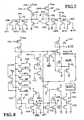
- the drawings of Fig. 7 show a circuit diagram of the port priority circuit 74.
- the port priority circuit 74 includes a latch section indicated generally by the numeral 140 which includes depletion transitor devices 141 and 143 and Z transistor devices 145 and 147 connected as shown. It also includes four left section pull-down enhancement transitors 142, 144, 146 and 148 connected as shown and four right section pull-down transitors labelled 150-156 connected as shown.
- the port priority circuit 74 provides port priority left (PPL) signals on line 72 and provides port priority right (PPR) signals on line 96.
- PPL port priority left
- PPR port priority right
- the respective PPL and PPR signals determine which port of the RAM array 28 will receive first priority in the event that address signals provided to the respective left and right ports of the RAM array 28 simultaneously address a single memory location of the RAM array 28. For example, when the port priority circuit 74 is in a state wherein the PPL signal is in a logical level 1 state and the PPR is in a logical level 0 state, the left port will be provided first access to an address location of the array 28 in the event that a combination of binary address signals provided to the left and right ports of the array 28 simultaneously address a single location.
- signal PPL provided on line 72 generally remains in its latched state whether that be a logical level 1 or 0 state. It will be appreciated that when signals ⁇ 1 L, ⁇ 2L and CEL all are in logic 0 states, then signal PPL provided on line 72 generally remains in its latched state whether that be a logical level 1 or 0 state. It will be appreciated that when signals ⁇ 1 L, ⁇ 2L and CEL all are in logic 0 states, then signal PPL provided on line 72 generally remains in its latched state whether that be a logical level 1 or 0 state. It will be appreciated that when signals ⁇ 1 L, ⁇ 2L and
- the latch circuit section 140 will set such that the priority signal, either PPL or PPR, whose pull-down transitors first return to a condition in which all signals provided to their respective gate electrodes are in a logical level 0 state will take on a logical 1 state, and the other priority signal will remain in a logical level 0 state.
- signals PPL and PPR are in logical level 0 states, and signals ⁇ 1 L, 0 2L, CEL and a signal provided to the gate electrode of transitor 142 all take on a logical level 0 state before signals ⁇ 1 R, 0 2R, CER, and the signal provided to the gate electrode of transitor 150 all take on a logical 0 state, then signal PPL will take on a logical 1 state, and signal PPR will remain in a logical 0 state.
- the left port will have priority in addressing an address location when the combinations of address signals provided to the left and right ports match.
- the' enabled port automatically receives first priority; since only its priority signal is in a logical 1 state. For example, if the right port is not enabled, then signal CER will be in a logical level 0 state, and signal CER provided to the gate electrode of transitor 152 will be in a logical 1 state causing signal PPR to be in a logical level 0 state. Thus, the left port will have priority over the right port.
- pulse signals ⁇ 1 L, ⁇ 2L, ⁇ 1 R and 0 2R generally take on a logical 1 state only for a period of approximately seven to eight nanoseconds following a change in a corresponding combination of address signals. Consequently, a condition in which both signals PPL and PPR simultaneously are in a logical 0 state ordinarily will be relatively short-lived, and generally a port which first experienced a transition in a combination of address signals provided to it will achieve priority over the other port.
- metastable condition may occur in which both signals PPL and PPR remain in approximately logical level 0 states although signal pulses ⁇ 1 L, ⁇ 2L, ⁇ 1 R, 0 2R, 6ER and CEL all are in logical 0 states.
- a metastable condition is an example of a possible but atypical condition in the operation of the port priority circuit 74. It can momentarily result in a simultaneous assertion of active BUSYL and BUSYR signals which are discussed below. Thus, except for the metastable condition, BUSYL and
- BUSYR signals are not simultaneously in active states.
- the left status signal generator 70 which includes a plurality of transitor devices connected as shown.
- the left status signal generator 70 provides three respective status signals EINTL, EWEL and BUSYL, each of which are active low (logical level 0) state signals, on respective lines 40, 42 and 44.
- Signal EINTL is provided to an interrupt buffer (not shown). When signal EINTL is in a logical 1 state (a high state), interrupt flags cannot be set or reset by the left port, and when signal EINTL is in a logical 0 state (a low state) interrupt flags can be set or reset by the left port.
- Signal EWEL is provided to the left column decoder and input/output circuitry 34. When signal EWEL is in a logical 1 state, binary data cannot be written into the memory array 28 by the left port, and when signal
- EWEL is in a logical 0 state
- binary data can be written into the memory array 28 by the left port.
- a microprocessor which forms no part of the present invention and is not shown, coupled to line 44, for example, will have its access to the left port delayed.
- the microprocessor will not have its access to the left port delayed.
- CEINL is an externally generated active low signal which, as illustrated in Fig. 2, is provided to the contention logic circuitry 38 on line 54.
- a logical 0 state CEINL signal provided on line 54 enables the left port of the RAM array 28.
- Signals CEL and CEL are internally generated complementary signals generated in response to signal
- CEINL The logical state of signal CEL is the logical inverse of that of signal CEINL.
- a change in a combination of address signals provided to the buffer circuits 55 coupled to the LCT 60 results in a provision of a logical level 1 state ⁇ 2L pulse signal on branched line 66 after a delay of approximately eight to ten nanoseconds.
- a logical level 1 state ⁇ T1 signal is provided.
- the logical state 1 ⁇ T1 signal remains in a logical level 1 state substantially throughout a period of time during which either or both the ⁇ 1 L or ⁇ 2L pulse signals are in logical level 1 states, and for approximately two nanoseconds after both the ⁇ 1 L and ⁇ 2L pulse signals have transitioned back to logical level 0 states.
- Status signals EINTL, EWEL and BUSYL all take logical level 1 states substantially during an entire period of time during which signal ⁇ T1 is in a logical level 1 state.
- the dashed lines shown in Fig. 9 associated with the three respective status signals indicate that outside a period of time when signal ⁇ T1 is in a logical level 1 state, the logical states of the three status signals can be either logical 1 or logical 0.
- CEINL is provided on line 54 to the contention logic circuitry 38. shown in Fig. 2. It will be appreciated that when signal CEINL is in the logical level 1 (inactive) state, the left port is not enabled, and therefore, address locations of the RAM array 28 cannot be accessed via the left port.
- precharge signals are provided to bit lines of the RAM array 28 in order to prevent access time delays in a next access. Since, in the preferred embodiment, signals ⁇ 1L and 0 2L are derived from such precharge signals and from such data line equalization signals, pulse signals ⁇ 1 L and 0 2L are in logical level 1 states during the time when CEINL is in a logical 1 state. Consequently, signal ⁇ T1 also takes on a logical level 1 state when signal CEINL is in a logical level 1 state.
- Pulse signals ⁇ 1 and 0 2L remain in the logical 1 state substantially until signal CEINL transitions to a logical level 0 state, and the left port once again is enabled.
- the O T1 signal transitions back to the logical level 0 state approximately two nanoseconds after the ⁇ 1 and 0 2L signals both have transitioned back to the logical level 0 state.
- the three status signals EINTL, EWEL and BUSYL all are in logical level 1 states.
- a logical level 0 state (active) BUSYL status signal is provided when four conditions are satisfied: both ports are enabled; there is a match in a combination of address signals provided to respective left and right ports of the RAM array 28; the left port does not have priority; and signal ⁇ T1 is in a logical level 0 state.
- NOR gate 158 a logical level 1 state signal will be provided on line 160 by the NOR gate 158 when the left port is enabled ( CEL is in logical 0 state); and the left port does not have priority (signal PPL is in a logical 0 state); there is an address match (signal
- AM is in logical level 0 state
- the combination of address signals provided to the right port have settled and are steady (pulse signals ⁇ 1 R and ⁇ 2R are in logical level 0 states).
- the provision of a logical level 1 state signal on line 160 to inverter circuit 162 results in the provision of a logical level 0 signal to a gate electrode of transitor 164 of a NOR gate indicated by reference numeral 166.
- a logical level 0 state signal is provided to the gate electrode of transitor 164 and signals
- inverter circuit 168 causes a provision of a logical 1 state signal to a gate electrode of transitor 172, and as a result, a logical level 0 state (active) BUSYL status signal is provided.
- Signal ⁇ T1 when provided in a logical level 1 state by the left transition signal generator 64 to a gate electrode of transitor 174, pulls down the logical level of the signal provided to inverter circuit 168, and ultimately results in a logical level 1 (inactive) state BUSYL status signal being provided on line. 44. Furthermore, disabling of the left port, which results in a provision of a logical level 1 state CEL signal to a gate electrode of transitor 176, similarly results in a provision of a logical level 1 state (inactive) BUSYL status signal.
- signals provided to the NOR logic gate 158 can cause a logical level 0 (active) state
- BUSYL status signal in response to a match in combinations of address signals provided to a respective left and right ports.
- a logical level state ⁇ T1 signal is provided in response to a change in a combination of address signals provided to either the LRT 58 or the LCT 60, the
- BUSYL status signal is held in a logical level 1 (inactive) state.
- the left status signal generator 70 delays a provision of a logical level 0 state (active)
- BUSYL status signals as a result of address signal skew or near matches in combinations of address signals provided to its respective left and right ports.
- a ⁇ T1 signal which remains in a logical level 1 state for a period of time approximately two nanoseconds after the later falling edge of logical level 1 state 01 L and ⁇ 2L signals, substantial ensures that the latch circuit section 140 of the port priority circuit 74 has latched, and signal PPL has stabilized before signal ⁇ T1 transitions back to a logical level 0 state after an address transition, and the BUSYL status signal once again becomes responsive to a signal provided on line 160 by NOR logic gate 158. It will be appreciated, of course, that when the BUSYL status signal is responsive to a signal provided on line 160, the BUSYL status signal is substantially responsive to the address match signal
- the present arrangement and associated method advantageously permits the operation of multiple port integrated circuit memory array devices which better tolerate near matches in combinations of address signals provided to different ports and very brief matches in such signal combinations due to problems such as address signal skew, without causing: status signals which unnecessarily delay access to the memory array of such devices. More particularly, the provision of respective O T1 and ⁇ T2 signals in response to changes in respective binary address signal combinations is used to substantially delay for a prescribed period of time an evaluation by such a device of whether address signal combinations match.
- the prescribed period of time for the left port is when signal ⁇ T1 is in a logical level 1 state, and for the right port, it is when signal ⁇ T2 is in a logical level 1 state.
- the effects of very near matches and of problems such as address signal skew presumably will dissipate, and, therefore, will not result in a provision of a status signal which unnecessarily delays access to the memory array.
Landscapes
- Engineering & Computer Science (AREA)
- Theoretical Computer Science (AREA)
- Microelectronics & Electronic Packaging (AREA)
- Physics & Mathematics (AREA)
- General Engineering & Computer Science (AREA)
- General Physics & Mathematics (AREA)
- Static Random-Access Memory (AREA)
- Use Of Switch Circuits For Exchanges And Methods Of Control Of Multiplex Exchanges (AREA)
- Communication Control (AREA)
- Dram (AREA)
Priority Applications (1)
| Application Number | Priority Date | Filing Date | Title |
|---|---|---|---|
| AT87304170T ATE101934T1 (de) | 1986-05-19 | 1987-05-11 | Mehrfachport-speichernetzwerk. |
Applications Claiming Priority (2)
| Application Number | Priority Date | Filing Date | Title |
|---|---|---|---|
| US06/864,690 US4742493A (en) | 1986-05-19 | 1986-05-19 | Multiple port memory array device including improved timing and associated method |
| US864690 | 1986-05-19 |
Publications (3)
| Publication Number | Publication Date |
|---|---|
| EP0250081A2 true EP0250081A2 (fr) | 1987-12-23 |
| EP0250081A3 EP0250081A3 (en) | 1990-11-07 |
| EP0250081B1 EP0250081B1 (fr) | 1994-02-23 |
Family
ID=25343846
Family Applications (1)
| Application Number | Title | Priority Date | Filing Date |
|---|---|---|---|
| EP87304170A Expired - Lifetime EP0250081B1 (fr) | 1986-05-19 | 1987-05-11 | Réseau mémoire à plusieurs portes |
Country Status (5)
| Country | Link |
|---|---|
| US (1) | US4742493A (fr) |
| EP (1) | EP0250081B1 (fr) |
| JP (1) | JP2612446B2 (fr) |
| AT (1) | ATE101934T1 (fr) |
| DE (1) | DE3789125T2 (fr) |
Cited By (1)
| Publication number | Priority date | Publication date | Assignee | Title |
|---|---|---|---|---|
| FR2672140A1 (fr) * | 1991-01-28 | 1992-07-31 | Bosch Gmbh Robert | Systeme a multicalculateur. |
Families Citing this family (9)
| Publication number | Priority date | Publication date | Assignee | Title |
|---|---|---|---|---|
| JPS63898A (ja) * | 1986-06-19 | 1988-01-05 | Fujitsu Ltd | 半導体記憶装置 |
| US5150328A (en) * | 1988-10-25 | 1992-09-22 | Internation Business Machines Corporation | Memory organization with arrays having an alternate data port facility |
| US5166903A (en) * | 1988-10-25 | 1992-11-24 | International Business Machines Corporation | Memory organization with arrays having an alternate data port facility |
| US4918664A (en) * | 1989-01-18 | 1990-04-17 | Cypress Semiconductor | Apparatus and method for preserving data integrity in multiple-port RAMS |
| US5062081A (en) * | 1989-10-10 | 1991-10-29 | Advanced Micro Devices, Inc. | Multiport memory collision/detection circuitry |
| DE10215362A1 (de) * | 2002-04-08 | 2003-10-30 | Infineon Technologies Ag | Integrierter Speicher mit einem Speicherzellenfeld mit mehreren Speicherbänken und Schaltungsanordnung mit einem integrierten Speicher |
| US7888962B1 (en) | 2004-07-07 | 2011-02-15 | Cypress Semiconductor Corporation | Impedance matching circuit |
| KR100640876B1 (ko) * | 2004-11-17 | 2006-11-02 | 엘지전자 주식회사 | 이동 방송 수신기의 비디오 디코딩 시스템 |
| US8036846B1 (en) | 2005-10-20 | 2011-10-11 | Cypress Semiconductor Corporation | Variable impedance sense architecture and method |
Citations (3)
| Publication number | Priority date | Publication date | Assignee | Title |
|---|---|---|---|---|
| US4065809A (en) * | 1976-05-27 | 1977-12-27 | Tokyo Shibaura Electric Co., Ltd. | Multi-processing system for controlling microcomputers and memories |
| FR2528195A1 (fr) * | 1982-06-05 | 1983-12-09 | British Aerospace | Systeme de communication entre ordinateurs |
| US4636991A (en) * | 1985-08-16 | 1987-01-13 | Motorola, Inc. | Summation of address transition signals |
Family Cites Families (2)
| Publication number | Priority date | Publication date | Assignee | Title |
|---|---|---|---|---|
| US4580245A (en) * | 1983-07-28 | 1986-04-01 | Sperry Corporation | Complementary metal oxide semiconductor dual port random access memory cell |
| US4627030A (en) * | 1985-02-04 | 1986-12-02 | At&T Bell Laboratories | Dual port memory word size expansion technique |
-
1986
- 1986-05-19 US US06/864,690 patent/US4742493A/en not_active Expired - Lifetime
-
1987
- 1987-05-11 DE DE3789125T patent/DE3789125T2/de not_active Expired - Lifetime
- 1987-05-11 AT AT87304170T patent/ATE101934T1/de not_active IP Right Cessation
- 1987-05-11 EP EP87304170A patent/EP0250081B1/fr not_active Expired - Lifetime
- 1987-05-15 JP JP62119958A patent/JP2612446B2/ja not_active Expired - Lifetime
Patent Citations (3)
| Publication number | Priority date | Publication date | Assignee | Title |
|---|---|---|---|---|
| US4065809A (en) * | 1976-05-27 | 1977-12-27 | Tokyo Shibaura Electric Co., Ltd. | Multi-processing system for controlling microcomputers and memories |
| FR2528195A1 (fr) * | 1982-06-05 | 1983-12-09 | British Aerospace | Systeme de communication entre ordinateurs |
| US4636991A (en) * | 1985-08-16 | 1987-01-13 | Motorola, Inc. | Summation of address transition signals |
Non-Patent Citations (1)
| Title |
|---|
| EDN ELECTRICAL DESIGN NEWS. vol. 28, no. 18, September 1983, NEWTON, MASSACHUSETT pages 147 - 154; K.W. Pope: "asynchronous dual-port RAM simplifies multiprocessor systems" * |
Cited By (1)
| Publication number | Priority date | Publication date | Assignee | Title |
|---|---|---|---|---|
| FR2672140A1 (fr) * | 1991-01-28 | 1992-07-31 | Bosch Gmbh Robert | Systeme a multicalculateur. |
Also Published As
| Publication number | Publication date |
|---|---|
| EP0250081A3 (en) | 1990-11-07 |
| DE3789125T2 (de) | 1994-08-18 |
| DE3789125D1 (de) | 1994-03-31 |
| JP2612446B2 (ja) | 1997-05-21 |
| ATE101934T1 (de) | 1994-03-15 |
| US4742493A (en) | 1988-05-03 |
| EP0250081B1 (fr) | 1994-02-23 |
| JPS62298087A (ja) | 1987-12-25 |
Similar Documents
| Publication | Publication Date | Title |
|---|---|---|
| US6898648B2 (en) | Memory bus polarity indicator system and method for reducing the affects of simultaneous switching outputs (SSO) on memory bus timing | |
| US6338113B1 (en) | Memory module system having multiple memory modules | |
| EP1163598B1 (fr) | Dispositif microprocesseur a etats d'attente programmables | |
| US4339808A (en) | Asynchronous event prioritizing circuit | |
| US6178133B1 (en) | Method and system for accessing rows in multiple memory banks within an integrated circuit | |
| EP0239951B1 (fr) | Sous-système de mémoire pseudo-statique | |
| US5652536A (en) | Non-glitch clock switching circuit | |
| US5265231A (en) | Refresh control arrangement and a method for refreshing a plurality of random access memory banks in a memory system | |
| US5418920A (en) | Refresh control method and system including request and refresh counters and priority arbitration circuitry | |
| EP0806729B1 (fr) | Méthode et dispositif de détermination d'états d'attente par cycle dans un système de traitement de données | |
| WO1999048203A1 (fr) | Procede et appareil de protection contre les signaux transitoires destines a des tampons d'entree dans un environnement de sources synchrones | |
| US6078527A (en) | Pipelined dual port integrated circuit memory | |
| US4742493A (en) | Multiple port memory array device including improved timing and associated method | |
| US5264737A (en) | One-shot signal generation circuitry for use in semiconductor memory integrated circuit | |
| US4998027A (en) | Arbiter circuit | |
| US6005824A (en) | Inherently compensated clocking circuit for dynamic random access memory | |
| US4884234A (en) | Dynamic RAM refresh circuit with DMA access | |
| US7519850B2 (en) | Method and unit for buffer control | |
| JP4685997B2 (ja) | パイプラインド・デュアル・ポート集積回路メモリ | |
| US7646649B2 (en) | Memory device with programmable receivers to improve performance | |
| US5175833A (en) | Apparatus for determining relative position of a cache memory in a cache memory array | |
| US5559753A (en) | Apparatus and method for preventing bus contention during power-up in a computer system with two or more DRAM banks | |
| US5003286A (en) | Binary magnitude comparator with asynchronous compare operation and method therefor | |
| US4464715A (en) | Memory accessing method | |
| US5479372A (en) | DRAM control circuit |
Legal Events
| Date | Code | Title | Description |
|---|---|---|---|
| PUAI | Public reference made under article 153(3) epc to a published international application that has entered the european phase |
Free format text: ORIGINAL CODE: 0009012 |
|
| AK | Designated contracting states |
Kind code of ref document: A2 Designated state(s): AT BE CH DE ES FR GB GR IT LI LU NL SE |
|
| PUAL | Search report despatched |
Free format text: ORIGINAL CODE: 0009013 |
|
| AK | Designated contracting states |
Kind code of ref document: A3 Designated state(s): AT BE CH DE ES FR GB GR IT LI LU NL SE |
|
| 17P | Request for examination filed |
Effective date: 19901217 |
|
| 17Q | First examination report despatched |
Effective date: 19920514 |
|
| GRAA | (expected) grant |
Free format text: ORIGINAL CODE: 0009210 |
|
| AK | Designated contracting states |
Kind code of ref document: B1 Designated state(s): AT BE CH DE ES FR GB GR IT LI LU NL SE |
|
| PG25 | Lapsed in a contracting state [announced via postgrant information from national office to epo] |
Ref country code: SE Effective date: 19940223 Ref country code: LI Effective date: 19940223 Ref country code: NL Effective date: 19940223 Ref country code: BE Effective date: 19940223 Ref country code: AT Effective date: 19940223 Ref country code: GR Free format text: LAPSE BECAUSE OF FAILURE TO SUBMIT A TRANSLATION OF THE DESCRIPTION OR TO PAY THE FEE WITHIN THE PRESCRIBED TIME-LIMIT Effective date: 19940223 Ref country code: CH Effective date: 19940223 Ref country code: IT Free format text: LAPSE BECAUSE OF FAILURE TO SUBMIT A TRANSLATION OF THE DESCRIPTION OR TO PAY THE FEE WITHIN THE PRE;WARNING: LAPSES OF ITALIAN PATENTS WITH EFFECTIVE DATE BEFORE 2007 MAY HAVE OCCURRED AT ANY TIME BEFORE 2007. THE CORRECT EFFECTIVE DATE MAY BE DIFFERENT FROM THE ONE RECORDED.SCRIBED TIME-LIMIT Effective date: 19940223 |
|
| REF | Corresponds to: |
Ref document number: 101934 Country of ref document: AT Date of ref document: 19940315 Kind code of ref document: T |
|
| REF | Corresponds to: |
Ref document number: 3789125 Country of ref document: DE Date of ref document: 19940331 |
|
| PG25 | Lapsed in a contracting state [announced via postgrant information from national office to epo] |
Ref country code: LU Free format text: LAPSE BECAUSE OF NON-PAYMENT OF DUE FEES Effective date: 19940531 |
|
| REG | Reference to a national code |
Ref country code: CH Ref legal event code: PL |
|
| PG25 | Lapsed in a contracting state [announced via postgrant information from national office to epo] |
Ref country code: ES Free format text: LAPSE BECAUSE OF FAILURE TO SUBMIT A TRANSLATION OF THE DESCRIPTION OR TO PAY THE FEE WITHIN THE PRESCRIBED TIME-LIMIT Effective date: 19940603 |
|
| ET | Fr: translation filed | ||
| NLV1 | Nl: lapsed or annulled due to failure to fulfill the requirements of art. 29p and 29m of the patents act | ||
| PLBE | No opposition filed within time limit |
Free format text: ORIGINAL CODE: 0009261 |
|
| STAA | Information on the status of an ep patent application or granted ep patent |
Free format text: STATUS: NO OPPOSITION FILED WITHIN TIME LIMIT |
|
| 26N | No opposition filed | ||
| REG | Reference to a national code |
Ref country code: GB Ref legal event code: IF02 |
|
| PGFP | Annual fee paid to national office [announced via postgrant information from national office to epo] |
Ref country code: GB Payment date: 20060406 Year of fee payment: 20 |
|
| PGFP | Annual fee paid to national office [announced via postgrant information from national office to epo] |
Ref country code: DE Payment date: 20060531 Year of fee payment: 20 |
|
| REG | Reference to a national code |
Ref country code: GB Ref legal event code: PE20 |
|
| PG25 | Lapsed in a contracting state [announced via postgrant information from national office to epo] |
Ref country code: GB Free format text: LAPSE BECAUSE OF EXPIRATION OF PROTECTION Effective date: 20070510 |
|
| PGFP | Annual fee paid to national office [announced via postgrant information from national office to epo] |
Ref country code: FR Payment date: 20060531 Year of fee payment: 20 |
|
| REG | Reference to a national code |
Ref country code: GB Ref legal event code: 732E Free format text: REGISTERED BETWEEN 20091210 AND 20091216 |