EP0247972B1 - Amplificateur d'images optiques - Google Patents
Amplificateur d'images optiques Download PDFInfo
- Publication number
- EP0247972B1 EP0247972B1 EP87810313A EP87810313A EP0247972B1 EP 0247972 B1 EP0247972 B1 EP 0247972B1 EP 87810313 A EP87810313 A EP 87810313A EP 87810313 A EP87810313 A EP 87810313A EP 0247972 B1 EP0247972 B1 EP 0247972B1
- Authority
- EP
- European Patent Office
- Prior art keywords
- layer
- strips
- electrode grid
- electrode
- control layer
- Prior art date
- Legal status (The legal status is an assumption and is not a legal conclusion. Google has not performed a legal analysis and makes no representation as to the accuracy of the status listed.)
- Expired - Lifetime
Links
- 230000003287 optical effect Effects 0.000 title claims description 9
- 230000000694 effects Effects 0.000 claims description 12
- VYPSYNLAJGMNEJ-UHFFFAOYSA-N Silicium dioxide Chemical compound O=[Si]=O VYPSYNLAJGMNEJ-UHFFFAOYSA-N 0.000 claims description 8
- 239000000654 additive Substances 0.000 claims description 6
- 230000005684 electric field Effects 0.000 claims description 5
- 229910052581 Si3N4 Inorganic materials 0.000 claims description 4
- 235000012239 silicon dioxide Nutrition 0.000 claims description 4
- 239000000377 silicon dioxide Substances 0.000 claims description 4
- HQVNEWCFYHHQES-UHFFFAOYSA-N silicon nitride Chemical compound N12[Si]34N5[Si]62N3[Si]51N64 HQVNEWCFYHHQES-UHFFFAOYSA-N 0.000 claims description 4
- 229910021417 amorphous silicon Inorganic materials 0.000 claims description 3
- AMGQUBHHOARCQH-UHFFFAOYSA-N indium;oxotin Chemical compound [In].[Sn]=O AMGQUBHHOARCQH-UHFFFAOYSA-N 0.000 claims description 3
- 239000004033 plastic Substances 0.000 claims description 3
- 229920003023 plastic Polymers 0.000 claims description 3
- 239000004642 Polyimide Substances 0.000 claims description 2
- 239000002800 charge carrier Substances 0.000 claims description 2
- 229910021419 crystalline silicon Inorganic materials 0.000 claims description 2
- 229920001721 polyimide Polymers 0.000 claims description 2
- 238000002310 reflectometry Methods 0.000 claims description 2
- 238000003384 imaging method Methods 0.000 claims 2
- 230000003321 amplification Effects 0.000 claims 1
- 230000015556 catabolic process Effects 0.000 claims 1
- 229910010272 inorganic material Inorganic materials 0.000 claims 1
- 239000011147 inorganic material Substances 0.000 claims 1
- 230000002452 interceptive effect Effects 0.000 claims 1
- 238000003199 nucleic acid amplification method Methods 0.000 claims 1
- 238000009877 rendering Methods 0.000 claims 1
- 239000010410 layer Substances 0.000 description 81
- 239000004020 conductor Substances 0.000 description 42
- 239000011241 protective layer Substances 0.000 description 5
- 230000005686 electrostatic field Effects 0.000 description 4
- 238000009413 insulation Methods 0.000 description 4
- 230000008859 change Effects 0.000 description 3
- 238000013016 damping Methods 0.000 description 3
- 230000035945 sensitivity Effects 0.000 description 3
- 239000011248 coating agent Substances 0.000 description 2
- 238000000576 coating method Methods 0.000 description 2
- 238000005286 illumination Methods 0.000 description 2
- 239000000049 pigment Substances 0.000 description 2
- 229920004482 WACKER® Polymers 0.000 description 1
- 238000010521 absorption reaction Methods 0.000 description 1
- 230000008901 benefit Effects 0.000 description 1
- 239000011195 cermet Substances 0.000 description 1
- 230000007547 defect Effects 0.000 description 1
- 230000007812 deficiency Effects 0.000 description 1
- 230000001419 dependent effect Effects 0.000 description 1
- 238000010586 diagram Methods 0.000 description 1
- 239000003822 epoxy resin Substances 0.000 description 1
- 230000002349 favourable effect Effects 0.000 description 1
- 239000011094 fiberboard Substances 0.000 description 1
- 239000011521 glass Substances 0.000 description 1
- 230000001771 impaired effect Effects 0.000 description 1
- 239000012212 insulator Substances 0.000 description 1
- 230000007935 neutral effect Effects 0.000 description 1
- 239000000123 paper Substances 0.000 description 1
- 238000002161 passivation Methods 0.000 description 1
- 125000001997 phenyl group Chemical group [H]C1=C([H])C([H])=C(*)C([H])=C1[H] 0.000 description 1
- 229920001197 polyacetylene Polymers 0.000 description 1
- 229920000647 polyepoxide Polymers 0.000 description 1
- 229920002545 silicone oil Polymers 0.000 description 1
- 230000007480 spreading Effects 0.000 description 1
- 230000002123 temporal effect Effects 0.000 description 1
- 239000011345 viscous material Substances 0.000 description 1
Images


Classifications
-
- G—PHYSICS
- G02—OPTICS
- G02B—OPTICAL ELEMENTS, SYSTEMS OR APPARATUS
- G02B26/00—Optical devices or arrangements for the control of light using movable or deformable optical elements
Definitions
- the invention relates to a device for amplifying the intensity of an optically generated image according to the preamble of patent claim 1.
- optical image intensifiers are e.g. in CH-A 301 222.
- the basic principle of this known device is that a system of parallel bars spaced apart from one another is mapped onto an associated second bar system via a reflecting surface, the reflecting surface being located on a control layer deformable by electrostatic field forces, which together with a photoelectric conductor layer is arranged in an electrostatic field.
- the image to be amplified is mapped onto the photoelectric conductor layer in a raster form, whereby the electrostatic field is locally changed in terms of image and a corresponding deformation of the control layer and thus also of the reflecting surface is brought about.
- the deformed reflecting surface is imaged between the bars of the second bar system on a projection screen, on which an image of greater brightness corresponding to the image to be amplified can then be seen.
- CH-A 378 432 describes an optical image intensifier in which the disadvantages of the known image intensifier explained above are to be avoided by not using the longitudinal but the transverse local electrical conductivity or resistance change of the photoelectric conductor layer.
- the electrode which is in contact with the photoelectric conductor layer is designed as a strip grid, the electrically conductive strips which are arranged next to one another at regular intervals run orthogonally to the bars of the first bar system and are connected in alternating sequence to one and the other pole of an electrical voltage source are.
- an optical stripe grid with grid stripes running preferably at 45 ° to the electrode grid is placed in front of this electrode grid on the exposure side.
- the potential distribution in the photoelectric conductor layer changes during exposure, and it is only this potential distribution in the layer that determines the forces acting on the control layer or the reflecting surface.
- the photoelectric conductor layer can therefore be as thin as desired, as long as its electrical resistance is not impaired by shunting its base.
- the difficulty present in the known longitudinal resistance modulation is one high electrical resistivity of the layer is eliminated since a suitable choice of the voltage between the electrode strips and the thickness of the layer allows any practically available value.
- EP-B 29 006 (- ⁇ US 4 519 682).
- all of the strips of the electrode adjacent to the photoelectric conductive layer and formed as a strip grid are at the same potential with respect to the counterelectrode.
- the image to be amplified is exposed onto the photoelectric conductor layer in a latched form, the grid being orthogonal to the electrode grid. The latter is oriented orthogonally to the bars.
- the image is optically screened by a mirror screen, by an absorption screen on the surface of a fiberboard or by the fact that the photoelectric conductor layer itself consists of individual strips.
- the image to be amplified can also be illuminated or rasterized.
- the system has a very low basic deformation of the control layer and therefore has a relatively high sensitivity and high efficiency.
- this device known from said EP-B 29 006 (- ⁇ US-A-4 519 682) still has certain shortcomings.
- the relatively high dielectric constant of the glass carrier layer located above the electrode grid causes the electrical to be homogenized Field, which requires relatively high voltages for a given deformation of the gel layer and a relatively large grid spacing for a given air gap between the two electrodes.
- Further disadvantages are space charge effects in the photoelectric conductor layer, which lead to burn-in of the image (permanent deformation of the gel layer), and the fact that the gel layer is always deformed at the same points, which is also undesirable.
- the object of the invention is now to improve a device of the type known from EP-B 219 006 (- ⁇ US-A-4 519 682) with regard to the above-mentioned defects still attached.
- the overall arrangement of the device essentially corresponds to the device known from EP-B 29 006 (- ⁇ US-A 4 519 682).
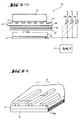
- the light coming from a light source 1 reaches a first bar system 4 via two lenses or lens systems 2 and 3, is thrown by the latter via a prism 5 onto a control element SE to be explained, which contains the control layer, and arrives from there via a concave mirror 6 to a second bar system 7 and is finally directed by a further lens or a lens system 8 onto a projection surface 9.
- the image 10 to be amplified is illuminated by a light source 11 and imaged onto the photoelectric conductor layer contained in the control element SE via a lens or a lens system 12.
- the longitudinal edges of bars 4 and 7 run perpendicular to the plane of the drawing in FIG. 1.
- the device according to the invention corresponds to the known image intensifiers. More information on their structure and function can be found in the relevant literature or e.g. the already mentioned CH-A Nos. 301 222 and 378 432 and EP-B 29 006 (- ⁇ US-A-4 519 682) can be found.
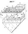
- the control element SE comprises a transparent lower carrier plate 20, on which there is a transparent conductivity coating 21 and the control layer 22 already mentioned, and a transparent upper carrier plate 23, on which in turn a metallic conductive electrode grid 25, a photoelectric conductor layer 26 and a black one , opaque and non-conductive protective layer 27 are arranged.
- the electrode grid 25 consists of a series of transparent, electrically conductive strips 25a, which are arranged in parallel at regular intervals next to one another and are aligned parallel to the longitudinal edges of the bars 4 and 7.
- the grid period of the electrode grid, designated c, is approximately 50-200 ⁇ m and is preferred as low as possible.
- the width d of the conductor strips 25a is approximately 1/6 to 1/4 of the raster period c, preferably approximately 1/5. With a practical grid period of approximately 150 ⁇ m, the strip width is then preferably approximately 30 ⁇ m and the distance between two conductor strips is accordingly approximately 120 ⁇ m.
- the individual conductor strips 25a of the electrode grid 25 are connected at their ends by a busbar 28 which is only shown schematically in the drawing and are connected to the one pole of an AC voltage source 29.
- the other pole of the voltage source 29 is connected to the conductivity coating 21 serving as counterelectrode on the lower carrier plate 20.
- the electromotive force of the voltage source 29 is approximately 200-300 V eff at a frequency of approximately 100-500 Hz, depending on the photoelectric conductor layer.
- the individual conductor strips 25a of the electrode grid 25 are therefore all at the same potential with respect to the counter electrode 21. Without exposure of the photoelectric conductor layer 26, it is insulating or poorly conductive, so that relatively flat potential troughs form between the individual conductor strips 25a, i.e. between the conductor strips there is a smaller amount of potential with respect to the counterelectrode 21 than conductor strips 25a at the location. These potential troughs lead to a wave-shaped deformation of the control layer 22, these waves being directed parallel to the longitudinal edges of the bars 4 and 7 in accordance with the orientation of the electrode grid. The light originating from the light source 1 and totally reflected on the surface 22a of the control layer 22 is deflected transversely to the bars 7 and therefore passes the bars 7 onto the projection surface 9. The latter thus appears homogeneously brightened.
- the photoelectric conductor layer 26 is illuminated homogeneously, the potentials on and between the conductor strips 25a of the electrode grid 25 are equalized and the control layer 22 does not experience any deformation. The light totally reflected by the control layer can now not pass the bars 7 onto the projection screen, and the latter remains dark.
- the control layer 22 is any elasto-viscous material, the surface or the optical properties of which can be deformed or changed by an electrical field.
- the control layer is preferably a gel layer with a thickness D of approximately 30-120 ⁇ m, preferably approximately 70 ⁇ m.
- the gel comes e.g. the quality offered under the name Sil-Gel 604 by the company Wacker, Kunststoff, Germany.
- control element SE described above according to EP-B 29 006 (- ⁇ US-A-4 519 682) still has the shortcomings explained at the outset. These deficiencies are now eliminated by the improved control elements according to the invention shown in FIGS. 3-6.
- the basic structure of these control elements according to the invention corresponds to that according to FIG. 2, so that the control elements are only shown schematically in section (parallel to the paper plane in FIG. 2). However, these sectional representations make it easy to see the details that are important for understanding the invention.
- the unchanged components of the control elements according to the invention compared to FIG. 2 are designated with the same reference numerals as in FIG. 2 and will not be explained again separately in the following.
- the most important feature of the control element SE shown in FIG. 3 is that the photoelectric conductor layer 26 is electrically insulated from the electrode grid 25 by an insulation layer 43 and that the electrically conductive strips 25a of the electrode grid alternately to one and the other pole of the AC voltage source 29 are connected, ie every second strip is at the same potential as the counter electrode 21. Furthermore, a compensating layer 44 is provided between the electrode grid 25, the strips of which are designated A and B here, and the upper carrier plate 23. This has the optical damping behavior shown in Fig. 4, the This means that the optical attenuation ⁇ of this layer is lowest in the area of the grid strips A, B of the electrode grid 25 and strongest in between. The damping is preferably effected by the reflectivity of the compensation layer. Due to the specified damping curve, the compensation layer 44 has the effect that the control light has the same control effect everywhere.
- the alternating potentials of the successive strips A, B of the electrode grid 25 have the result that the potential on the gel surface 22a is well modulated. Due to the lack of electrical contact between the electrode grid 25 and the photoelectric conductor layer 26, less undesirable space charges build up and the photoelectric conductor layer 26 remains neutral overall. Space charges in the photoelectric conductor layer tend to build up with twice the spatial frequency of the control field. As a result, the influence of the space charges in the photoelectric conductor layer on the surface 22a of the control layer 22 is much less.
- the strips A, B of the electrode grid 25 are preferably transparent, e.g. made of indium tin oxide.
- the control light can also be effective under the electrode grid, which reduces moirée phenomena.
- the insulation layer 43 is preferably made of a high-purity, high-temperature resistant plastic, e.g. Polyimide, or from an inorganic insulator, e.g. Silicon dioxide or silicon nitride.
- a high-purity, high-temperature resistant plastic e.g. Polyimide
- an inorganic insulator e.g. Silicon dioxide or silicon nitride.
- the photoelectric conductor layer 26 preferably consists of amorphous or crystalline silicon. It is advantageously interrupted by a multiplicity of non-conductive or poorly conductive tracks 26a which run transversely to the longitudinal direction of the strips A, B of the electrode grid 25 (FIG. 6). With a raster period c of 50 ⁇ m, for example, these tracks 26a are each about 1 ⁇ m wide and about 6 - 7 ⁇ m apart. The mutual distance and the number and width of the tracks 26a are dimensioned such that their presence, with uniform illumination of the photoelectric conductor layer 26, has no noticeable influence on the potential profile on the surface 22a of the control layer 22 is.
- the non-conductive or poorly conductive tracks 26a which can of course also simply be interruptions in the photoelectric conductor layer 26, prevent or complicate charge carrier transport along the strips A, B of the electrode grid 25, and thus an undesirable phenomenon similar to the so-called "spreading" of picture lines .
- the opaque protective layer 27 is non-conductive or at least has a much lower conductivity than the photoelectric conductor layer 26 without exposure to light (dark conductivity). Furthermore, it should also have no photoelectric effect. It can be realized by vapor-deposited pigments, pigments bound in epoxy resin, cermet or amorphous silicon doped with p and n.
- the air gap between the control layer 22 and the protective layer 27 is preferably with a gas with high dielectric strength, e.g. SF6 filled out.
- the control layer 26 consists of a gel and is preferably doped with additives that make the refractive index as large as possible, but without reducing the transparency.
- additives that make the refractive index as large as possible, but without reducing the transparency.
- An example of such additives is phenyl silicone oils.
- the gel layer 22 is preferably doped with additives that make the gel conductive, but without significantly impairing the optical properties.
- additives are polyacetylenes.
- the voltage source 29 advantageously supplies a square-wave voltage. As a result, the gel layer 22 experiences a uniform force as long as the conductivity of the photoelectric conductor layer 26 is low. This is favorable for the light efficiency of the bright field.
- an automatic switching device 45 is advantageously provided, which periodically swaps the polarity of the strips A and B of the electrode grid 25 (frequency 0.1 to 0.5 Hz). This will make the Gel layer 22 is not always deformed at the same point and does not undergo plastic deformation. Any remaining space charge effects that may still exist are also symmetrized.
- the strips of the same polarity are preferably electrically connected to one another at their two ends.
- a thin passivation layer 46 made of silicon dioxide or silicon nitride (FIG. 5), which suppresses disruptive surface effects on the photoelectric conductor layer 26.
- a practical exemplary embodiment of a control element SE according to FIG. 3 has the following data: Grid period c 30 ⁇ m Width of the conductor strips d 6 ⁇ m Insulation layer thickness 43 5 ⁇ m Thickness of the photoelectric conductor layer 26 0.7 ⁇ m Protective layer thickness 27 3 ⁇ m Air gap W 20 ⁇ m Thickness of the gel layer 22 40 ⁇ m
- the transparent electrodes are preferably made of indium tin oxide. All other data, unless otherwise stated, according to the prior art, for example EP-B 29 006 (- ⁇ US-A-4 519 682).
- FIG. 5 shows a further variant of a control element SE according to the invention, which essentially differs from the variant according to FIG. 3 only in that the strips of the electrode grid 25 designated A, B and C now alternate cyclically to one pole each three different AC voltage sources 29a-c are connected, the other pole of which is connected to the counter electrode 21 (ground, Reference potential). Otherwise, this variant corresponds in all details to the embodiment according to FIG. 3. Furthermore, a phase shifter stage 47 is also provided.
- the gel layer 22 can be evenly stressed at all locations averaged over time, thereby avoiding permanent deformations.
- k e.g. 1
- the temporal variation of the modulation phase ⁇ 0 takes place through the phase shifter stage 47 in such a way that ⁇ 0 periodically runs through all possible values from 0 ° to 360 ° with a frequency of 0.5 to 50 Hz, for example.
- ⁇ 0 periodically runs through all possible values from 0 ° to 360 ° with a frequency of 0.5 to 50 Hz, for example.
- "traveling waves" can be generated in the gel layer 22, which improve the resolution and average moire effects over time and thus suppress them.
- a raster period c of 20 ⁇ m with a width d of the raster strips of 5 ⁇ m has proven itself for the electrode raster 25. All other data and design features are the same as in the exemplary embodiment according to FIG. 3 or, unless specified in more detail, as in the known devices of this type.
Landscapes
- Physics & Mathematics (AREA)
- General Physics & Mathematics (AREA)
- Optics & Photonics (AREA)
- Mechanical Light Control Or Optical Switches (AREA)
- Electrochromic Elements, Electrophoresis, Or Variable Reflection Or Absorption Elements (AREA)
- Transforming Electric Information Into Light Information (AREA)
- Transforming Light Signals Into Electric Signals (AREA)
Claims (19)
- Dispositif d'amplification de l'intensité d'une image produite optiquement,dans lequel des moyens (2, 3, 6, 8) de projection projettent optiquement,par l'intermédiaire d'une surface réfléchissante (22a), au moins une zone (4) en forme de raies ou de barres, éclairée sur une surface de référence par une source lumineuse (1), sur une raie (7), formant un diaphragme non transparent à la lumière, qui lui est associée,et dans lequel la surface réfléchissante est disposée sur une couche de commande (22) susceptible d'être déformée par des forces de champ électriques et qui peut être déformée par la couche de commande ou bien est formée par la surface libre de celle-ci, comportant une couche conductrice photoélectrique (26) disposée derrière la couche de commande et parallèlement à celle-ci, sur laquelle l'image qu'il s'agit d'amplifier est projetée et qui a une influence sur le champ électrique qui agit sur la couche de commande (22), et qui règne entre un réseau (25) d'électrodes qui est placé en amont du côté éclairé de la couche conductrice photoélectrique (26) et qui comprend un très grand nombre de raies (25a) électriquement conductrices qui s'étendent les unes à côté des autres, parallèlement entre elles avec des écarts réguliers, et une contre-électrode (21) disposée en-deçà de la couche de commande (22) par rapport à la couche conductrice photoélectrique, le dispositif comportant également des moyens (6, 8) destinés à la projection de la surface réfléchissante déformée (22a), en passant devant les bords des raies, bandes ou barres formant un diaphragme (7) sur une surface de projection (9), dispositif caractérisé en ce que le réseau (25) d'électrodes est disposé de façon électriquement isolée par rapport à la couche conductrice photoélectrique (26).
- Dispositif selon la revendication 1, caractérisé en ce que la contre-électrode (21) est branchée sur l'un des pôles d'une source de tension alternative (29) et en ce que les raies électriquement conductrices (A, B) du réseau (25) d'électrodes sont alternativement raccordées à l'un et à l'autre pôle de la même source de tension alternative.
- Dispositif selon la revendication 1, caractérisé en ce que le réseau (25) d'électrodes est constitué par des premières, deuxièmes et troisièmes raies (A, B, C) qui se suivent en alternance cyclique,(appartenant au réseau (25) d'électrodes),toutes les premières, deuxièmes et troisièmes raies étant raccordées à l'un des pôles d'une première, ou d'une deuxième ou d'une troisième source (29a à 29c) de tension alternative, et en ce que l'autre pôle des trois sources de tension alternative,est raccordé à la contreélectrode (21).
- Dispositif selon une des revendications 1 à 3, caractérisé en ce que le réseau (25) d'électrodes est, optiquement, sensiblement transparent et est, de préférence, constitué par de l'oxyde d'indium-étain.
- Dispositif selon une des revendications 1 à 4, caractérisé en ce que, sur le côté du réseau (25) d'électrodes opposé à la contre-électrode (21), est disposée une couche (44) de compensation qui atténue moins la lumière dans la zone des raies (A à C) du réseau d'électrodes et qui l'atténue davantage entre les raies.
- Dispositif selon la revendication 5, caractérisé en ce que la couche (44) de compensation présente une capacité de réflexion localement différente, qui provoque une atténuation localement différente de lumière.
- Dispositif selon une des revendications 1 à 6, caractérisé en ce que le réseau d'électrodes est isolé électriquement au moyen d'une couche (43) d'isolation, réalisée en une matière plastique très pure et résistante à la chaleur, par exemple en polyimide, ou en un matériau minéral tel que le dioxyde de silicium ou le nitrure de silicium.
- Dispositif selon une des revendications 1 à 7, caractérisé en ce que la couche conductrice photoélectrique (26) est constituée par du silicium amorphe ou cristallin.
- Dispositif selon une des revendications 1 à 8, caractérisé en ce que la couche conductrice photoélectrique (26) est interrompue par un grand nombre de pistes (26a) relativement étroites non conductrices ou mauvaises conductrices de l'électricité, qui s'étendent perpendiculairement aux raies électriquement conductrices (A, B) du réseau (25) d'électrodes et qui rendent difficile ou empêchent le transport de supports de charge le long des raies (A, B).
- Dispositif selon des revendications 1 à 9, caractérisé en ce qu'en amont de la couche conductrice photoélectrique (26) est disposée, du côté de la couche de commande, une couche noire (27) sensiblement non transparente, dont la conductibilité électrique est sensiblement plus faible que la conductibilité,dans l'obscurité,de la couche conductrice photoélectrique (26) et qui ne présente aucun effet de photoélectricité.
- Dispositif selon une des revendications 1 à 10, caractérisé en ce qu'entre la couche de commande (22) et la couche conductrice photoélectrique (26), ou la couche noire (27), il y a un espace intermédiaire rempli d'un gaz doté d'une grande résistance au claquage.
- Dispositif selon une des revendications 1 à 11, caractérisé en ce que la couche de commande (22) est constituée par un gel dopé au moyen d'additifs qui donnent à l'indice de réfraction de la couche de commande une valeur aussi grande que possible, sans toutefois réduire sa transparence.
- Dispositif selon une des revendications 1 à 12, caractérisé en ce que la couche de commande (22) est constituée par un gel dopé au moyen d'additifs qui rendent le gel conducteur, sans sensiblement exercer d'influence négative sur ses propriétés optiques.
- Dispositif selon une des revendications 1 à 13, caractérisé en ce que la source de tension alternative (29) délivre une tension rectangulaire ou crénelée.
- Dispositif selon une des revendications 1 à 14, caractérisé en ce que des moyens (45) sont prévus pour raccorder, en alternance périodique, les raies (A, B) du réseau (25) d'électrodes à l'un ou à l'autre des pôles de la source de tension alternative (29).
- Dispositif selon une des revendications 1 à 15, caractérisé en ce que les raies (A à c) du réseau (25) d'électrodes, qui sont dans chaque cas au même potentiel, sont chacune raccordées ensemble de façon électriquement conductrice à leurs deux extrémités.
- Dispositif selon une des revendications 1 à 16,, caractérisé en ce que la couche conductrice photoélectrique (26) reçoit,immédiatement en amont ou en aval, une couche (46) relativement mince de passivation qui est par exemple en dioxyde de silicium ou en nitrure de silicium, et qui réduit fortement les effets de surface perturbateurs pouvant s'exercer sur la couche conductrice photoélectrique (26).
- Dispositif selon une des revendications 3 à 17, caractérisé en ce que les trois sources de tension alternatives (29 à 29c) délivrent des tensions alternatives égales modulées en amplitude, mais présentant un décalage de phase, de préférence de 120°, de chacune d'elles par rapport aux autres.
- Dispositif selon la revendication 18, caractérisé en ce qu'il comporte la présence de moyens (47) pour faire varier dans le temps les phases(φ₀)de la modulation d'amplitude des tensions alternatives.
Applications Claiming Priority (2)
| Application Number | Priority Date | Filing Date | Title |
|---|---|---|---|
| CH2208/86 | 1986-05-30 | ||
| CH220886 | 1986-05-30 |
Related Child Applications (1)
| Application Number | Title | Priority Date | Filing Date |
|---|---|---|---|
| EP91100344.0 Division-Into | 1991-01-12 |
Publications (2)
| Publication Number | Publication Date |
|---|---|
| EP0247972A1 EP0247972A1 (fr) | 1987-12-02 |
| EP0247972B1 true EP0247972B1 (fr) | 1992-01-15 |
Family
ID=4228414
Family Applications (2)
| Application Number | Title | Priority Date | Filing Date |
|---|---|---|---|
| EP91100344A Expired - Lifetime EP0428501B1 (fr) | 1986-05-30 | 1987-05-25 | Amplificateur d'images optiques |
| EP87810313A Expired - Lifetime EP0247972B1 (fr) | 1986-05-30 | 1987-05-25 | Amplificateur d'images optiques |
Family Applications Before (1)
| Application Number | Title | Priority Date | Filing Date |
|---|---|---|---|
| EP91100344A Expired - Lifetime EP0428501B1 (fr) | 1986-05-30 | 1987-05-25 | Amplificateur d'images optiques |
Country Status (4)
| Country | Link |
|---|---|
| US (1) | US4779963A (fr) |
| EP (2) | EP0428501B1 (fr) |
| JP (1) | JPS6324226A (fr) |
| DE (2) | DE3787979D1 (fr) |
Families Citing this family (3)
| Publication number | Priority date | Publication date | Assignee | Title |
|---|---|---|---|---|
| US4909611A (en) * | 1988-04-21 | 1990-03-20 | Systems And Simulation, Inc. | Large active screen display |
| DE4125952C2 (de) * | 1991-08-06 | 1993-10-14 | Dornier Gmbh | Optischer Leistungsbegrenzer |
| US5521746A (en) * | 1993-02-22 | 1996-05-28 | Engle; Craig D. | Poppet valve modulator |
Family Cites Families (9)
| Publication number | Priority date | Publication date | Assignee | Title |
|---|---|---|---|---|
| CH301222A (de) * | 1952-04-16 | 1954-08-31 | Foerderung Forschung Gmbh | Anordnung zur Verstärkung der Lichtintensität eines optisch projizierten Bildes. |
| CH378432A (de) * | 1960-06-30 | 1964-06-15 | Foerderung Forschung Gmbh | Einrichtung zur Verstärkung der Intensität eines optisch erzeugten Bildes |
| US3465202A (en) * | 1965-10-25 | 1969-09-02 | Matsushita Electric Industrial Co Ltd | Electroluminescent device for deriving a bright output image from a dark input image |
| CH454296A (de) * | 1967-03-17 | 1968-04-15 | Foerderung Forschung Gmbh | Einrichtung zur Verstärkung der Intensität eines optisch erzeugten Bildes |
| US3638027A (en) * | 1970-03-11 | 1972-01-25 | Philips Corp | Image display device comprising an auxiliary light source |
| US4023969A (en) * | 1975-01-03 | 1977-05-17 | Xerox Corporation | Deformable elastomer imaging member employing an internal opaque deformable metallic layer |
| JPS5518151A (en) * | 1978-07-26 | 1980-02-08 | Canon Inc | Input device of photo electric conversion information |
| US4280756A (en) * | 1979-01-02 | 1981-07-28 | Itek Corporation | Piezoelectric bi-morph mirror actuator |
| EP0029006B1 (fr) * | 1979-11-08 | 1983-04-13 | GRETAG Aktiengesellschaft | Amplificateur d'image optique |
-
1987
- 1987-05-20 US US07/051,639 patent/US4779963A/en not_active Expired - Fee Related
- 1987-05-25 EP EP91100344A patent/EP0428501B1/fr not_active Expired - Lifetime
- 1987-05-25 DE DE91100344T patent/DE3787979D1/de not_active Expired - Fee Related
- 1987-05-25 DE DE8787810313T patent/DE3775990D1/de not_active Expired - Fee Related
- 1987-05-25 EP EP87810313A patent/EP0247972B1/fr not_active Expired - Lifetime
- 1987-05-29 JP JP62131944A patent/JPS6324226A/ja active Pending
Also Published As
| Publication number | Publication date |
|---|---|
| EP0247972A1 (fr) | 1987-12-02 |
| DE3787979D1 (de) | 1993-12-02 |
| DE3775990D1 (de) | 1992-02-27 |
| EP0428501A1 (fr) | 1991-05-22 |
| JPS6324226A (ja) | 1988-02-01 |
| US4779963A (en) | 1988-10-25 |
| EP0428501B1 (fr) | 1993-10-27 |
Similar Documents
| Publication | Publication Date | Title |
|---|---|---|
| DE3586587T2 (de) | Elektrodenstrukturen fuer eine elektrophoretische vorrichtung. | |
| DE69111906T2 (de) | Verfahren zur Herstellung von Matrixen von MIM-Anordnungen und solche Matrixen enthaltende Anzeigevorrichtungen. | |
| DE69333323T2 (de) | Flüssigkristall-Anzeigevorrichtung | |
| DE69627066T2 (de) | Flüssigkristallanzeigeeinrichtung mit aktiver Matrix mit an einem unabhängigen Potential angeschlossener Lichtschutzelektrode | |
| DE1002479C2 (de) | Strahlendetektor und -verstaerker, insbesondere elektronisches Verteilungssystem | |
| DE2635891A1 (de) | Fluessigkristallzelle | |
| DE3880046T2 (de) | Elektronenstrahl angesteuertes fluessigkristallichtventil mit flaechenkaftem eingabeleiter. | |
| DE2163314B2 (de) | Anzeigevorrichtung mit einer Flüssigkristallschicht | |
| DE1564223A1 (de) | Elektrooptische Anordnung zur Lichtsteuerung | |
| DE69125790T2 (de) | Optische Vorrichtung vom Wellenleitertyp | |
| EP0247972B1 (fr) | Amplificateur d'images optiques | |
| DE69533187T2 (de) | Elektrooptische Anzeigevorrichtung | |
| DE69533613T2 (de) | Optische Ablenkungsvorrichtung mit kontinuierlicher Steuerung des Ablenkungswinkels | |
| DE69010255T2 (de) | Elektrolumineszenzanzeigebildschirm mit Speicher und mit besonderer Elektrodenkonfiguration. | |
| EP0029006B1 (fr) | Amplificateur d'image optique | |
| DE69511527T2 (de) | Plasmaadressierbare flüssigkristallanzeigevorrichtung mit reduzierten spaltenspannungen | |
| DE3214584C2 (de) | Elektrooptische Vorrichtung | |
| DE3434388C2 (fr) | ||
| DE3148427A1 (de) | Ortsabhaengig modulierbarer interferenzfilter | |
| DE3788639T2 (de) | Verfahren und vorrichtung zur lichtablenkung. | |
| DE69118768T2 (de) | Optische Vorrichtung | |
| EP0329839B1 (fr) | Dispositif de restitution d'image plat | |
| DE3642321A1 (de) | Projektionsroehre | |
| DE102017211502B4 (de) | Polarisationseinheit mit einer schaltbaren Polarisationsfilterstruktur, Polarisator und Verwendung einer Polarisationseinheit oder eines Polarisators | |
| DE2809997A1 (de) | Elektrodenanordnung |
Legal Events
| Date | Code | Title | Description |
|---|---|---|---|
| PUAI | Public reference made under article 153(3) epc to a published international application that has entered the european phase |
Free format text: ORIGINAL CODE: 0009012 |
|
| 17P | Request for examination filed |
Effective date: 19870527 |
|
| AK | Designated contracting states |
Kind code of ref document: A1 Designated state(s): CH DE FR GB LI NL SE |
|
| 17Q | First examination report despatched |
Effective date: 19900619 |
|
| GRAA | (expected) grant |
Free format text: ORIGINAL CODE: 0009210 |
|
| AK | Designated contracting states |
Kind code of ref document: B1 Designated state(s): CH DE FR GB LI NL SE |
|
| XX | Miscellaneous (additional remarks) |
Free format text: TEILANMELDUNG 91100344.0 EINGEREICHT AM 25/05/87. |
|
| ET | Fr: translation filed | ||
| REF | Corresponds to: |
Ref document number: 3775990 Country of ref document: DE Date of ref document: 19920227 |
|
| GBT | Gb: translation of ep patent filed (gb section 77(6)(a)/1977) | ||
| PLBE | No opposition filed within time limit |
Free format text: ORIGINAL CODE: 0009261 |
|
| STAA | Information on the status of an ep patent application or granted ep patent |
Free format text: STATUS: NO OPPOSITION FILED WITHIN TIME LIMIT |
|
| 26N | No opposition filed | ||
| PGFP | Annual fee paid to national office [announced via postgrant information from national office to epo] |
Ref country code: SE Payment date: 19930330 Year of fee payment: 7 |
|
| PG25 | Lapsed in a contracting state [announced via postgrant information from national office to epo] |
Ref country code: SE Effective date: 19940526 |
|
| PGFP | Annual fee paid to national office [announced via postgrant information from national office to epo] |
Ref country code: NL Payment date: 19940531 Year of fee payment: 8 |
|
| PGFP | Annual fee paid to national office [announced via postgrant information from national office to epo] |
Ref country code: CH Payment date: 19940819 Year of fee payment: 8 |
|
| EUG | Se: european patent has lapsed |
Ref document number: 87810313.4 Effective date: 19941210 |
|
| EUG | Se: european patent has lapsed |
Ref document number: 87810313.4 |
|
| PGFP | Annual fee paid to national office [announced via postgrant information from national office to epo] |
Ref country code: FR Payment date: 19950407 Year of fee payment: 9 |
|
| PGFP | Annual fee paid to national office [announced via postgrant information from national office to epo] |
Ref country code: DE Payment date: 19950424 Year of fee payment: 9 |
|
| PGFP | Annual fee paid to national office [announced via postgrant information from national office to epo] |
Ref country code: GB Payment date: 19950427 Year of fee payment: 9 |
|
| PG25 | Lapsed in a contracting state [announced via postgrant information from national office to epo] |
Ref country code: LI Effective date: 19950531 Ref country code: CH Effective date: 19950531 |
|
| PG25 | Lapsed in a contracting state [announced via postgrant information from national office to epo] |
Ref country code: NL Effective date: 19951201 |
|
| REG | Reference to a national code |
Ref country code: CH Ref legal event code: PL |
|
| NLV4 | Nl: lapsed or anulled due to non-payment of the annual fee |
Effective date: 19951201 |
|
| PG25 | Lapsed in a contracting state [announced via postgrant information from national office to epo] |
Ref country code: GB Effective date: 19960525 |
|
| GBPC | Gb: european patent ceased through non-payment of renewal fee |
Effective date: 19960525 |
|
| PG25 | Lapsed in a contracting state [announced via postgrant information from national office to epo] |
Ref country code: FR Effective date: 19970131 |
|
| PG25 | Lapsed in a contracting state [announced via postgrant information from national office to epo] |
Ref country code: DE Effective date: 19970301 |
|
| REG | Reference to a national code |
Ref country code: FR Ref legal event code: ST |