EP0247141B1 - Systeme de controle et de reparation de plaquettes de circuits imprimes - Google Patents
Systeme de controle et de reparation de plaquettes de circuits imprimes Download PDFInfo
- Publication number
- EP0247141B1 EP0247141B1 EP86907057A EP86907057A EP0247141B1 EP 0247141 B1 EP0247141 B1 EP 0247141B1 EP 86907057 A EP86907057 A EP 86907057A EP 86907057 A EP86907057 A EP 86907057A EP 0247141 B1 EP0247141 B1 EP 0247141B1
- Authority
- EP
- European Patent Office
- Prior art keywords
- pcb
- test
- pcbs
- stations
- transport
- Prior art date
- Legal status (The legal status is an assumption and is not a legal conclusion. Google has not performed a legal analysis and makes no representation as to the accuracy of the status listed.)
- Expired - Lifetime
Links
Images


Classifications
-
- G—PHYSICS
- G01—MEASURING; TESTING
- G01R—MEASURING ELECTRIC VARIABLES; MEASURING MAGNETIC VARIABLES
- G01R31/00—Arrangements for testing electric properties; Arrangements for locating electric faults; Arrangements for electrical testing characterised by what is being tested not provided for elsewhere
- G01R31/28—Testing of electronic circuits, e.g. by signal tracer
- G01R31/2801—Testing of printed circuits, backplanes, motherboards, hybrid circuits or carriers for multichip packages [MCP]
- G01R31/2806—Apparatus therefor, e.g. test stations, drivers, analysers, conveyors
- G01R31/2808—Holding, conveying or contacting devices, e.g. test adapters, edge connectors, extender boards
-
- G—PHYSICS
- G01—MEASURING; TESTING
- G01R—MEASURING ELECTRIC VARIABLES; MEASURING MAGNETIC VARIABLES
- G01R31/00—Arrangements for testing electric properties; Arrangements for locating electric faults; Arrangements for electrical testing characterised by what is being tested not provided for elsewhere
- G01R31/28—Testing of electronic circuits, e.g. by signal tracer
- G01R31/2801—Testing of printed circuits, backplanes, motherboards, hybrid circuits or carriers for multichip packages [MCP]
- G01R31/2806—Apparatus therefor, e.g. test stations, drivers, analysers, conveyors
-
- H—ELECTRICITY
- H05—ELECTRIC TECHNIQUES NOT OTHERWISE PROVIDED FOR
- H05K—PRINTED CIRCUITS; CASINGS OR CONSTRUCTIONAL DETAILS OF ELECTRIC APPARATUS; MANUFACTURE OF ASSEMBLAGES OF ELECTRICAL COMPONENTS
- H05K2203/00—Indexing scheme relating to apparatus or processes for manufacturing printed circuits covered by H05K3/00
- H05K2203/01—Tools for processing; Objects used during processing
- H05K2203/0147—Carriers and holders
- H05K2203/0165—Holder for holding a Printed Circuit Board [PCB] during processing, e.g. during screen printing
Definitions
- This invention in general relates to a method and apparatus for testing and/or repairing printed circuit boards (PCBs), and in particular it relates to an automated multi-station system capable of testing and/or repairing PCBs of different types, concurrently, including: an input station for entering PCBs into said system; a plurality of test and/or repair stations; a transport system interconnecting all of said stations for transporting PCBs between said stations; and control means for supervising transport of said PCBs by said transport system, operation of said input station and activation of said test and/or repair stations.
- PCBs printed circuit boards
- the invention also relates to a method for automating test and/or repair operations to be performed on PCBs in a multi-station system so that such operations can be preformed by the system on PCBs of different types concurrently, wherein PCBs are transported between stations of the system by an interconnecting transport system under the control of a control unit.
- printed circuit board refers generically to electrical circuits which are constructed on or within supporting strata. The use of this term is not intended to limit this invention to electrical circuits having conductive members formed by "printing” techniques nor to circuits formed on or within a supporting stratum of any specific construction.
- PCBs printed circuit boards
- this electrical connection is accomplished with a fixture assembly upon which the PCB is positioned.
- the fixture assembly incorporates a plurality of conductive probes (traditionally referred to as a bed of nails) which are selectively positioned therein to correspond to predetermined electrical nodes on the PCB. After the PCB is positioned upon the fixture assembly the probes are biased into electrical contact with such nodes.
- the various probes of the fixture assembly are in turn electrically connected to stimulus and measurement means within the test system which stimulate the nodes and which measure the responses which occur at the nodes of the PCB under test as a result of such stimulus.
- a separate fixture assembly is generally required for each different PCB to be tested due to the variation of the circuits of the PCB and of the electrical nodes located therein. Since the electrical connection between the electrical nodes of the PCB and the test system is very critical, since the trend is to design PCBs with electrical nodes which are very densely packed, and since there is such a variation in the size and configuration of the different PCBs, the accurate loading or positioning of a PCB with respect to the fixture assembly and the accurate loading and positioning of the fixture assembly as well as the electrical connection of the fixture assembly to the stimulus and measurement means of the test system have typically been manual processes which make up an excessively large proportion of the total test time.
- US-A-4,348,276 describes an automatic testing apparatus for automatically testing, adjusting and sorting PCBs of a single specific type, at any one time, in a predefined, fixed sequence determined by the physical arrangement of test stations along an one-way conveyor system.
- PCBs are introduced into the apparatus through a casing and placed onto a pallet.
- the pallet passes first into a parts testing device, where the components of the PCB are tested, then into each of two parts measuring/adjustment devices. If any failures are found, the PCB is transferred to an unfit parts conveyor. Consequently, this known testing apparatus is specific to a single given product type at any given time and limited to a particular, fixed process sequence at all times. It does not represent a flexible automation system capable of processing PCBs of different types concurrently and does also not include a provision for repair of PCBs within the system. The failed PCBs requiring repair simply disappear.
- the problem to be solved by the invention is to provide a flexible automation system capable of processing PCBs of different types concurrently and including provisions for repair of PCBs within the system, the apparatus having flexibility in routing PCBs between different stations of the system and capability for controlling such transport in accordance with a predetermined process sequence file for each type of PCB entered into the system to accomodate the test and/or repair of PCBs of different types concurrently.
- the present invention proposes an apparatus and a method for testing and/or repairing PCBs which substantially minimizes the aforementioned limitations and which can be used to automatically select, transport, and load the fixture assembly or comparable circuit means required to test or repair a given PCB; transport and position the PCB to be tested or repaired with respect to the circuit means; electrically connect the same to the circuitry adapted to selectively test the electrical circuits of the PCB; test the PCB by stimulating various nodes within the circuits of the PCB with a predetermined signal and measuring the response of the electrical circuit to the signal; determine in view of an interpretation of the test results whether the PCB being tested is acceptable, defective, or requires additional testing or repair; conduct the additional tests or remove the PCB from the circuit means and transport the PCB to another area within the test or repair system corresponding to the determined status of the PCB; determine whether there are other PCBs to be tested or repaired which will utilize the same circuit means presently loaded within the test system, and if so, sequentially transport and position one of such PCBs with respect to the circuit means
- the system according to the present invention is not strictly limited to testing PCBs.
- stages can be advantageously included within the system to manufacture or repair PCBs, e.g. to insert or remove parts, to make adjustments to parts, to solder or unsolder parts, to burn in parts, etc.
- this disclosure utilizes the terminology "test and/or repair” to generically refer to such operations.
- test and/or repair For the sake of brevity and readability such alternative language has not, however, been repeated in each and every instance. The failure, therefore, to specifically refer to both terms should not be viewed as intentionally limiting the reference, for example, to strictly test operations.
- the testing and/or repair of a PCB may require multiple stages and, therefore, the movement of the PCB from one stage to another.
- Conveyor means are provided to efficiently and accurately load a PCB, for example, onto a selected test stage prior to the test and for removing the PCB from the test stage after the test.
- the system further includes control means to efficiently route the PCB through the various stages required to test and/or repair a given PCB.
- the present invention further includes mounting the PCB within a carrier which is adapted to uniquely position and restrain the PCB therein.
- the carriers are adjustable to accommodate various shapes and sizes of PCBs and are adapted to facilitate the movement of the PCBs into and out of the various test stages of the test system by the automated conveyor means.
- the carriers include structure which in cooperation with other components of the test system facilitate the precise positioning of the PCB with respect to the circuit means.
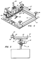
- FIG. 1 A perspective view illustrating various functional modules of the test system 10 according to the present invention is provided in Figure 1.
- the system 10 can include such multiple test stages, for example, stages 11a and 11b.
- the test stages 11 can be identical, or they can be of different types, e.g. functional, in-circuit, combinational, special device or component testers, bare board testers, etc.
- Figure 1 illustrates two test stages 11, the present invention is not intended to be limited to this number nor to the descriptions provided above.
- Conveyor means are provided to load and unload such PCBs from the test and/or repair stages and to transport the PCBs there between.
- the conveyor means of the present invention are specifically adapted to afford flexibility in the configuration of the test system 10.
- Conveyor 12 is a linear conveyor which moves the PCB in two directions, i.e., towards as well as away from a stage. It should be noted that such forwards and backwards motion is net commonly found in typical automated production lines which generally transport the items under process in one common direction. A more complex motion is however required to afford conveyor 12 to be utilized to transport a PCB both into as well as out of a test stage 11, as is included in the present invention.
- conveyor 13 incorporates the capability for the rotational movement of the PCB in addition to linear movement.
- Various combinations of conveyors 12 and 13 can be utilized to facilitate multiple arrangements of test stages 11 in order to optimize the test system 10 to the particular user requirements. Utilizing different types of conveyors 12 and 13 not only provides increased efficiency, but additionally allows a user to reduce the cost of the test system by utilizing the less expensive linear conveyor 12 for those applications when rotational movement is not required: It also allows the user to easily alter the configuration of the test system 10 as the requirements change.
- FIG. 1 illustrates a repair station 15, such as a model 404 repair station which is commercially available from the FACTRON/Schlumberger division of Fairchild Camera and Instrument Corporation.
- This repair station 15 incorporates a repair and adjustment capability as well as a testing capability.
- a PCB can be diverted to stage 15 when repair (e.g. desoldering and replacement of components) or adjustments (e.g. repositioning of knobs or switches within the PCB) are required prior to completing the testing of the PCB.
- manual probing of the PCB may be accomplished such as may be required, for example, to trace a fault indicated as being on a common node having multiple connections thereto.
- Buffering or set-up stages 16 are also included to afford a smooth flow in and out of the various test or repair stages.
- the buffering stages 16 can also be utilized as input and output stages for the test system 10.
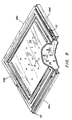
- the present invention utilizes a carrier 20, which is best illustrated in Figure 2.
- the carrier 20 is designed to be adjustable to accommodate a wide range of sizes and configurations of PCBs 19.
- the test system 10 can accommodate various sizes and configurations of PCBs without requiring manual intervention or downtime to adjust the remainder of the test system 10 for a specific size or configuration PCB.
- the test system 10 of the present invention can concurrently accommodate or intermix different PCBs 19, e.g. different shapes and sizes. This is particularly useful and cost effective for users who do not consistently test a large volume of the same PCBs 19.
- the carrier 20 includes a frame having interconnected members 22 circumscribing and thereby defining an interior area sufficiently large to accommodate the PCBs 19 which are intended to be tested. At least two of the interconnected members 22a and 22c are generally parallel to each other and form opposing supports for two suspension beams 23. The suspension beams 23 are mounted in a manner which facilitates the lateral adjustment of the suspension beams 23 along the members 22a and 22c (See Fig. 3).
- the interior surface of each of the members 22a and 22c has a longitudinal channel 24 therein which is adapted to loosely receive the distal ends of the suspension beams 23. Such distal ends include a threaded bore having a corresponding set screw 25 engaged therein.
- Loosening such set screw 25 affords the movement of the suspension beams 23 within the channels 24.
- the beams 23 can thus be displaced with respect to each other to accommodate varying lengths (or widths) of the PCB.
- One or more support brackets 26 are adjustably mounted on each of the beams 23 and adapted to engage the edges of a PCB 19. The brackets 26 (see Fig.
- brackets 26 which can be biased toward the beams 23 to frictionally engage the beams 23 but which can also be pivoted to a position spaced from the beams 23 to release the brackets 26 from frictional engagement with the beams 23 and afford the movement of the brackets 26 along the beams 23 in order to adjust for differing sizes and shapes of PCBs.
- the edge of the brackets 26 which is proximate to the PCB 19 has a groove 28 therein which is adapted to receive an edge of the PCB 19.
- the proximate end 31 of the spring 30 is also adapted to receive this edge of the PCB 19.
- the bracket 26 is designed such that the absence of a PCB 19 will allow the spring 30 to pivot toward its spaced position thereby releasing the beam 23.
- the parallel side members 22a and 22c also facilitate the transport of the carrier 20 by the conveyors 12 and 13.
- at least one surface 21 of the generally parallel side members 22a and 22c of the carrier 20 is substantially planar and has a coefficient of friction promoting the transport of the carrier 20 by the conveyors 12 or 13.
- each of the carriers 20 also contain structure to accurately locate the carriers 20 when they are positioned within any of the various stages 11 or 15 making up the system 10, as will be explained.
- the location holes 27 provide this locating structure.
- the conveyors 12 and 13 provide for the transport of the carriers 20 and the PCBs therein between the various stages 11 and 15 of the test system 10.
- the illustrated embodiment (See Fig. 5) employs driven rollers 32 which establish frictional contact with the planar surface on the members 22a and 22c of the carriers 20.
- the rollers 32 are driven in a conventional manner by a dc motor 34.
- the driven rollers 32 are supported on chassis 31 in a conventional manner and positioned adjacent both the opposing ends of the conveyors 12 or 13 to maintain control over a transported carrier 20 as it passes in either direction into or out of one conveyor 12 or 13 to an adjacent conveyor 12 or 13, or into and out of a test stage 11 or a repair stage 15, as is applicable.
- the direction of travel of the rollers 32 is determined by the polarity of the dc motor 34.
- Guide rails 91 also supported upon the chassis 31 in a conventional manner and located adjacent opposing sides of the path of the carrier 20 contain channels 92 which are adapted to receive the projecting ridges 29 of the carriers 20 thereby guiding as well as supporting the carriers 20.
- the conveyor 13 includes a stepper motor 95 and associated conventional bearing and gearing mechanisms or their equivalent (not shown), to rotate the chassis 31 supporting the rollers 32.
- the dc motor 34 and therefore the driven rollers 32, as well as the stepper motor 95 are microprocessor controlled to afford flexibility in the path along which, and the speed at which a given carrier 20 is transported, as well as accurate control of the movement of the carrier 20 or whatever other components are being transported.
- Conveyor 12 and conveyor 13 are substantially identical except that conveyor 12 excludes the stepper motor 95 and its associated mechanisms.
- Each of the conveyors 12 and 13 also includes appropriate sensors (See Fig. 14) to determine the presence and location of a carrier 20 or other transported component therein.
- sensors also determine the relative positioning of the chassis 31 of the rotable conveyor 13. This can be accomplished with mechanical, optical, magnetic, capacitive, or other type of conventional sensors. If the test system 10 requires a conveyor to stop or hold the transport of a carrier 20 or other transported component, stop solenoids are also provided at the entrance and exit ends of such conveyors. When actuated the moveable element of such solenoids is interposed within the path of the carriers 20 to prevent further motion.
- the conveyors 12 and 13 are adapted to be utilized in modular form. For example, one of the conveyors 13 can contain a conveyor controller or microprocessor (See Figure 14) which can provide control for some predetermined quantity of slave conveyors 12.
- slave conveyors 12 can simply be plugged into the master conveyor controller and such controller can be programmed with the location and identity of the additional conveyors 12 and 13 being utilized within the test system 10 and plugged therein, thereby avoiding the need for redundant microprocessors within each of the slave conveyors 12.
- Each slave conveyor will, however, contain drivers, sensors, and stops to the extent required, such as have been described above.
- the conveyor means also includes an automation interface 38 (See Fig. 6) which interfaces the test and repair stages 11 and 15 with the conveyors 12 or 13.
- the automation interface 38 of the present invention is adapted to be utilized with existing testers such as are now commercially available.
- the automation interface 38 contains driven rollers 39 similar to those utilized by the conveyors 12 and 13.
- the driven rollers 39 are positioned to engage the parallel side members 22a and 22b (See Fig. 7) of the carriers 20 as the carriers 20 exit from the conveyors 12 or 13. In this manner the rollers 39 can maintain control of the carriers 20 when the rollers 32 of the conveyors 12 or 13 have lost effective control.
- the driven rollers 39 are driven by dc motor 96, which is also under microprocessor control.
- DC motor 96 is mounted upon a supporting column 97 by a bracket 98.
- the supporting column 97 is in turn rotatably mounted upon a bracket assembly 99 which is affixed to the frame 100 of the automation interface 38.
- a solenoid 101 or similar device which can be actuated to extend an arm 102 to the position indicated by 102a (as shown by dashed lines).
- the arm 102 is pivotably connected to the supporting column 97. Therefore, the extension of the arm 102 will rotate the column 97.
- Such rotation of the column 97 will pivot the dc motor 96 to a position 96a where the driven rollers 39 pass through an opening within the rails 44 and frictionally engage the carriers 20.
- the automation interface 38 further contains elevator means 40 (See Fig. 8) upon which the driven rollers 39 are mounted and which is adapted to raise and/or lower the carriers 20 with respect to the operating level of the conveyors 12 or 13.
- the elevator means 40 comprise two spaced rails 44 which are substantially parallel to each other.
- Each of the rails 44 contains a longitudinal channel 45 therein which is adapted to receive and support the projecting ridge 29 extending along the side members 22a and 22c of the carriers 20.
- the rails 44 are themselves supported on air cylinders 43 or the like which afford the relative movement of the rails 44 from a position supporting the carriers 20 to a position where the rails 44 are spaced from the carriers 20.
- the air cylinders 43 are in turn supported by the shuttle members 42 of lead screw mechanisms 41, and the lead screw mechanisms 41 are driven by a stepper motor 36 which is microprocessor controlled.
- a drive belt 35 in combination with various pulleys are driven by motor 36 and in turn drive lead screw mechanisms 41 located at each of the opposing corners of the rails 44. Rotation of the multiple lead screw mechanisms 41 by the motor 36 will raise or lower the rails 44 in a controllable manner.
- the rails 44 can therefore be positioned at the operating level of the conveyors 12 and 13, and the air cylinders 43 can be actuated to move the rails 44 to the position at which they can support the carriers 20.
- solenoid 101 can be actuated to bring the driven rollers 39 into frictional engagement with the carrier 20.
- a carrier 20 can then be transported by the driven rollers 32 of the conveyors 12 or 13 and/or the driven rollers 39 of the automation interface 38 into the channels 45 of the rails 44.
- Conventional mechanical stops or solenoids (See Fig. 14) can be utilized to ensure the carrier 20 is fully transported and accurately positioned within the rails 44.
- the solenoid 101 can then retract the driven rollers 39 and the lead screw mechanisms 41 can be driven to raise or lower the carrier 20 from the operating level of the conveyor 12 or 13 to the operating level of the repair or test stage 11 or 15.
- the automation interface also includes appropriate sensors (See Fig.14) similar to those described with regard to the conveyors to determine the presence of a carrier 20 or other transported article therein. Similarly, sensors are also available to determine the positioning of the elevator means 40 and the rails 44.
- the fixture assemblies 47 include a frame having interconnected members 48a-48b circumscribing and thereby defining an interior area sufficiently large to accommodate the larger PCBs which are intended to be tested.
- the frame 48 has at least 2 parallel side members 48a and 48c adapted to afford the transport of the fixture assembly 47 by the conveyers 12 and 13.
- at least one surface on each of the parallel side members 48a and 48c of the fixture assembly 47 is substantially planar and has a coefficient of friction which will promote the transport of the fixture assembly 47 by the conveyor means 12 or 13.
- Side members 48a and 48c also include a projecting ridge 58 which will be received by the aforementioned channels 45 and 92 of the conveyor means.
- location holes 52 similar to those described within the carrier 20 are also added to facilitate locating the fixture assembly 47 with respect to the automation interface 38.
- Supported within the frame 48 is a non-conductive plate 49.
- this plate 49 is manufactured from materials having characteristics resulting in a plate 49 which is both lightweight and yet capable of withstanding substantial forces without significant deformation.
- One such material is manufactured and sold by General Electric Company under the designation G-10 epoxy glass cloth, although comparable glass, paper or cloth laminates are also useable.
- a predetermined array of electrical probes 51 are supported within and pass through this plate 49. These probes 51 are positioned in a pre-arranged pattern to correspond with selected nodes on the PCB 19 which is to be tested.
- the array of probes 51 is electrically connected to an array of posts 53 which are supported within a contact panel plate 54. Either individual wiring or a personality or universal matrix platen concept such as is described in the 061 Patent could be utilized to provide this electrical connection.
- the contact panel plate 54 is also constructed from materials similar to those described with respect to plate 49, and is similarly affixed to the frame 48. Spacers 55 between plate 54 and plate 49 ensure that plates 54 and 49 remain substantially parallel and rigid.
- the test stages 11 and 15 contain a receiver 56 also having an array of probes 57 which correspond to the array of posts 53.
- the probes 57 of the receiver 56 are electrically connected to the various stimulus and measurement means included within the test stages 11 and 15.
- Actuating means such as the vacuum described in the 061 Patent are utilized to draw the posts 53 of the contact panel 54 toward the probes 57 of the receiver 56 thereby establishing electrical connection between the probes 57 of the receiver 56 and the posts 53 of the fixture assembly 47.
- Alternative actuating means such as electronic motors, hydraulic cylinders, lever mechanisms, camming mechanisms, etc. can also be utilized to establish this electrical connection.
- the fixture assemblies 47 can be transported by the conveyors 12 and 13 to a desired automation interface 38 of the required stage 11 or 15.
- the elevator means 40 of the automation interface 38 can be used to raise or lower the fixture assembly 47 from the operating level of the conveyors 12 and 13 to a level where the contact panel plate 54 can be brought into preliminary engagement with the receiver 56.
- the air cylinders 43 supporting the rails 44 can be actuated to cause the rails 44 to release the projecting side members 49 of the fixture assemblies 47.
- the exact positioning of the fixture assemblies 47 with respect to the stages 11 and 15 is achieved by including guide columns 60 within the test stages 11 and 15. These guide columns 60 cooperate with the location of the location holes 52 within the fixture assembly 47 to accurately position the fixture assemblies 47.
- the columns 60 or the holes 52 are tapered to ensure engagement.
- a PCB 19, positioned within a carrier 20, can then be transported to the test stage in a manner already described and positioned upon the fixture assembly 47.
- the test systems' actuating means e.g. a vacuum
- the test systems' actuating means e.g. a vacuum
- the preferred embodiment of the present invention utilizes a cover assembly 62 (See Fig.
- FIG. 11 which includes a frame having interconnected members 64a-64d circumscribing and thereby defining an interior area sufficiently large to accommodate the PCBs 19 which are intended to be tested. At least two of the interconnected members 64a and 64c have at least one surface which is substantially planar and which has a coefficient of friction promoting the transport of the cover member 52 by the conveyors 12 and 13. Side members 64a and 64d also include a projecting ridge 63. Suspended across within the frame 63 is a sealing diaphragm 65 which is constructed of a resilient material such as that utilized in the construction of surgical gloves. This diaphragm 65 is supported within the frame 64 in a manner restricting passage of the atmosphere between the frame 64 and the diaphragm 65.
- the diaphragm 65 is adequately elastomeric such that it is capable of enveloping the PCB 19 in a manner similar to shrink wrap packaging, without damaging the components on the PCB or without itself becoming damaged.
- the use of such cover assembly 62 affords the elimination of custom edge seals and gaskets which are required by conventional fixtures. In a manner already discussed, the cover assembly 62 can be transported by the conveyors 12 and 13 to an appropriate stage 11 or 15.
- the automation interface 38 of the present invention is adapted to include separate lifting means (See Fig. 6) for the cover assemblies 62.
- These lifting means include a lifting carriage 85 having interconnected members forming a substantially U-shaped configuration. Two legs of the carriage 85 are substantially parallel and have solenoids 87 (or comparable devices) mounted thereon which are adapted to engage cover support holes 88 within the frame 64 of the cover assembly 62.
- the lifting carriage 85 is supported on an air cylinder 89 and slide mechanism 90.
- the carriage 85 can be lowered over the cover assembly 62, and the solenoids 82 can be actuated to engage the support holes 88, thereby locking the cover assembly 62 to the carriage 85.
- the air cylinder 89 can then be actuated to lift the cover assembly 62 within the slide 90 above the operating level of the conveyor, thereby clearing the path for the transport of additional carriers 20 and fixture assemblies 47 without requiring the unloading and transport of a cover assembly 62 for every change in carriers 20 or fixture assemblies 47.
- Obviating the need to repetitively transport a cover assembly 62 between an automation interface 38 and a buffering stage 16 further reduces the time taken by the system 10 of the present invention to test and/or repair PCBs.
- either the frame 64 of the cover assembly 62 or the frame 22 of the carrier 20 contains appropriate gasket means to create a seal between the carrier 20 and the cover assembly 62 when the two are placed adjacent to one another.
- the diaphragm 65 is extended over the frame 64 to provide such gasket means.
- either the frame 21 of the carrier 20 or the frame 48 of the fixture assembly 47 will also contain appropriate gasket means 67 to seal the space there between when the carrier 20 (and PCB 19) is placed upon the fixture assembly 47.
- gasket means 68 are interposed between the fixture assembly 47 and the contacting surface of the test stage 11 or 15.
- gasket means in cooperation with the cover assembly 62 will facilitate a sealed chamber which can be evacuated in order to draw the diaphragm 65 downward in response to the greater atmospheric pressure above the diaphragm 65 resulting from the vacuum, and thereby force the PCB 19 and the fixture assembly 47 toward the receiver 56.
- Suitable sensors are included with the present invention to ensure the presence of an adequate vacuum, which is also an indication that the fixture assembly 47 and the PCB have been drawn into contact.
- the system 10 of the present invention can also be utilized with double-sided PCBs, i.e. PCBs which have nodes on both opposing surfaces which must be accessed in order to test the PCB.
- a second fixture assembly 47 is transported and positioned adjacent the PCB to be tested, i.e. the PCB is sandwiched between the two fixture assemblies.
- the array of probes 51 of the upper fixture assembly 47 are electrically connected to an array of posts 53.
- Such posts 53 of this upper fixture assembly are, however, supported in plate 59 exterior to that portion of its surface area which is directly opposite the PCB when the PCB is positioned adjacent thereto.
- the lower fixture assembly 47 contains an array of probes 51 which are adapted to contact the posts 53 of the upper fixture assembly when the vacuum or other actuating means draws the various components together.
- circuit means other than the fixture assemblies 47 thus far described can be utilized as part of the present invention to achieve electrical contact with the selected nodes of the PCB to be tested.
- the present invention includes one or more buffering stages 16 which are used as component input/output devices for the test system 10.
- Such buffering stages 16 include a large receptacle 70 having internal wall portions 71 forming a plurality of slots or cells adapted to receive and support the carriers 20, the fixture assemblies 47 and the cover assemblies 62, in a manner permitting them to move interchangeable in or out of the receptacle 70.
- the receptacle 70 is supported within a frame 72 so as to be moveable in a generally upward or downward direction with respect to the operating level of the conveyors 12 or 13.
- driven pinion gears 73 rotatably mounted on opposing sides (only one is shown) of the receptacle 70.
- the pinion gears 73 are driven by a conventional stepper motor (not shown).
- Corresponding slotted racks 75 which are adapted to engage such pinion gears 73 are fixed to the two adjacent sides (only one is shown) of the frame 72. In this manner the rotation of the pinion gears 73 by the stepper motor will move the receptacle 70 in either an upward or downward direction, to afford the positioning of the receptacle 70 with any preselected one of its cells at the operatiny level of the conveyors 12 or 13.
- the buffering stages 16 also contain two drive wheels 76 driven by a dc motor (not shown) in the same manner as previously been described with respect to the conveyor means. These drive wheels 76 are pivotally mounted on frame 72 at the operating level of the conveyors 12 and 13.
- a solenoid 79 or comparable device is used to pivot the drive wheels 76 in a manner similar to that described with regard to the automation interface 38, from a position at which they are in frictional contact with the parallel side members of either the carrier 20, the cover assembly 62, or the fixture assembly 47 which is within the cell or the receptacle 70 positioned at the operating level of the conveyors 12 and 13, to a second position which is spaced from the receptacle 70.
- the receptacle 70 contains cut out portions within the wall portions 71 defining each cell to permit the drive wheels 76 to intrude within the interior of the receptacle 70 so as to contact the various carriers 20, fixture assemblies 47 and cover assemblies 62 located therein.
- the motors of the buffering stage 16 are also microprocessor controlled to facilitate the exact positioning of the receptacle as well as the timely pivotal action and rotating of the drive wheels 76.
- Appropriate sensors of the types already described are included (See Fig. 14) to determine the presence of a carrier 20 or other transported article within the cells of the receptacles 70. Similarly sensors also determine the relative positioning of the receptacles 70 and the drive wheels 76.
- buffering stages 16 are also designed to be modular, and a variety of configurations are therefore possible. For example multiple slave buffering stages 16 can be stacked adjacent one another for mass storage of cover assemblies 62, fixture assemblies 47, and carriers 20. In this configuration it is useful to have separate drive wheels 76 and a corresponding dc motor on the side of the buffering stage 16 proximate to a conveyor, and separate drive wheels 76 and a corresponding dc motor on the side of the buffering stage 16 proximate to adjacent buffering stage 16. This affords more accurate control over the carriers 20, fixture assemblies 47, and cover assemblies 62 as they are being transported between adjacent buffering stages 16.
- buffering stages 16 can be utilized as input devices to individual repair or test stages.
- This configuration can shorten overall testing and repair time since, as an example, a batch of carriers 20 containing PCBs 19 requiring the same fixture assembly 47 can be stored proximate a given test stage and immediately sequenced through that test stage as it becomes available.
- test system 10 When the test system 10 according to the present invention is initially installed the User will be required to identify certain information about the system configuration and the PCBs that are to be tested and/or repaired. This information includes the type of test stages 11, repair stages 15, conveyors 12, conveyors 13, and buffering stages 16 which will make up the system 10, as well as the relative location of each of these modules within the system 10. It is possible with this system 10 to create a large variety of different physical configurations using the standard modules as described. It also seems very likely that an installed system may be modified from time to time for purposes such as the addition of new modules or the creation of additional or alternate paths to high volume modules, etc.
- the master control unit 17 presents the user with a grid pattern on a graphical display device, and a menu upon which the various potential modules are represented schematically, e.g. by icons. These icons may be selected by the user and placed on the grid.
- a configuration may be built up in an interactive way which represents the desired configuration of the system.
- the user may remove and replace modules, select new module types, and reconfigure the module orientations until the configuration appears as desired.
- the configuration may be an entirely new layout, or an existing configuration may be recalled and "edited” to achieve the desired result.
- a configuration may be "saved" at the request of the user to be used either as the default or controlling configuration file for the new system or as reference when considering more than one possible configuration for the system.
- a verification routine may be invoked.
- the verification routine applies a set of design rules regarding module placements and orientation to be certain that the proposed configuration is operable. An example would be that a corner of the transport system must contain a conveyor 13 with rotation capability. Should an error be located the user is informed of the conflict and the input phase is reinstated. After passing the rule check the user is then prompted for the additional data required to define the configuration which is not ascertainable from the graphic representation, such as controller ID numbers and the desired interconnections of slaves units to master controllers. Once this information is entered a user may request the system 10 to print out a configuration listing.
- This listing describes the configuration, for example, a list of the modules used by type, a connection list for cables (including power, logic, air, etc.) by module, etc. This listing aids the user in the actual physical connection of a new configuration. By using this interactive method new configurations may be efficiently created by the user, and the resulting data file will automatically contain the required information to allow the system 10 to be controlled without requiring any additional input or changes to the control system software.
- a software routine within the operating system recognizes the icons and provides each module with a unique identity code (typically based upon the controller ID). The routine then identifies the interconnections between the modules and constructs all the possible paths between the various modules indicated and the required movement of the various modules to facilitate these paths.
- the operating system utilizes this information to construct a table which correlates all the ways to get from the various starting modules (e.g. buffering stage 16) at which a component may be located to the various destination modules (e.g. test stage 11) to which a component will be transported.
- Such techniques as are required to formulate this information are commonly available as evidenced by a text entitled, "Computer Algorithms", written by Sara Baase, and published by Addison Wesley, 1978.
- a file hereinafter referred to as the system configuration file, is created containing this configuration and path information.
- This file is stored either in the memory associated with the master control unit or a host computer interfaced with the master control unit, or within a disk file which can be provided as an input to the master control unit when the system 10 is to be used.
- the user Prior to testing and/or repairing PCBs with the system 10, the user is also required to input information pertaining to the various types of PCBs which are to be tested, and the testing process which will be required to test each PCB type. For example, a specific type of PCB might need to be tested first with selected tests on a functional tester. If it fails these initial tests, the PCB may secondarily be tested on an in-circuit tester. If however, the PCB fails certain tests on the functional tester, it may need to be transported to a repair station instead of the in-circuit tester. After repairs and/or adjustments are made to the PCB it may again need to be routed to the functional tester to repeat the tests which it previously failed.
- the existence of certain test results may require the user to perform certain tasks such as manually probing various nodes of the PCB.
- the PCB would therefore have to be routed to or held at a module affording such tasks.
- a unique process sequence is determined for each type or batch of PCB which is to be tested.
- This information is stored as a decision tree or similar device within a file, hereinafter referred to as the process sequence file, which can be provided as input to the master control unit.
- the decision tree includes the various events which must take place in an established sequence in order to test that PCB type. As is apparent, the tree will typically have multiple branches due to the alternative results which might occur at a given module, e.g. pass, fail, etc.
- a file which contains a look-up table or similar device correlating a PCB type to a fixture assembly 47 which corresponds to such PCB type.
- This file hereinafter referred to as a fixture correlation file, is also provided as input to the master control unit.
- a listing of any other components such as cover assemblies 62 or upper fixture assemblies 47 which will be required to test and/or repair that PCB type.
- the process sequence file and the fixture correlation file will correlate the PCB type to the corresponding components by utilizing a serial number located on the PCB, or carrier holding the PCB, of which certain digits refer to the PCB model or type, and the remaining digits uniquely identify each individual PCB of that type.
- this serial number can be affixed to a PCB or carrier via a bar code sticker which can be automatically scanned by the test system 10 according to the present invention.
- the same digits which identify the PCB type can also be used to identify the unique fixture assembly 47 which corresponds to all of the PCBs of this PCB type.
- the operating system can search the process sequence file through the master control unit and ascertain the various modules within the test system which will be required to test that particular PCB 19.
- the fixture correlation file can also be searched to identify the other components which will be required to test that PCB.
- a message can be displayed to the operator to make certain that the correct fixture assemblies 47 and, depending upon the size of the batch of PCBs to be tested, an adequate number of cover assemblies 62 and fixture assemblies 47, etc., are loaded within test system 10.
- the appropriate cover assemblies 62, fixture assemblies 47 and carriers 20 (containing the PCBs 19 which are to be tested) can be individually inserted into the test system 10 or these components can be stored within a buffering stage 16 and automatically transported by the conveyor means.
- the test system 10 may have one or more buffering stages 16 dedicated to fixture assemblies 47 and/or cover assemblies 62, and one or more buffering stages 16 dedicated to the PCBs 19 to be tested.
- PCBs to be tested are always placed within a standardized location of a selected buffering stage 16, and the fixture assemblies 47 and cover assembly 62 which are to be utilized with the PCBs under test are similarly placed in a standardized location within a specified buffering stage 16.
- a component insertion station 80 is included within the system 10.
- the basic insertion station 80 comprises a conveyor 12 combined with a bar code reader 81. Since the carrier 20, the fixture assembly 47 and the conveyor assembly 62 all have the same outer configuration, the input station 80 can be utilized to as an input/output device for all components. Accordingly, a bar code can be placed on all components to provide an identity to the master control unit.
- the bar reader 81 Upon insertion of a component into the insertion station 80, the bar reader 81 would scan the component and input the serial number associated with the component to the master control unit. The master control unit could then ascertain a destination for the component, e.g.
- this component location file is dynamically updated to provide an indication of the current location of each of the components.
- the master control unit reads the system configuration file to determine what modules exist within the test system 10 as well as their functions and relative locations.
- the master control unit then initializes the system configuration by interrogating each of these various modules over the network 14 and determining whether the modules are on-line and functioning. If a particular module is not functioning the user is so informed. This module can then be mapped out of the system or the malfunction can be corrected as determined by the user.
- the control programs for each of the microprocessors located within the various modules are then downloaded from the master control unit.
- the preferred embodiment of the present invention utilizes substantially identical microprocessors in the various modules and stores the specific control programs for the various types of modules in memory or in a file which can be down loaded to the various microprocessors as required.
- Each of the microprocessors is equipped with a ROM based monitor program which executes on power-up and readies the microprocessor to receive commands over the network 14.
- the specific control programs which are downloaded are dependent upon the configuration of the system and the desired function of the specific modules employed. This concept along with the master/slave concept already discussed with regard to the conveyors and the buffering stages affords the user lower costs and added flexibility for easily reconfiguring the system to tailor it to the particular requirements present. Furthermore it eliminates the need for fixed memory or disk drives at each module.
- the moveable members of the various modules are "homed" to known positions, and the appropriate sensors are interrogated to ensure that such homing has occurred. After every module has been checked and initialized in this manner the user is informed that the system is ready for use.
- Testing and/or repair of PCBs within the test system 10 is done on a priority basis, with the intent of keeping the test and repair stages occupied to the fullest feasible extent.
- a PCB is entered into the system 10 as previously described it is assigned a priority code which is provided as input to the master control unit.
- the master control unit in combination with the bar code reader has already ascertained the identity of the PCB being supplied to the system 10 for test and/or repair.
- the user is then requested to associate a base priority code for the PCB as discussed above. If no value is supplied by the user, the system is capable of assigning a default priority code. In the preferred embodiment of the present invention this priority code is dynamic.
- a PCB awaiting an operation to be performed at a particular stage or module may have its priority code or rating increased as a function of the time it is waiting. This prevents a PCB from being held at a given stage or module in the system for an unlimited period of time such as might be the case when it is pre-preempted by a large batch of higher priority PCBs.
- the PCB returns to its base priority after the required operation has been performed at that particular module or stage. Since the PCBs must share the various modules, a pre-emptive scheduling technique is employed, in which operations on PCBs having the highest priority will generally be processed first.
- the system 10 will process multiple PCBs in parallel.
- the discussion which follows will view the system 10 from the perspective of a single highest priority PCB under test. It should be noted, however, that generally other high priority PCBs are being processed concurrently, i.e. in parallel.
- the configuration file and appropriate process sequence files for such highest priority PCB are read by the master control unit. These files have been provided as input to the master control unit by one or more of the alternatives previously described.
- the master control unit will determine from these files the stage which is required to perform the first testing or repair operations to such highest priority PCB.
- the required other components e.g., the fixture assembly 47 and cover assembly 67 for repairing and/or testing such PCB will also be established by reading the fixture correlation file.
- the master control unit will then read the component location file to determine if such components are within the system and the present location of the required components including the PCB. If such components are not within the system 10 the user will be instructed to input such components. These other components required to test such highest priority PCB are then automatically assigned a priority rating which is dependent upon the priority of the PCB under test. Since this PCB has the highest priority, thereby ensuring that they will be promptly transported to the required module.
- the master control unit is designed to interrogate on a periodic basis the various sensors included within the system 10 to update the location information (as contained within the component location file) for all components within the system 10 and ensure that the required components are present and accounted for and that on a real time basis two or more components (e.g.
- the appropriate sensors will also be interrogated for the status of each of the modules within the system 10 which form the various paths available to transport the components, to ensure that the modules are functioning, available, and properly positioned for such transport. In this manner the optimum available path to such test and/or repair stages can be established for each component and the process of transporting such highest priority components from their present location to the required test and/or repair stages will begin. From the information contained in the configuration file, the master control unit can ascertain the movement of the conveyor means required to transport these components to the specified stages 11 or 15 and the instructions which will be required to be issued on the network 14 to the appropriate drivers within the various modules to perform the transport.
- the master control unit will timely activate the appropriate drivers to perform such transport.
- the appropriate sensors can be activated or interrogated to ensure that the required actions have taken place.
- This drive and sensor information is conveyed to and from the master control unit via the network 14.
- the component location file is dynamically updated as a result of such sensor information to, as previously described, continually track the location of the various components within the system.
- the master control unit is therefore kept current as to whether a required module has performed the required operation. After such operation has been performed, and depending upon its priority rating the PCB will eventually be transported to the required test or repair stage according in the order specified by the process sequence file.
- the master control unit or the lost computer to which it is connected will activate the stage to begin performing the required operations.
- the actual testing of a PCB is controlled by a host computer interfaced with the master control unit via the network 14.
- the particular test programs which are required to test the PCB are stored within the host computer and downloaded as required.
- the identity of the appropriate test program is part of the process sequence file.
- the host can track the test history of the PCBs being process in order to create management reports for user.
- the host Upon the completion of the tests of a given PCB at a given stage, the host will analyze the results of the test and instruct the master control unit to consult the process sequence file for the next event or operation which is to occur. Assuming an adequately high priority the required conveyor movement will be analyzed and carried out according to the process as has been described to facilitate this next event or operation. The master control unit will thus read the process sequence file and ascertain the next test or repair stage required. If no additional test or repair operations are required, e.g. the PCB is finally accepted or rejected, the PCB will, according to its priority rating, be transported to a buffering stage 16 or the component I/O device 80 for removal from the test system 10. If additional test or repair operations are required, the appropriate stages and modules will be interrogated and selected.
- the master control unit will determine the associated components which will be required and which have been specified within the fixture correlation file. These may or may not be the same components used for the first test. If the appropriate fixture assemblies 47, cover assemblies 62, etc. are already within the system, their current location will be known by an entry within the component location file, otherwise such components and the relevant location information must be provided via one of the above mentioned input devices. A priority rating is again given to the fixture assembly 47 cover assembly 62, etc., based upon the current priority rating of the PCB being tested. Finally, the movement of the conveyor means which will be required to transport the components to such specified test or repair stage will be determined and initiated.
- This may, for example, occur when the sum of the priority codes for all the PCBs 19 of the same type (i.e., a new batch) which are being entered into the system 10 exceeds the sum of the priority codes for all of the PCBs 19 of the type currently under test (i.e., the batch being tested or repaired). In this event the components presently on that stage may be temporarily bumped or replaced by those required for the higher priority batch.
- the system 10 is able to concurrently and automatically process PCBs of different types, sizes, shapes, and configurations with little or no manual intervention. It is able to do so in an accurate, timely, and cost effective manner, with maximized throughput, thereby substantially eliminating the aforementioned limitations associated with the prior art. It must be understood that the description of the present invention as set forth above does not attempt to recite all the advantages associated therewith nor does it attempt to recite in detail all the structure employed. Furthermore, for the sake of clarity and understanding, certain operations and the detailed structure of various components, which are considered to be within the scope of one skilled in the art in light of the teachings set forth herein, have not been discussed.
Landscapes
- Engineering & Computer Science (AREA)
- Computer Hardware Design (AREA)
- Microelectronics & Electronic Packaging (AREA)
- General Engineering & Computer Science (AREA)
- Physics & Mathematics (AREA)
- General Physics & Mathematics (AREA)
- Tests Of Electronic Circuits (AREA)
Abstract
Claims (21)
un châssis (22), et des moyens (23, 26) destinés à supporter une carte à circuits imprimés (19) dans le châssis (22), lesquels moyens sont aptes à recevoir une gamme de tailles et de configurations de cartes à circuits imprimés (19) sans nécessiter un réglage du châssis (22), le châssis (22) comportant deux éléments latéraux en regard de façon générale parallèles entre eux (22a, 22c), chacun des éléments latéraux (22a, 22C) étant muni d'une nervure s'étendant longitudinalement et faisant saillie latéralement (29) pour le déplacement à l'intérieur de canaux en regard (92) des unités de convoyeur (12), et au moins l'un des éléments latéraux comportant une surface (21) disposée sensiblement de façon perpendiculaire à la direction de la saillie latérale de sa nervure (29) et apte à coopérer avec des moyens d'entraînement (32) des unités de convoyeur (12).
des moyens (95) destinés à la mise en rotation de façon contrôlable du châssis (31) autour d'un axe généralement vertical dans une nouvelle orientation.
des moyens de zone tampon automatisés (16) associés à chacun des postes d'essai et/ou de réparation (11, 15), chaque zone de tampon (16) pouvant stocker des cartes à circuits imprimés multiples (19) et à servir d'interface avec les systèmes de transport.
des seconds moyens d'entraînement comprennent au moins un rouleau de commande (76) positionné de façon à coopérer sélectivement avec une surface latérale généralement verticale d'un composant.
traiter les cartes à circuits imprimés par le système (10) selon un système d'évaluation de priorité dynamique et une technique de programmation préemptive.
Applications Claiming Priority (2)
| Application Number | Priority Date | Filing Date | Title |
|---|---|---|---|
| US79187485A | 1985-10-28 | 1985-10-28 | |
| US791874 | 1985-10-28 |
Publications (2)
| Publication Number | Publication Date |
|---|---|
| EP0247141A1 EP0247141A1 (fr) | 1987-12-02 |
| EP0247141B1 true EP0247141B1 (fr) | 1991-06-05 |
Family
ID=25155050
Family Applications (1)
| Application Number | Title | Priority Date | Filing Date |
|---|---|---|---|
| EP86907057A Expired - Lifetime EP0247141B1 (fr) | 1985-10-28 | 1986-10-22 | Systeme de controle et de reparation de plaquettes de circuits imprimes |
Country Status (4)
| Country | Link |
|---|---|
| EP (1) | EP0247141B1 (fr) |
| JP (1) | JPS63502926A (fr) |
| KR (1) | KR880700276A (fr) |
| WO (1) | WO1987002784A1 (fr) |
Cited By (1)
| Publication number | Priority date | Publication date | Assignee | Title |
|---|---|---|---|---|
| CN104502746A (zh) * | 2014-11-28 | 2015-04-08 | 欧朗科技(苏州)有限公司 | 自动检测pcba的装置 |
Families Citing this family (8)
| Publication number | Priority date | Publication date | Assignee | Title |
|---|---|---|---|---|
| JPH01185455A (ja) * | 1988-01-20 | 1989-07-25 | Nec Home Electron Ltd | 機能検査システム |
| GB8904663D0 (en) * | 1989-03-01 | 1989-04-12 | Engineering & Electronic Suppl | Pcb testing apparatus |
| GB8922790D0 (en) * | 1989-10-10 | 1989-11-22 | Woodville Polymer Eng | A carrier board |
| GB2292808B (en) * | 1994-08-16 | 1998-04-08 | Phisilog Res Ltd | Final production and testing of motor controllers |
| KR100947916B1 (ko) * | 2008-05-26 | 2010-03-17 | 주식회사 코리아 인스트루먼트 | 프로브 카드용 인쇄회로기판 |
| CN109661366B (zh) | 2016-09-09 | 2022-01-14 | 宝洁公司 | 用于独立地引导载具并且将容器和闭合件递送到单元操作站的系统和方法 |
| WO2018049121A2 (fr) | 2016-09-09 | 2018-03-15 | The Procter & Gamble Company | Système et procédé de production de produits sur la base de la demande |
| CN107526053B (zh) * | 2017-07-03 | 2020-08-18 | 国网山东省电力公司电力科学研究院 | 一种电能表自动检定流水线上的挡停装置 |
Family Cites Families (5)
| Publication number | Priority date | Publication date | Assignee | Title |
|---|---|---|---|---|
| GB2061529B (en) * | 1979-05-08 | 1983-04-20 | Tokyo Shibaura Electric Co | Automatic testing system for printed circuit boards |
| US4352061A (en) * | 1979-05-24 | 1982-09-28 | Fairchild Camera & Instrument Corp. | Universal test fixture employing interchangeable wired personalizers |
| GB2086061B (en) * | 1980-10-13 | 1985-05-22 | Marconi Instruments Ltd | Automatic test systems |
| DE3040340A1 (de) * | 1980-10-25 | 1982-05-27 | Standard Elektrik Lorenz Ag, 7000 Stuttgart | Pruefaufnahme fuer plattenfoermige baugruppen |
| IT1195391B (it) * | 1983-03-04 | 1988-10-19 | Circuit Line Srl | Macchina analizzatrice automatica di circuiti stampati |
-
1986
- 1986-10-22 EP EP86907057A patent/EP0247141B1/fr not_active Expired - Lifetime
- 1986-10-22 WO PCT/US1986/002277 patent/WO1987002784A1/fr active IP Right Grant
- 1986-10-22 JP JP61506064A patent/JPS63502926A/ja active Pending
-
1987
- 1987-06-26 KR KR870700549A patent/KR880700276A/ko not_active Application Discontinuation
Cited By (1)
| Publication number | Priority date | Publication date | Assignee | Title |
|---|---|---|---|---|
| CN104502746A (zh) * | 2014-11-28 | 2015-04-08 | 欧朗科技(苏州)有限公司 | 自动检测pcba的装置 |
Also Published As
| Publication number | Publication date |
|---|---|
| WO1987002784A1 (fr) | 1987-05-07 |
| KR880700276A (ko) | 1988-02-22 |
| EP0247141A1 (fr) | 1987-12-02 |
| JPS63502926A (ja) | 1988-10-27 |
Similar Documents
| Publication | Publication Date | Title |
|---|---|---|
| US4850104A (en) | System for configuring, automating and controlling operations performed on PCBS and other products | |
| US4845843A (en) | System for configuring, automating and controlling the test and repair of printed circuit boards | |
| US5355320A (en) | System for controlling an integrated product process for semiconductor wafers and packages | |
| US4835730A (en) | Database driven robot programming system and method | |
| EP0247141B1 (fr) | Systeme de controle et de reparation de plaquettes de circuits imprimes | |
| US5434790A (en) | Versatile production system and pallet used for the system | |
| US20070210811A1 (en) | Apparatus and method for testing semiconductor devices | |
| EP0277423A1 (fr) | Monture programmable et cellule d'assemblage | |
| US5325582A (en) | Multi-function workstation for assembly and repair of printed wiring board assemblies | |
| JPS60260200A (ja) | 平形モジユールの製造方法 | |
| EP0646801B1 (fr) | Appareil de test pour tester et manipuler un nombre de dispositifs | |
| US20210389384A1 (en) | Systems and methods for automated testing of power supply units | |
| US6202824B1 (en) | Vehicle for facilitating assembly verification test | |
| CN1138208C (zh) | 烧入架测试设备、测试计算机的设备和方法 | |
| US5475797A (en) | Menu driven system for controlling automated assembly of palletized elements | |
| US7069105B2 (en) | Process module for a handling station, handling station and procedure for the line-up of a handling station | |
| EP0331478A2 (fr) | Système d'interface d'usinage | |
| CA1279408C (fr) | Systeme pour configurer, automatiser et controler la verification et la reparation de cartes de circuits imprimes | |
| Decelle | Design of a robotic workstation for component insertion | |
| CN216502978U (zh) | 一种激光打标系统 | |
| KR102329230B1 (ko) | 메모리 모듈 실장 테스트 장치 | |
| JPH05223894A (ja) | プリント板ユニット試験システム | |
| Kirjavainen | Process description and performance evaluation of an automation line | |
| CN209656816U (zh) | 一种轨道车辆的阀类部件的集成检测装置 | |
| Hosier et al. | Factory Control And Robotic Systems |
Legal Events
| Date | Code | Title | Description |
|---|---|---|---|
| PUAI | Public reference made under article 153(3) epc to a published international application that has entered the european phase |
Free format text: ORIGINAL CODE: 0009012 |
|
| AK | Designated contracting states |
Kind code of ref document: A1 Designated state(s): BE DE FR GB IT LU NL |
|
| 17P | Request for examination filed |
Effective date: 19871105 |
|
| 17Q | First examination report despatched |
Effective date: 19881011 |
|
| GRAA | (expected) grant |
Free format text: ORIGINAL CODE: 0009210 |
|
| AK | Designated contracting states |
Kind code of ref document: B1 Designated state(s): BE DE FR GB IT LU NL |
|
| REF | Corresponds to: |
Ref document number: 3679669 Country of ref document: DE Date of ref document: 19910711 |
|
| ITF | It: translation for a ep patent filed |
Owner name: MODIANO & ASSOCIATI S.R.L. |
|
| ET | Fr: translation filed | ||
| PG25 | Lapsed in a contracting state [announced via postgrant information from national office to epo] |
Ref country code: LU Free format text: LAPSE BECAUSE OF NON-PAYMENT OF DUE FEES Effective date: 19911031 |
|
| PLBE | No opposition filed within time limit |
Free format text: ORIGINAL CODE: 0009261 |
|
| STAA | Information on the status of an ep patent application or granted ep patent |
Free format text: STATUS: NO OPPOSITION FILED WITHIN TIME LIMIT |
|
| 26N | No opposition filed | ||
| PGFP | Annual fee paid to national office [announced via postgrant information from national office to epo] |
Ref country code: GB Payment date: 19931011 Year of fee payment: 8 |
|
| PGFP | Annual fee paid to national office [announced via postgrant information from national office to epo] |
Ref country code: FR Payment date: 19931021 Year of fee payment: 8 |
|
| PGFP | Annual fee paid to national office [announced via postgrant information from national office to epo] |
Ref country code: BE Payment date: 19931027 Year of fee payment: 8 |
|
| PGFP | Annual fee paid to national office [announced via postgrant information from national office to epo] |
Ref country code: NL Payment date: 19931031 Year of fee payment: 8 |
|
| PGFP | Annual fee paid to national office [announced via postgrant information from national office to epo] |
Ref country code: DE Payment date: 19931103 Year of fee payment: 8 |
|
| PG25 | Lapsed in a contracting state [announced via postgrant information from national office to epo] |
Ref country code: GB Effective date: 19941022 |
|
| PG25 | Lapsed in a contracting state [announced via postgrant information from national office to epo] |
Ref country code: BE Effective date: 19941031 |
|
| BERE | Be: lapsed |
Owner name: CIMM INC. Effective date: 19941031 |
|
| PG25 | Lapsed in a contracting state [announced via postgrant information from national office to epo] |
Ref country code: NL Effective date: 19950501 |
|
| NLV4 | Nl: lapsed or anulled due to non-payment of the annual fee | ||
| GBPC | Gb: european patent ceased through non-payment of renewal fee |
Effective date: 19941022 |
|
| PG25 | Lapsed in a contracting state [announced via postgrant information from national office to epo] |
Ref country code: FR Effective date: 19950630 |
|
| PG25 | Lapsed in a contracting state [announced via postgrant information from national office to epo] |
Ref country code: DE Effective date: 19950701 |
|
| REG | Reference to a national code |
Ref country code: FR Ref legal event code: ST |
|
| PG25 | Lapsed in a contracting state [announced via postgrant information from national office to epo] |
Ref country code: IT Free format text: LAPSE BECAUSE OF NON-PAYMENT OF DUE FEES;WARNING: LAPSES OF ITALIAN PATENTS WITH EFFECTIVE DATE BEFORE 2007 MAY HAVE OCCURRED AT ANY TIME BEFORE 2007. THE CORRECT EFFECTIVE DATE MAY BE DIFFERENT FROM THE ONE RECORDED. Effective date: 20051022 |