EP0245884A2 - Programmierbare Array-Logik-Zelle - Google Patents
Programmierbare Array-Logik-Zelle Download PDFInfo
- Publication number
- EP0245884A2 EP0245884A2 EP87200415A EP87200415A EP0245884A2 EP 0245884 A2 EP0245884 A2 EP 0245884A2 EP 87200415 A EP87200415 A EP 87200415A EP 87200415 A EP87200415 A EP 87200415A EP 0245884 A2 EP0245884 A2 EP 0245884A2
- Authority
- EP
- European Patent Office
- Prior art keywords
- cell
- signal
- gate
- output
- input
- Prior art date
- Legal status (The legal status is an assumption and is not a legal conclusion. Google has not performed a legal analysis and makes no representation as to the accuracy of the status listed.)
- Granted
Links
- 230000015654 memory Effects 0.000 claims description 4
- 230000006870 function Effects 0.000 description 20
- 238000004519 manufacturing process Methods 0.000 description 6
- 238000010586 diagram Methods 0.000 description 3
- 238000007664 blowing Methods 0.000 description 2
- 230000000063 preceeding effect Effects 0.000 description 2
- 230000006978 adaptation Effects 0.000 description 1
- 238000003491 array Methods 0.000 description 1
- 230000000295 complement effect Effects 0.000 description 1
- 230000000694 effects Effects 0.000 description 1
- 238000012986 modification Methods 0.000 description 1
- 230000004048 modification Effects 0.000 description 1
- 229920000747 poly(lactic acid) Polymers 0.000 description 1
- 230000000630 rising effect Effects 0.000 description 1
- MAKDTFFYCIMFQP-UHFFFAOYSA-N titanium tungsten Chemical compound [Ti].[W] MAKDTFFYCIMFQP-UHFFFAOYSA-N 0.000 description 1
Images

Classifications
-
- H—ELECTRICITY
- H03—ELECTRONIC CIRCUITRY
- H03K—PULSE TECHNIQUE
- H03K3/00—Circuits for generating electric pulses; Monostable, bistable or multistable circuits
- H03K3/02—Generators characterised by the type of circuit or by the means used for producing pulses
- H03K3/027—Generators characterised by the type of circuit or by the means used for producing pulses by the use of logic circuits, with internal or external positive feedback
- H03K3/037—Bistable circuits
Definitions
- This invention relates to electronic circuits, and more specifically to a programmable logic array macro cell, specialized for certain classes of functions.
- a programmable logic array is a general purpose integrated circuit (IC) device which, at some stage of its manufacture, is customized or programmed to execute a user- defined logical function.
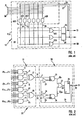
- a conventional PLA cell 10 has input lines 11 through IM which are programmably connectable to the input lines of AND gates AG1 through AGR, which are arranged in a row or first "level” of logic called an AND plane, and which form logical product terms P1 through PR.
- AND plane product term output lines are programmably connectable to OR gates OG1 through OGN, which are arranged in a column or second level called an OR plane, and which provide logical sum-of-product signals on OR plane output lines S1 through SN.
- OR plane output lines S1-SN may be coupled through clocked registers 25, 26 to return signals on feedback lines 27, 28 to AND plane input lines for array cell 10 to execute sequential logic operations.
- the user defines gate input line connections, by way of a pattern for a mask used in a manufacturing step for a mask-programmed PLA, or by way of a "fuse plot" used by a programming machine to blow fuses in a field programmable logic array (FPLA) after manufacture.
- FPLA field programmable logic array
- PLAs are designed with various ratios of quantities of AND gates, OR gates, and programmable connections in input lines to the logic planes.
- One type of PLA a programmable array logic device, for example a "PAL” (registered trademark of Monolithic Memories, Inc.) device, has array input lines programmably connectable to AND plane input lines, and AND plane product output lines fixedly connected to OR plane input lines, with D-type flip-flop output registers.
- PAL registered trademark of Monolithic Memories, Inc.
- D-type flip-flops are powerful, large state machine applications often require the more versatile JK flip-flop function, which starts with a present state value Qo, upon which two input signal values J and K operate to produce a next state value Qo', according to the following table 1:
- the J and/or K signals received by circuit 30 input lines 31 and 32 can in turn be products J1 and K1 of sets of input signals J1a through J1z, and Kla through K1z, respectively, provided by AND gates 11 and 14, Fig. 2. Furthermore, signals J and K can be logical sums of product signals J1 through Jj, and K1 through Kk, which are formed from respective subsets of input signals (a,b,...,z) by AND gates 11 through 16 and OR gates 17 and 18 in a PLA device 10, Fig. 2, without output registers 25 and 26 of Fig. 1.
- an IC 20, Fig. 2, adapted to execute the JK flip-flop function by using a logic array 10 with OR plane output lines connected to a dedicated JK flip-flop circuit 30 cannot provide output signals for functions other than the JK flip-flop function, which conflicts with the IC design goal of making maximum use of minimum circuit elements.
- a PLA device in which a sum-of-products array performs the JK function and stores next state signal Qo' in a D-type flip-flop for output and/or feedback.
- K or its factors Ka...Kz
- Programmable array logic circuits as described in U.S. Patent 4,124,989 are partitioned into cells which include an AND-OR array with a D type flip-flop output register.
- cells include an XOR gate between OR gate output terminals and the D flip-flop input terminal.
- These prior art XOR cells, with multiple AND gates feeding each of two OR gates, are suited to implement bit-carrys for arithmetic operations.
- the third equivalent form of the JK function can be implemented by driving the XOR gate with the previous state output signal Qo applied, without any logical operation, through one of the OR gates-and one associated AND gate, but this use of half the XOR cell is inefficient.
- a programmable array logic cell design optimized for uses such as a flip-flop, a counter, a state machine, or a parity detector.
- the sum signal and the previous state output signal Qo are applied to two input terminals of an XOR gate, which produces present state signal Qo'.
- the cell can be programmed to implement a one bit counter, a Mealy or Moore type state machine, a parity detector, or programmed to implement other functions producing combinatorial or D-type registered output signals.
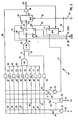
- programmable array logic circuit of this invention is shown in Fig. 3 in a preferred integrated circuit embodiment as cell 60. Details of the fabrication and structure of conventional aspects of programmable array logic circuits are well known in the art.
- cell 60 is mask-programmed during manufacture.
- cell 60 is programmed after manufacture by blowing fuse connections, preferably titanium-tungsten links, although other satisfactory fuses are known.
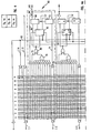
- Cell 60 is preferably embodied in an IC array device 110, Fig. 4, which includes a total of eight identical cells 60.
- Array 110 has 14 array input lines 11 through 114 or -61 which are connected through phase splitters 62 to provide 28 cell input 63 lines to each cell 60.
- each of the eight cells 60 has its output signal coupled through a feedback line and a phase splitter, to provide another 16 cell input lines 63, for a total of 44 cell input lines 63 to each cell.
- Fig. 3 shows only cell feedback input lines 76 and 77 from the feedback line 74 of the illustrated cell 60.
- AND plane input lines 63 are programmably connectable through fuses 64 to the input lines 65 of AND gates 66, 78 and 97.
- the sets of 44 input lines to each AND gate are, for the sake of clarity, shown in Fig. 3 as single lines 65.
- AND gates 66 provide logical product terms P1 through P8 on respective product lines 68 to the input terminals of OR gate 70, from which a sum signal drives one input line 71 to XOR gate 80.
- the second input of XOR gate 80 is connected to output line 79 from AND gate 78, having input lines 65 programmably connectable to receive a signal from any combination of cell input lines 63, including for example the previous state output signal Qo or Qo, as explained below.
- the XOR gate 80 output signal Qo' on line 81 is applied to the data input terminal D of D-type flip-flop 82.
- Cell input line 83 provides a clock signal to the enable terminal of flip-flop 82.
- flip-flop 82 samples the data signal Qo' at its D input terminal, and transfers the data signal value to flip-flop output line 84 as signal Qo.
- Optional multiplexer (MUX) 90 controlled by the voltage on line 92 from programmable fuse 93, either, when fuse 93 is blown, selects line 81 for the Qo' signal presently provided by XOR gate 80 for non- registered output operation of cell 60 (as a Mealy type state machine) or, when fuse 93 is intact, selects flip-flop output line 84 for the Qo signal provided by XOR gate 80 during the previous period of the clock signal (for operation as a Moore type state machine).
- AND gate 97 provides a control signal on line 98 to enable output buffer 99 to transfer the signal from line 91 to cell output line 100.
- output line 100 floats at high impedance, and, if connected to feedback line 74, line 100 can be used as an input line 61 to cell 60.
- AND gate 78 can be used to force line 79 high or low and thereby control line 81 signal polarity.
- a high output signal can be forced from AND gate 78 by blowing all of gate 78 input line 65 fuse connections 64, allowing the disconnected lines 65 to float to the high supply voltage of cell 60, which is equivalent to a logical "true" input signal.
- a low output signal can be forced from AND gate 78 by leaving--intact the fuses 64 between line 78 and both of the pair of complementary lines 63 from any of phase splitters 62.
- a forced zero signal on line 79 disables XOR gate 80 so that, other than a one logic level delay, XOR gate 80 has no effect upon the capability of circuit 60 to perform functions not requiring an XOR gate.
- J and K input signals can be interchanged to control line 81 signal polarity.
- Optional MUX 73 controlled by the voltage on line 92 from programmable fuse 93, either, when fuse 93 is intact, selects the inverting output line 85 from flip-flop 82, which provides the output signal inverse Qo from the preceeding period of the clock or, when fuse 93 is blown, selects cell output line 100. If inverter 99 is supplied by MUX 90 with signal Qo from output line 84 from flip-flop 82, then MUX 73 supplies signal Qo from the preceeding period of the clock. Alternatively, if MUX 90 selects XOR output lead 81, then MUX 73 supplies the present signal Qo'.
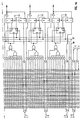
- Any N array input lines 61 can be used for N-bit operation mode signals, to enable appropriate AND gates (66, 78, 97).
- Cell input line 63 connections 64 to AND gate input lines 65 are programmed to decode each combination of mode signals M and their complements to apply all l's to enable appropriate AND gates to form products P of signals on other cell input lines 63. Any cell input lines 63 which are not used in any mode to provide a signal to a given AND gate are disconnected from that AND gate.
- feedback line 76 providing signal Qo is program-connected to an input line 65 of feedback gate 78 and of each AND gate 66 used to form one of products K1 through Kk.
- Feedback line 77 providing signal Qo is program-connected to an input line 65 of each of the AND gates 66 used to find one of products J1 through Jj.
- JK operations are executed by cell 60 using other mode signals M and data signals D as listed in Table 3.
- logical 1 signals applied to optional control lines 86 or 87 set or reset flip-flop 82, respectively.
- a logical 1 product term applied to input line 71 of XOR gate 80 toggles output line 81 signal Qo'.
- a logical 1 product on line 71 can be assured by applying logical l's to all the input lines of at least one J product gate 66 and of at least one K product gate 66, or to a dedicated AND gate 67 selected by a toggle-mode signal.
- cell 60 can be programmed for use as a counter in a bank of similar counter cells 60 (not shown) linked to carry each less significant cell 60 output signal Qo' to an input line 61 of the next higher significance bit-counting cell 60.
- Input signals M1, M2, and M3 are used as three bit mode signals arbitrarily assigned to designate eight operations to be performed upon other input signals Q, D, and their inverses, as shown in Table 2.
- Mode signals M1, M2, M3 are decoded by the three cells 60 as listed in the following Table 3.
- Such a multi-cell counter can, for example, load, increment, decrement, clear, set, hold, or jump to, a value of Q.
- the least significant bit counter 60 jumps to 1, the middle significance bit counter 60 to 0, and the most significant bit counter 60 to 1.
- Two product terms are used for the load mode code 000.
- the eighth code 111 for "hold" cannot be decoded. But if a mode signal equal to 111 is applied to mode input lines 61 to each cell 60, no other operation is decoded and the value of signal Qo from each cell is held.
Landscapes
- Logic Circuits (AREA)
- Design And Manufacture Of Integrated Circuits (AREA)
Applications Claiming Priority (2)
| Application Number | Priority Date | Filing Date | Title |
|---|---|---|---|
| US06/864,185 US4789951A (en) | 1986-05-16 | 1986-05-16 | Programmable array logic cell |
| US864185 | 1986-05-16 |
Publications (3)
| Publication Number | Publication Date |
|---|---|
| EP0245884A2 true EP0245884A2 (de) | 1987-11-19 |
| EP0245884A3 EP0245884A3 (en) | 1987-12-23 |
| EP0245884B1 EP0245884B1 (de) | 1994-02-02 |
Family
ID=25342707
Family Applications (1)
| Application Number | Title | Priority Date | Filing Date |
|---|---|---|---|
| EP87200415A Expired - Lifetime EP0245884B1 (de) | 1986-05-16 | 1987-03-06 | Programmierbare Array-Logik-Zelle |
Country Status (4)
| Country | Link |
|---|---|
| US (1) | US4789951A (de) |
| EP (1) | EP0245884B1 (de) |
| JP (1) | JP2628996B2 (de) |
| DE (1) | DE3788974T2 (de) |
Cited By (3)
| Publication number | Priority date | Publication date | Assignee | Title |
|---|---|---|---|---|
| EP0385482A3 (de) * | 1989-03-03 | 1992-03-04 | Kabushiki Kaisha Toshiba | In einer integrierten MOS-Logikschaltung verwendete Eingangsschalteinrichtung |
| US5168177A (en) * | 1985-12-06 | 1992-12-01 | Advanced Micro Devices, Inc. | Programmable logic device with observability and preloadability for buried state registers |
| EP1547248A4 (de) * | 2002-09-20 | 2006-08-23 | Atmel Corp | Architektur für einen programmierbaren logikbaustein (pld) für hohe geschwindigkeiten und null gleichstromleistung |
Families Citing this family (57)
| Publication number | Priority date | Publication date | Assignee | Title |
|---|---|---|---|---|
| US4896296A (en) * | 1985-03-04 | 1990-01-23 | Lattice Semiconductor Corporation | Programmable logic device configurable input/output cell |
| US5225719A (en) * | 1985-03-29 | 1993-07-06 | Advanced Micro Devices, Inc. | Family of multiple segmented programmable logic blocks interconnected by a high speed centralized switch matrix |
| US4963768A (en) * | 1985-03-29 | 1990-10-16 | Advanced Micro Devices, Inc. | Flexible, programmable cell array interconnected by a programmable switch matrix |
| US5451887A (en) * | 1986-09-19 | 1995-09-19 | Actel Corporation | Programmable logic module and architecture for field programmable gate array device |
| US5367208A (en) | 1986-09-19 | 1994-11-22 | Actel Corporation | Reconfigurable programmable interconnect architecture |
| US5477165A (en) * | 1986-09-19 | 1995-12-19 | Actel Corporation | Programmable logic module and architecture for field programmable gate array device |
| JPH01259274A (ja) * | 1988-04-08 | 1989-10-16 | Fujitsu Ltd | 集積回路の試験方式 |
| US4903223A (en) * | 1988-05-05 | 1990-02-20 | Altera Corporation | Programmable logic device with programmable word line connections |
| US5023484A (en) * | 1988-09-02 | 1991-06-11 | Cypress Semiconductor Corporation | Architecture of high speed synchronous state machine |
| US4879481A (en) * | 1988-09-02 | 1989-11-07 | Cypress Semiconductor Corporation | Dual I/O macrocell for high speed synchronous state machine |
| US4987319A (en) * | 1988-09-08 | 1991-01-22 | Kawasaki Steel Corporation | Programmable input/output circuit and programmable logic device |
| US4914322A (en) * | 1988-12-16 | 1990-04-03 | Advanced Micro Devices, Inc. | Polarity option control logic for use with a register of a programmable logic array macrocell |
| US5457409A (en) * | 1992-08-03 | 1995-10-10 | Advanced Micro Devices, Inc. | Architecture of a multiple array high density programmable logic device with a plurality of programmable switch matrices |
| US5489857A (en) * | 1992-08-03 | 1996-02-06 | Advanced Micro Devices, Inc. | Flexible synchronous/asynchronous cell structure for a high density programmable logic device |
| US5027011A (en) * | 1989-10-31 | 1991-06-25 | Sgs-Thomson Microelectronics, Inc. | Input row drivers for programmable logic devices |
| US5144582A (en) * | 1990-03-30 | 1992-09-01 | Sgs-Thomson Microelectronics, Inc. | Sram based cell for programmable logic devices |
| US5198705A (en) * | 1990-05-11 | 1993-03-30 | Actel Corporation | Logic module with configurable combinational and sequential blocks |
| US5055718A (en) * | 1990-05-11 | 1991-10-08 | Actel Corporation | Logic module with configurable combinational and sequential blocks |
| WO1994029784A1 (en) * | 1990-11-15 | 1994-12-22 | Edward Hyman | Method and apparatus for compiling and implementing state-machine states and outputs for a cellular array |
| JP2563679B2 (ja) * | 1991-01-24 | 1996-12-11 | シャープ株式会社 | 双方向入出力信号分離回路 |
| US5117132A (en) * | 1991-02-08 | 1992-05-26 | Unisys Corporation | Flexible utilization of general flip-flops in programmable array logic |
| US5122685A (en) * | 1991-03-06 | 1992-06-16 | Quicklogic Corporation | Programmable application specific integrated circuit and logic cell therefor |
| US5416367A (en) * | 1991-03-06 | 1995-05-16 | Quicklogic Corporation | Programmable application specific integrated circuit and logic cell therefor |
| US5861760A (en) * | 1991-04-25 | 1999-01-19 | Altera Corporation | Programmable logic device macrocell with improved capability |
| US5191243A (en) * | 1991-05-06 | 1993-03-02 | Lattice Semiconductor Corporation | Output logic macrocell with enhanced functional capabilities |
| DE69227144T2 (de) * | 1991-05-10 | 1999-03-18 | Kabushiki Kaisha Toshiba, Kawasaki, Kanagawa | Programmierbare logische Einheit |
| US5231312A (en) * | 1992-03-12 | 1993-07-27 | Atmel Corporation | Integrated logic circuit with functionally flexible input/output macrocells |
| US5300830A (en) * | 1992-05-15 | 1994-04-05 | Micron Semiconductor, Inc. | Programmable logic device macrocell with an exclusive feedback and exclusive external input lines for registered and combinatorial modes using a dedicated product term for control |
| US5384500A (en) * | 1992-05-15 | 1995-01-24 | Micron Semiconductor, Inc. | Programmable logic device macrocell with an exclusive feedback and an exclusive external input line for a combinatorial mode and accommodating two separate programmable or planes |
| US5331227A (en) * | 1992-05-15 | 1994-07-19 | Micron Semiconductor, Inc. | Programmable logic device macrocell with an exclusive feedback line and an exclusive external input line |
| US5287017A (en) * | 1992-05-15 | 1994-02-15 | Micron Technology, Inc. | Programmable logic device macrocell with two OR array inputs |
| US5298803A (en) * | 1992-07-15 | 1994-03-29 | Micron Semiconductor, Inc. | Programmable logic device having low power microcells with selectable registered and combinatorial output signals |
| EP0584910B1 (de) * | 1992-08-03 | 1996-09-04 | Advanced Micro Devices, Inc. | Programmierbare logische Vorrichtung |
| US5386155A (en) * | 1993-03-30 | 1995-01-31 | Intel Corporation | Apparatus and method for selecting polarity and output type in a programmable logic device |
| US5440247A (en) * | 1993-05-26 | 1995-08-08 | Kaplinsky; Cecil H. | Fast CMOS logic with programmable logic control |
| US5742179A (en) * | 1994-01-27 | 1998-04-21 | Dyna Logic Corporation | High speed programmable logic architecture |
| US5646546A (en) * | 1995-06-02 | 1997-07-08 | International Business Machines Corporation | Programmable logic cell having configurable gates and multiplexers |
| US5617041A (en) * | 1995-06-02 | 1997-04-01 | Xilinx, Inc. | Method and apparatus for reducing coupling switching noise in interconnect array matrix |
| US5818254A (en) * | 1995-06-02 | 1998-10-06 | Advanced Micro Devices, Inc. | Multi-tiered hierarchical high speed switch matrix structure for very high-density complex programmable logic devices |
| US5521529A (en) * | 1995-06-02 | 1996-05-28 | Advanced Micro Devices, Inc. | Very high-density complex programmable logic devices with a multi-tiered hierarchical switch matrix and optimized flexible logic allocation |
| US6028446A (en) * | 1995-06-06 | 2000-02-22 | Advanced Micro Devices, Inc. | Flexible synchronous and asynchronous circuits for a very high density programmable logic device |
| US5773994A (en) * | 1995-12-15 | 1998-06-30 | Cypress Semiconductor Corp. | Method and apparatus for implementing an internal tri-state bus within a programmable logic circuit |
| US5744980A (en) * | 1996-02-16 | 1998-04-28 | Actel Corporation | Flexible, high-performance static RAM architecture for field-programmable gate arrays |
| JPH09232946A (ja) * | 1996-02-26 | 1997-09-05 | Mitsubishi Electric Corp | カウンタ |
| US5986465A (en) * | 1996-04-09 | 1999-11-16 | Altera Corporation | Programmable logic integrated circuit architecture incorporating a global shareable expander |
| US5781032A (en) * | 1996-09-09 | 1998-07-14 | International Business Machines Corporation | Programmable inverter circuit used in a programmable logic cell |
| US5936426A (en) * | 1997-02-03 | 1999-08-10 | Actel Corporation | Logic function module for field programmable array |
| US6467009B1 (en) | 1998-10-14 | 2002-10-15 | Triscend Corporation | Configurable processor system unit |
| US6259273B1 (en) | 1999-06-15 | 2001-07-10 | Ict Acquisition Corp. | Programmable logic device with mixed mode programmable logic array |
| US6721840B1 (en) | 2000-08-18 | 2004-04-13 | Triscend Corporation | Method and system for interfacing an integrated circuit to synchronous dynamic memory and static memory |
| US6725364B1 (en) | 2001-03-08 | 2004-04-20 | Xilinx, Inc. | Configurable processor system |
| AU2003244975A1 (en) * | 2002-07-08 | 2004-01-23 | Koninklijke Philips Electronics N.V. | Electronic circuit with test unit for testing interconnects |
| US6747480B1 (en) | 2002-07-12 | 2004-06-08 | Altera Corporation | Programmable logic devices with bidirect ional cascades |
| US20100106959A1 (en) * | 2005-12-16 | 2010-04-29 | Pmc Sierra Ltd. | Triple and quadruple churning security for 1G and 10G PON |
| US7893772B1 (en) | 2007-12-03 | 2011-02-22 | Cypress Semiconductor Corporation | System and method of loading a programmable counter |
| US9231594B2 (en) | 2011-12-21 | 2016-01-05 | Ecole Polytechnique Federale De Lausanne (Epfl) | Non-LUT field-programmable gate arrays |
| FR3022410B1 (fr) * | 2014-06-12 | 2016-05-27 | Delphi Int Operations Luxembourg Sarl | Connecteur electrique blinde et son procede de fabrication |
Citations (1)
| Publication number | Priority date | Publication date | Assignee | Title |
|---|---|---|---|---|
| US4124989A (en) | 1975-06-04 | 1978-11-14 | Redpath Dorman Long (North Sea) Limited | Supports for maritime structures |
Family Cites Families (6)
| Publication number | Priority date | Publication date | Assignee | Title |
|---|---|---|---|---|
| US4124489A (en) * | 1977-02-16 | 1978-11-07 | Exxon Research & Engineering Co. | Production of transformer oil feed stocks from waxy crudes |
| US4124899A (en) * | 1977-05-23 | 1978-11-07 | Monolithic Memories, Inc. | Programmable array logic circuit |
| DE3582990D1 (de) * | 1984-09-28 | 1991-07-04 | Advanced Micro Devices Inc | Logikschaltung mit dynamisch steuerbarem ausgang. |
| US4684830A (en) * | 1985-03-22 | 1987-08-04 | Monolithic Memories, Inc. | Output circuit for a programmable logic array |
| US4677318A (en) * | 1985-04-12 | 1987-06-30 | Altera Corporation | Programmable logic storage element for programmable logic devices |
| US4644192A (en) * | 1985-09-19 | 1987-02-17 | Harris Corporation | Programmable array logic with shared product terms and J-K registered outputs |
-
1986
- 1986-05-16 US US06/864,185 patent/US4789951A/en not_active Expired - Lifetime
-
1987
- 1987-03-06 EP EP87200415A patent/EP0245884B1/de not_active Expired - Lifetime
- 1987-03-06 DE DE3788974T patent/DE3788974T2/de not_active Expired - Fee Related
- 1987-05-15 JP JP62117193A patent/JP2628996B2/ja not_active Expired - Lifetime
Patent Citations (1)
| Publication number | Priority date | Publication date | Assignee | Title |
|---|---|---|---|---|
| US4124989A (en) | 1975-06-04 | 1978-11-14 | Redpath Dorman Long (North Sea) Limited | Supports for maritime structures |
Cited By (3)
| Publication number | Priority date | Publication date | Assignee | Title |
|---|---|---|---|---|
| US5168177A (en) * | 1985-12-06 | 1992-12-01 | Advanced Micro Devices, Inc. | Programmable logic device with observability and preloadability for buried state registers |
| EP0385482A3 (de) * | 1989-03-03 | 1992-03-04 | Kabushiki Kaisha Toshiba | In einer integrierten MOS-Logikschaltung verwendete Eingangsschalteinrichtung |
| EP1547248A4 (de) * | 2002-09-20 | 2006-08-23 | Atmel Corp | Architektur für einen programmierbaren logikbaustein (pld) für hohe geschwindigkeiten und null gleichstromleistung |
Also Published As
| Publication number | Publication date |
|---|---|
| JP2628996B2 (ja) | 1997-07-09 |
| DE3788974T2 (de) | 1994-05-19 |
| EP0245884A3 (en) | 1987-12-23 |
| EP0245884B1 (de) | 1994-02-02 |
| US4789951A (en) | 1988-12-06 |
| JPS62281517A (ja) | 1987-12-07 |
| DE3788974D1 (de) | 1994-03-17 |
Similar Documents
| Publication | Publication Date | Title |
|---|---|---|
| EP0245884B1 (de) | Programmierbare Array-Logik-Zelle | |
| US5523706A (en) | High speed, low power macrocell | |
| KR940010679B1 (ko) | 프로그램식 논리 회로를 포함한 집적회로 | |
| EP0340891B1 (de) | Programmierbare logische Vorrichtung mit programmierbaren Wortlinien-Verbindungen | |
| US4963768A (en) | Flexible, programmable cell array interconnected by a programmable switch matrix | |
| US5302866A (en) | Input circuit block and method for PLDs with register clock enable selection | |
| US6028808A (en) | Programmable logic array integrated circuits | |
| EP0198677B1 (de) | Programmierbares logisches Speicherelement für programmierbare logische Einrichtungen | |
| US6353331B1 (en) | Complex programmable logic device with lookup table | |
| EP0225715B1 (de) | Programmierbare Eingangs/Ausgangszelle | |
| EP0472650B1 (de) | Logisch programmierbare ausdehnungsvorrichtung | |
| JPH07504797A (ja) | 論理積項の縦続接続および改良したフリップフロップ利用を伴うマクロセル | |
| US4675556A (en) | Binomially-encoded finite state machine | |
| JPH08330943A (ja) | 組合せ回路または順序回路として構成されうるフィールドプログラマブル・ゲートアレイ論理モジュール | |
| EP0472594B1 (de) | Programmierbare logische gatter | |
| US5153462A (en) | Programmable logic device incorporating voltage comparator | |
| US6714057B2 (en) | Multi-purpose digital frequency synthesizer circuit for a programmable logic device | |
| US5497107A (en) | Multiple, selectable PLAS having shared inputs and outputs | |
| US5027012A (en) | Programmable logic circuit using wired-or tristate gates | |
| US4516251A (en) | Programmable prescaler | |
| US5298803A (en) | Programmable logic device having low power microcells with selectable registered and combinatorial output signals | |
| US4644192A (en) | Programmable array logic with shared product terms and J-K registered outputs | |
| EP0733285B1 (de) | Kombinierte pla- und pal-schaltung | |
| EP0085489B1 (de) | Schaltung einer Speicher enthaltende Logikanordnung | |
| US5523705A (en) | Apparatus and method for selecting and buffering inputs of programmable logic devices |
Legal Events
| Date | Code | Title | Description |
|---|---|---|---|
| PUAI | Public reference made under article 153(3) epc to a published international application that has entered the european phase |
Free format text: ORIGINAL CODE: 0009012 |
|
| PUAL | Search report despatched |
Free format text: ORIGINAL CODE: 0009013 |
|
| AK | Designated contracting states |
Kind code of ref document: A2 Designated state(s): DE FR GB NL |
|
| AK | Designated contracting states |
Kind code of ref document: A3 Designated state(s): DE FR GB NL |
|
| 17P | Request for examination filed |
Effective date: 19880603 |
|
| RAP1 | Party data changed (applicant data changed or rights of an application transferred) |
Owner name: ADVANCED MICRO DEVICES, INC. |
|
| 17Q | First examination report despatched |
Effective date: 19900319 |
|
| GRAA | (expected) grant |
Free format text: ORIGINAL CODE: 0009210 |
|
| AK | Designated contracting states |
Kind code of ref document: B1 Designated state(s): DE FR GB NL |
|
| REF | Corresponds to: |
Ref document number: 3788974 Country of ref document: DE Date of ref document: 19940317 |
|
| ET | Fr: translation filed | ||
| PLBE | No opposition filed within time limit |
Free format text: ORIGINAL CODE: 0009261 |
|
| STAA | Information on the status of an ep patent application or granted ep patent |
Free format text: STATUS: NO OPPOSITION FILED WITHIN TIME LIMIT |
|
| 26N | No opposition filed | ||
| PGFP | Annual fee paid to national office [announced via postgrant information from national office to epo] |
Ref country code: NL Payment date: 20011214 Year of fee payment: 16 |
|
| REG | Reference to a national code |
Ref country code: GB Ref legal event code: IF02 |
|
| PGFP | Annual fee paid to national office [announced via postgrant information from national office to epo] |
Ref country code: GB Payment date: 20020205 Year of fee payment: 16 |
|
| PGFP | Annual fee paid to national office [announced via postgrant information from national office to epo] |
Ref country code: FR Payment date: 20020228 Year of fee payment: 16 |
|
| PGFP | Annual fee paid to national office [announced via postgrant information from national office to epo] |
Ref country code: DE Payment date: 20020327 Year of fee payment: 16 |
|
| PG25 | Lapsed in a contracting state [announced via postgrant information from national office to epo] |
Ref country code: GB Free format text: LAPSE BECAUSE OF NON-PAYMENT OF DUE FEES Effective date: 20030306 |
|
| PG25 | Lapsed in a contracting state [announced via postgrant information from national office to epo] |
Ref country code: NL Free format text: LAPSE BECAUSE OF NON-PAYMENT OF DUE FEES Effective date: 20031001 Ref country code: DE Free format text: LAPSE BECAUSE OF NON-PAYMENT OF DUE FEES Effective date: 20031001 |
|
| GBPC | Gb: european patent ceased through non-payment of renewal fee |
Effective date: 20030306 |
|
| PG25 | Lapsed in a contracting state [announced via postgrant information from national office to epo] |
Ref country code: FR Free format text: LAPSE BECAUSE OF NON-PAYMENT OF DUE FEES Effective date: 20031127 |
|
| NLV4 | Nl: lapsed or anulled due to non-payment of the annual fee |
Effective date: 20031001 |
|
| REG | Reference to a national code |
Ref country code: FR Ref legal event code: ST |
|
| APAH | Appeal reference modified |
Free format text: ORIGINAL CODE: EPIDOSCREFNO |