EP0245591A2 - Verfahren und Gerät zur Nachrichtenübertragung zu elektronischen Systemen - Google Patents
Verfahren und Gerät zur Nachrichtenübertragung zu elektronischen Systemen Download PDFInfo
- Publication number
- EP0245591A2 EP0245591A2 EP87102427A EP87102427A EP0245591A2 EP 0245591 A2 EP0245591 A2 EP 0245591A2 EP 87102427 A EP87102427 A EP 87102427A EP 87102427 A EP87102427 A EP 87102427A EP 0245591 A2 EP0245591 A2 EP 0245591A2
- Authority
- EP
- European Patent Office
- Prior art keywords
- power supply
- voltage
- information
- variations
- bit stream
- Prior art date
- Legal status (The legal status is an assumption and is not a legal conclusion. Google has not performed a legal analysis and makes no representation as to the accuracy of the status listed.)
- Withdrawn
Links
Images
Classifications
-
- G—PHYSICS
- G06—COMPUTING OR CALCULATING; COUNTING
- G06F—ELECTRIC DIGITAL DATA PROCESSING
- G06F15/00—Digital computers in general; Data processing equipment in general
-
- G—PHYSICS
- G11—INFORMATION STORAGE
- G11C—STATIC STORES
- G11C29/00—Checking stores for correct operation ; Subsequent repair; Testing stores during standby or offline operation
- G11C29/04—Detection or location of defective memory elements, e.g. cell constructio details, timing of test signals
- G11C29/08—Functional testing, e.g. testing during refresh, power-on self testing [POST] or distributed testing
- G11C29/48—Arrangements in static stores specially adapted for testing by means external to the store, e.g. using direct memory access [DMA] or using auxiliary access paths
-
- G—PHYSICS
- G06—COMPUTING OR CALCULATING; COUNTING
- G06F—ELECTRIC DIGITAL DATA PROCESSING
- G06F11/00—Error detection; Error correction; Monitoring
- G06F11/22—Detection or location of defective computer hardware by testing during standby operation or during idle time, e.g. start-up testing
- G06F11/26—Functional testing
- G06F11/273—Tester hardware, i.e. output processing circuits
- G06F11/2733—Test interface between tester and unit under test
-
- G—PHYSICS
- G06—COMPUTING OR CALCULATING; COUNTING
- G06F—ELECTRIC DIGITAL DATA PROCESSING
- G06F13/00—Interconnection of, or transfer of information or other signals between, memories, input/output devices or central processing units
- G06F13/38—Information transfer, e.g. on bus
Definitions
- This invention relates to the field of data processing, and more particularly to a method for transferring data between electronic devices.
- the invention is especially adapted to testing systems comprising electronic devices, however, the invention is equally useful for transferring data into electronic devices under any condition.
- Data processing systems typically consist of a central processing unit (CPU), RAM, ROM, and one or more input and output devices such as a keyboard and display.
- CPU central processing unit
- RAM random access memory
- ROM read-only memory
- input and output devices such as a keyboard and display.
- Testing a device during its manufacture is necessary in order to provide reliable high quality products.
- testing the product does not necessarily enhance the marketability of a product, so it is not always desirable to dedicate a pin of an integrated circuit or program space in a ROM in order to test a product for manufacturing defects.
- Prior art solutions include mounting a test ROM in the test system fixture or programming the test system to intercept signals from the CPU for a particular address and then substitute the appropriate instructions from the test program. These test approaches require access to system status information or a very sophisticated expensive test system or both.
- an apparatus and method for transferring data into an integrated circuit.
- the apparatus comprises a low power supply detection unit, a serial-to-parallel converter unit and a control unit.
- the low power supply detection unit is used to demodulate the power supply line to generate a serial bit stream.
- the bit stream is then converted to parallel data using any of several well known techniques including FM, MFM, and NRZ.
- the logic control unit disposes of the data as desired by the designer.
- Such an apparatus and method may be used, among other things, to transfer a program into RAM which may be used to test a product.
- the apparatus is included along with the typical storage array and decode circuitry to form a RAM.
- a test system may then modulate the power supply voltage of the system under test to load the program.
- the program then performs the manufacturing test on the system.
- the primary object of the present invention is to provide a means for transferring data into a device without dedicating a pin of the integrated circuit or other separate input line in the device for the purpose.
- Another object of the present invention is to add the least amount of circuitry to the system device employing the method and apparatus.
- a further object of the present invention is to permit economical testing of a system.
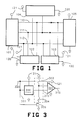
- FIG. 1 is a functional block diagram of a computer system employing the method and apparatus of present invention.
- the system comprises a central processing unit (CPU) 101, RAM 102, ROM 103, display 104 and keyboard 105, collectively known as system devices. Communication between the system devices is provided on data bus 110, address bus 111 and control bus 112.
- the CPU is capable of executing code located in either ROM 103 or RAM 102. Power is supplied to each of the system devices by voltage supply line 121 and ground line 120. All the system devices are located on a single system card.
- the system card In order to test the computer system, the system card is placed on a test fixture and the test program is loaded into the RAM and executed. As the program is executed by the CPU 101, the results are displayed on the display 104.
- FIG. 2 is a functional block diagram of a RAM device in accordance with the preferred embodiment of the present invention.
- the RAM 102 has two power supply lines, voltage supply line 121 and ground line 120. These supply lines supply the power to each of the functional units located in the RAM.
- the RAM 102 comprises a low power supply detection unit 201, serial-to-parallel converter unit 202, control unit 205, address decode unit 203 and storage array 204.
- the low power supply detection unit 201 is connected between the power supply lines 120 and 121.
- the unit 201 generates a stream of logic bits from variations in the voltage across the power supply lines.
- the bit stream is then supplied to the serial-to-parallel converter unit 202.
- the serial-to-parallel converter unit 202 can use any of the available serial-to-parallel encoding techniques including biphase, FM, MFM, NRZ.
- the encoding technique may or may not be self clocking.
- control logic 105 transfers the data to the storage array 204 over data bus 110.
- Normal operation of the RAM is performed by supplying an address to be read or written on the address bus 111.
- control signals provided on control bus 112 data is then either read from the data bus 110 or supplied to the data bus 110 by the storage array 204.
- the address bus 111, data bus 110 and control bus 112 may be implemented as serial or parallel busses and may by multiplexed according to the wishes of the designer.
- the CPU 101 performs the serial-to-parallel conversion under control of software.
- the CPU 101 executes a program contained in ROM 103 which repeatedly scans the output from the low power supply detection unit 201 to receive each bit of information, assembles the bits into the data, and stores the information in RAM 102.
- asynchronous NRZ technique is employed which is similar to RS-232.
- FIG. 3 is a low power supply detection unit in accordance with the preferred embodiment of the present invention.
- the circuit comprises voltage reference 300, a voltage divider 312, switch 305 and comparator 301.
- the voltage divider 312 comprises resistors 303 and 304.
- a power control signal 302 disables the voltage reference 300 and comparator 301 in order to save power when they are not in use. This function is optional.
- the voltage reference 300 generates a reference voltage independent of the voltage on supply line 121. This reference voltage serves as the low voltage threshold for determining when, for example, the batteries in the system need to be replaced.
- a voltage divider comprising resistors 302 and 303 also generates a reference voltage, however this voltage is related to the voltage across the power supply lines 121 and 120.
- the voltage divider may be disabled by switch 305 under control of power control signal 302 in order to conserve power.
- the reference voltages from the voltage divider 312 and from the voltage reference 300 are compared by comparator 301 which generates an output signal 315.
- the output signal 315 is logic false when the voltage supply line 121 is above the low voltage threshold and logic true when the voltage supply line 121 is below the low voltage threshold.
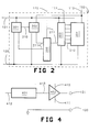
- FIG. 4 is a functional block diagram of a test system compatible with the preferred embodiment of the present invention.
- the circuit comprises a parallel-to- serial converter 401 and a driver 402.
- the parallel-to-serial converter 401 generates a bit stream from data supplied to it over bus 412 using an encoding technique which is compatible with the techniques employed in the system under test.
- the driver 402 modulates the power supply voltage with the bit stream generated by the parallel-to-serial converter 401.
- the driver 402 acts as the power supply for the system under test and modulates the power supply voltage by switching between two voltage levels 410 and 411, both of which are within the range of acceptable power supply voltages, in response to the true and false logic levels of the bit stream.
- Voltage level 410 is greater than the low voltage threshold determined by the voltage reference 300 of the low power detection unit 201 and the voltage level 411 is less than the low voltage threshold.
- the output of the driver is fed to the voltage supply line of the system under test.
- the operation of the preferred embodiment when employed in a test system is as follows.
- the test program located in the memory of the test system is fed down the parallel bus 412 to the parallel-to-serial converter 401.
- the parallel-to-serial converter encodes the program to generate a bit stream which is send to the driver 402.
- the driver 402 modulates the voltage supply line 121 based on the bit stream.
- the modulated power supply lines are fed to the system under test. Since each system device in the system is designed to operate with a varying voltage supply, the operation of the system is unaffected by the fluctuations in voltage of the power supply lines.
- the CPU 101 periodically activates the low power supply detection unit 201 until the CPU recognizes that data is ready to be loaded.
- the low power supply detection unit 201 translates the modulated voltage on the power supply lines 121 and 120 into a bit stream which is converted into a series of parallel bytes by the serial-to-parallel converter 202. This data is stored in the storage array 204 under the control of control unit 105.
- the CPU 101 waits for the loading process to be completed and then executes the test code just loaded thereby performing the manufacturing test. The results of the test are displayed on the display 104.
- a low power supply condition may be discovered using the low power supply detection unit 201 when the voltage of the power supply line is below the low voltage threshold for a period of time longer than permitted by the encoding technique.
- the method and apparatus disclosed herein is equally applicable to testing any of the system devices, for example, the CPU 101 and ROM 103 or any other electronic device with a power supply input.
- the method and apparatus of the present invention are not limited to use in device testing.
- the method and apparatus may generally be used to transfer information, including programs, data and control into electronic systems.
- the method and apparatus could be used to program an EPROM in a system by transferring data into the EPROM on the power supply and then raising the supply voltage to program the EPROM.
- the method and apparatus may also be used to transfer information including programs, data and control into a device during normal operation.
- the method and apparatus are compatible with battery operation and AC line operation. Additional applications of the present invention are readily apparent to those skilled in the art.
Landscapes
- Engineering & Computer Science (AREA)
- Theoretical Computer Science (AREA)
- General Engineering & Computer Science (AREA)
- Physics & Mathematics (AREA)
- General Physics & Mathematics (AREA)
- Computer Hardware Design (AREA)
- Quality & Reliability (AREA)
- Tests Of Electronic Circuits (AREA)
- Power Sources (AREA)
- Test And Diagnosis Of Digital Computers (AREA)
- Techniques For Improving Reliability Of Storages (AREA)
Applications Claiming Priority (2)
| Application Number | Priority Date | Filing Date | Title |
|---|---|---|---|
| US06/863,673 US4774493A (en) | 1986-05-15 | 1986-05-15 | Method and apparatus for transferring information into electronic systems |
| US863673 | 1986-05-15 |
Publications (2)
| Publication Number | Publication Date |
|---|---|
| EP0245591A2 true EP0245591A2 (de) | 1987-11-19 |
| EP0245591A3 EP0245591A3 (de) | 1989-11-02 |
Family
ID=25341556
Family Applications (1)
| Application Number | Title | Priority Date | Filing Date |
|---|---|---|---|
| EP87102427A Withdrawn EP0245591A3 (de) | 1986-05-15 | 1987-02-20 | Verfahren und Gerät zur Nachrichtenübertragung zu elektronischen Systemen |
Country Status (4)
| Country | Link |
|---|---|
| US (1) | US4774493A (de) |
| EP (1) | EP0245591A3 (de) |
| JP (1) | JPS62267839A (de) |
| KR (1) | KR870011545A (de) |
Cited By (1)
| Publication number | Priority date | Publication date | Assignee | Title |
|---|---|---|---|---|
| DE102006022985A1 (de) * | 2006-05-15 | 2007-11-22 | Micronas Gmbh | Schaltungsanordnung mit einer seriellen Testschnittstelle bzw. serielles Testbetriebsverfahren |
Families Citing this family (16)
| Publication number | Priority date | Publication date | Assignee | Title |
|---|---|---|---|---|
| DE68925271T2 (de) * | 1988-10-27 | 1996-08-14 | Texas Instruments Inc | Kommunikations-, Informations-, Wartungsdiagnostik und Ausbildungssystem |
| US5432429A (en) * | 1990-10-23 | 1995-07-11 | Benchmarq Microelectronics, Inc. | System for charging/monitoring batteries for a microprocessor based system |
| US6377028B1 (en) | 1990-10-23 | 2002-04-23 | Texas Instruments Incorporated | System for charging monitoring batteries for a microprocessor based method |
| US5357203A (en) * | 1992-07-08 | 1994-10-18 | Benchmarq Microelectronics, Inc. | Battery monitoring circuit for operating with high battery discharge rates |
| US5284719A (en) * | 1992-07-08 | 1994-02-08 | Benchmarq Microelectronics, Inc. | Method and apparatus for monitoring battery capacity |
| US5440221A (en) * | 1992-07-08 | 1995-08-08 | Benchmarg Microelectronics, Inc. | Method and apparatus for monitoring batttery capacity with charge control |
| US5553070A (en) * | 1994-09-13 | 1996-09-03 | Riley; Robert E. | Data link module for time division multiplexing control systems |
| US5818821A (en) | 1994-12-30 | 1998-10-06 | Intelogis, Inc. | Universal lan power line carrier repeater system and method |
| US5970127A (en) * | 1997-10-16 | 1999-10-19 | Phonex Corporation | Caller identification system for wireless phone jacks and wireless modem jacks |
| US6055435A (en) | 1997-10-16 | 2000-04-25 | Phonex Corporation | Wireless telephone connection surge suppressor |
| US6107912A (en) * | 1997-12-08 | 2000-08-22 | Phonex Corporation | Wireless modem jack |
| US6246868B1 (en) | 1998-08-14 | 2001-06-12 | Phonex Corporation | Conversion and distribution of incoming wireless telephone signals using the power line |
| US6243571B1 (en) | 1998-09-21 | 2001-06-05 | Phonex Corporation | Method and system for distribution of wireless signals for increased wireless coverage using power lines |
| US20030018892A1 (en) * | 2001-07-19 | 2003-01-23 | Jose Tello | Computer with a modified north bridge, security engine and smart card having a secure boot capability and method for secure booting a computer |
| US7614737B2 (en) * | 2005-12-16 | 2009-11-10 | Lexmark International Inc. | Method for identifying an installed cartridge |
| US8418012B2 (en) | 2010-09-21 | 2013-04-09 | Ansaldo Sts Usa, Inc. | Method of analyzing the safety of a device employing on target hardware description language based fault injection |
Family Cites Families (6)
| Publication number | Priority date | Publication date | Assignee | Title |
|---|---|---|---|---|
| US4171539A (en) * | 1977-12-19 | 1979-10-16 | The Bendix Corporation | Power strobed digital computer system |
| JPS54134341A (en) * | 1978-04-10 | 1979-10-18 | Nippon Denso Co | Power supply system monitoring method and apparatus for vehicles |
| JPS56162122A (en) * | 1980-05-16 | 1981-12-12 | Canon Inc | Electronic apparatus equipped with printing device |
| FR2509889A1 (fr) * | 1981-07-17 | 1983-01-21 | Asulab Sa | Installation de collecte de donnees |
| US4466074A (en) * | 1981-09-18 | 1984-08-14 | Mcgraw-Edison Company | Power outage timer |
| US4553081A (en) * | 1982-06-07 | 1985-11-12 | Norand Corporation | Portable battery powered system |
-
1986
- 1986-05-15 US US06/863,673 patent/US4774493A/en not_active Expired - Fee Related
-
1987
- 1987-02-20 EP EP87102427A patent/EP0245591A3/de not_active Withdrawn
- 1987-04-28 JP JP62107853A patent/JPS62267839A/ja active Pending
- 1987-05-14 KR KR870004718A patent/KR870011545A/ko not_active Withdrawn
Cited By (2)
| Publication number | Priority date | Publication date | Assignee | Title |
|---|---|---|---|---|
| DE102006022985A1 (de) * | 2006-05-15 | 2007-11-22 | Micronas Gmbh | Schaltungsanordnung mit einer seriellen Testschnittstelle bzw. serielles Testbetriebsverfahren |
| US7761756B2 (en) | 2006-05-15 | 2010-07-20 | Micronas Gmbh | Circuit configuration with serial test interface or serial test operating-mode procedure |
Also Published As
| Publication number | Publication date |
|---|---|
| EP0245591A3 (de) | 1989-11-02 |
| KR870011545A (ko) | 1987-12-24 |
| JPS62267839A (ja) | 1987-11-20 |
| US4774493A (en) | 1988-09-27 |
Similar Documents
| Publication | Publication Date | Title |
|---|---|---|
| US4774493A (en) | Method and apparatus for transferring information into electronic systems | |
| EP1087404B1 (de) | Verfahren, System und Vorrichtung zum Bestimmen dass ein Programmierspannungspegel ausreichend zur sicheren Programmierung eines EEPROMs ist | |
| EP0811945B1 (de) | Chipkarte, Chipkartensystem und Chip für eine Chipkarte | |
| US7049798B2 (en) | System and method for communicating with a voltage regulator | |
| US20080133165A1 (en) | Test apparatus and device interface | |
| US4899131A (en) | Local control system for domestic appliances and alarm devices | |
| US6047393A (en) | Memory testing apparatus | |
| KR910006824A (ko) | 휴대용 컴퓨터를 위한 지능 전원 시스템 | |
| US20030206547A1 (en) | Integrated circuit device with multiple communication modes and operating method thereof | |
| CN101667166A (zh) | 设备识别方法及装置 | |
| US6857093B2 (en) | Semiconductor integrated circuit device capable of self-testing internal power supply currents provided to internal circuits integrated on chip | |
| US8224599B2 (en) | System and method for automatic voltage range measurement | |
| US6266725B1 (en) | Communications protocol for asynchronous memory card | |
| US4902146A (en) | Electronic apparatus with memory card | |
| US4635222A (en) | Interface device for converting a computer printer port into an input/output port | |
| GB2304433B (en) | Semiconductor memory device | |
| US5898930A (en) | Portable telephone unit for preserving data that is renewed during conversation | |
| JP2005234935A (ja) | 情報記憶装置 | |
| EP4280052B1 (de) | Firmware-aktualisierungssystem eines batterieverwaltungssystems und zugehöriges verfahren | |
| CN118136089A (zh) | 固态硬盘边带信号的传输系统、方法和存储介质 | |
| EP0481487A2 (de) | Bereitschaftsbetriebsteuerschaltung | |
| US6226211B1 (en) | Merged memory-logic semiconductor device having a built-in self test circuit | |
| JPH0989999A (ja) | 半導体試験装置 | |
| CA1162647A (en) | Multiplexed operation of write enable terminal of a memory circuit for control and backup power functions | |
| KR102807126B1 (ko) | 스마트 워치의 디스플레이 검사를 위한 전압 변환 회로 |
Legal Events
| Date | Code | Title | Description |
|---|---|---|---|
| PUAI | Public reference made under article 153(3) epc to a published international application that has entered the european phase |
Free format text: ORIGINAL CODE: 0009012 |
|
| AK | Designated contracting states |
Kind code of ref document: A2 Designated state(s): DE FR GB IT |
|
| PUAL | Search report despatched |
Free format text: ORIGINAL CODE: 0009013 |
|
| AK | Designated contracting states |
Kind code of ref document: A3 Designated state(s): DE FR GB IT |
|
| RHK1 | Main classification (correction) |
Ipc: G06F 11/22 |
|
| STAA | Information on the status of an ep patent application or granted ep patent |
Free format text: STATUS: THE APPLICATION IS DEEMED TO BE WITHDRAWN |
|
| 18D | Application deemed to be withdrawn |
Effective date: 19900503 |
|
| RIN1 | Information on inventor provided before grant (corrected) |
Inventor name: RABINOWITZ, DAVID M. |