EP0243938B1 - Ersatzkanalüberwachungssystem unter Verwendung eines Prüfsignals mit zwei verschiedenen, in einer Zufallsfolge angeordneten n-Bit-Kodemustern - Google Patents
Ersatzkanalüberwachungssystem unter Verwendung eines Prüfsignals mit zwei verschiedenen, in einer Zufallsfolge angeordneten n-Bit-Kodemustern Download PDFInfo
- Publication number
- EP0243938B1 EP0243938B1 EP87106155A EP87106155A EP0243938B1 EP 0243938 B1 EP0243938 B1 EP 0243938B1 EP 87106155 A EP87106155 A EP 87106155A EP 87106155 A EP87106155 A EP 87106155A EP 0243938 B1 EP0243938 B1 EP 0243938B1
- Authority
- EP
- European Patent Office
- Prior art keywords
- signal
- logical
- level
- bit
- bits
- Prior art date
- Legal status (The legal status is an assumption and is not a legal conclusion. Google has not performed a legal analysis and makes no representation as to the accuracy of the status listed.)
- Expired - Lifetime
Links
- 238000012544 monitoring process Methods 0.000 title claims description 23
- 238000005070 sampling Methods 0.000 claims description 40
- 230000003111 delayed effect Effects 0.000 claims description 13
- 238000004891 communication Methods 0.000 claims description 8
- 230000001360 synchronised effect Effects 0.000 claims description 4
- 230000005540 biological transmission Effects 0.000 description 7
- 238000000034 method Methods 0.000 description 3
- 238000010586 diagram Methods 0.000 description 2
- 238000006243 chemical reaction Methods 0.000 description 1
- 230000001934 delay Effects 0.000 description 1
- 238000006467 substitution reaction Methods 0.000 description 1
Images


Classifications
-
- H—ELECTRICITY
- H04—ELECTRIC COMMUNICATION TECHNIQUE
- H04L—TRANSMISSION OF DIGITAL INFORMATION, e.g. TELEGRAPHIC COMMUNICATION
- H04L1/00—Arrangements for detecting or preventing errors in the information received
- H04L1/22—Arrangements for detecting or preventing errors in the information received using redundant apparatus to increase reliability
Definitions
- the present invention relates to a digital communication network and, in particular, to a monitoring system for monitoring a protection channel provided for protecting transmission channels from faults in the digital communication system.
- a digital communication network usually has one or more protection or stand-by channels in addition to regular or normally active channels.
- any failure such as bit error, out-of-frame synchronization or others occurs in any one of the regular channels, the faulty regular channel is switched over to the protection channel so that the data transmission over the channel is continued without failure.
- References are made to, for example, U.S. patent No. 4,442,518 by Morimoto assigned to Nippon Electric Company, Ltd. and U.S. patent No. 4,477,895 by Casper et al assigned to Harris Corporation.
- the digital communication network In order to monitor the condition of the protection channel, the digital communication network has a protection channel monitoring system.
- a check signal is encoded to an AMI (Alternate-Mark-Inversion) code signal.
- the AMI code signal is split into a plurality of AMI code signals which are transmitted to a receiver through a protection channel to be monitored.
- a carrier wave is modulated by the split AMI code signals according to a plurality of different modulating methods to obtain a plurality of different modulated waves.
- the modulated waves are transmitted to the receiver through the protection channel.
- the receiver receives the respective modulated waves and detects the split AMI code signals from the modulated waves.
- the split AMI code signals are decoded to NRZ (Non-Return-to-Zero) code signals by the sampling technique at AMI code decoding circuits, respectively.
- a sampling pulse signal is derived from one of the split AMI code signals as detected and has a pulse frequency equal to the clock pulse signal.
- the decoded NRZ signals are compared with one another. When respective split AMI code signals are transmitted through the protection channel without any code error, all of the decoded NRZ signals are equal to one another.
- the split AMI code signals are subjected to code errors during transmission through the protection channel, and therefore, the decoded NRZ signals are not coincident with one another.
- the condition of the protection channel is detected from a result of the comparison.
- the check signal is a pseudo random signal synchronized with the clock pulse frequency corresponding to the data transfer rate. Therefore, in order to decode each received AMI code signal to the NRZ code signal, the sampling must be carried out at each bit of the check signal. Therefore, the timing margin of each sampling point is small so that an error is apt to occur in the decoding operation.
- a protection channel monitoring system for use in a digital communication network comprises, as described above, a transmitter and a receiver coupled with each other by a protection channel.
- the transmitter comprises check signal generating means for generating a unipolar check signal and unipolar-to-bipolar converting means for converting the check signal into a bipolar signal to produce an AMI (Alternate-Mark-Inversion) code signal.
- the AMI code signal is split into a plurality of AMI code signals which are transmitted to the receiver through the protection channel.
- the receiver comprises a plurality of decoding means for decoding the split AMI code signals as received into NRZ (Non-Return-to-Zero) code signals, to produce decoded NRZ signals, respectively, comparing means for comparing the decoded NRZ signals with one another to produce a coincidence/non-coincidence signal, and deciding means responsive to the coincidence/non-coincidence signal for deciding on the condition of the protection channel.
- NRZ Non-Return-to-Zero
- the check signal generating means comprises clock pulse generating means for generating a clock pulse signal having a clock frequency (f).
- a period (1/f) of the clock pulse signal defines one-bit length.
- the clock pulse signal is frequency divided at frequency dividing means having a dividing ratio of 1/N (N being an integer of 2 or more) and a frequency-divided pulse signal is obtained therefrom.
- Pseudo random signal generating means is responsive to the frequency-divided pulse signal and generates a pseudo random signal having a sufficiently long repetition period.
- the pseudo random signal comprises N-bit length logical "1" level portions and N-bit length logical "0" level portions sequentially arranged at random.
- N-bit pattern converting means is responsive to the pseudo random signal and converts each of the N-bit length logical "0" level portions and each of the N-bit length logical "1" level portions into a first predetermined N-bit code pattern comprising logical "0" level and "1” level bits and a second predetermined N-bit code pattern comprising logical "0" level and "1” level bits, respectively.
- the N-bit pattern converting means produces a pattern converted signal as the uipolar check signal.
- the first predetermined N-bit code pattern is formed so that the logical "0" level bits are disposed to continue over two bits while the logical "1" level bits being disposed at intervals
- the second predetermined N-bit code pattern is formed so that the logical "1" level bits are disposed to continue over two bits while the logical "0" level bits being disposed at intervals.
- the receiver comprises sampling pulse deriving means for deriving from one of the received AMI code signals a timing signal synchronous with the frequency-divided pulse signal.
- the timing signal is provided as a sampling pulse signal in decoding operation of each of the decoding means.
- Each of the decoding means comprises rectifying means for rectifying a corresponding one of the received AMI code signals to produce an RZ (Return-to-Zero) signal.
- Dividing means divides the RZ signal by 2 and produces a 1/2 divided signal of an NRZ form.
- Delaying means is responsive to the sampling pulse signal and delays the 1/2 divided signal by N bits to produce a delayed signal.
- Phase-comparing means is responsive to the sampling pulse signal and phase-compares the delayed signal with said 1/2 divided signal to produce an output as the decoded NRZ signal.
- a digital communication network has a plurality of normally active or regular channels and one or more protection channels interconnecting a pair of terminal stations at opposite ends of the network.
- the known protection channel monitoring system comprises a transmitter 11 disposed in one of the terminal station for transmitting a check signal as a plurality of (m) split AMI code signals, to a protection channel to be monitored.
- a receiver 12 is disposed in the other one of the terminal stations and is coupled with the transmitter 11 through a transmission line 13 of the protection channel.
- the transmitter 11 comprises a clock pulse generator 14 for generating a clock pulse signal a (see (a) in Fig. 2) having a pulse frequency f(Hz) corresponding to the data transfer rate, and a pseudo random signal generator 15 responsive to the clock pulse signal a for generating a pseudo random signal b (see (b) in Fig. 2).
- the pseudo random signal b is a unipolar signal and has a sufficiently long repetition period L (L>>1/f).
- the pseudo random signal b is used as a check signal for monitoring the protection channel and is transmitted as different modulated waves to the protection channel.
- the pseudo random signal b is converted to an AMI code signal or a bipolar signal c (see (I) of (c) in Fig. 2) at a unipolar/bipolar converter 16.
- the bipolar signal c is split into a plurality of AMI code signals c1 - c m , which are transmitted after modulating a carrier according to different modulating method, as different modulated wave signals, to the transmission line 13 of the protection channel.
- the modulated wave signals are received at the receiver 12 and demodulated to obtain respective AMI code signals.
- Each AMI code signal has the same waveform as the bipolar signal c in the transmitter 11 as shown at (I) of (c) in Fig. 2, if no code error is caused during transfer of the modulated signals along the transmitter line (absence of code error). However, if any code error occurs (presence of code error), the received and demodulated bipolar or AMI code signal is different from the bipolar or AMI code signal c to be transmitted.
- An example of a received and demodulated bipolar of AMI code signal with a code error is shown at (II) of (c) in Fig. 2. Portions shown by dotted lines are changed by the code error.
- the receiver 12 comprises a plurality of (m) rectifiers 17 for carrying out absolute conversion of the demodulated bipolar or AMI code signals c1 - c m into RZ signals d1 - d m (see (d) in Fig. 2), respectively.
- the RZ signals d1 - d m are applied to a plurality of (m) 1/2 frequency dividers 18 and are converted into divided signals of the NRZ form e1 - e m (see (e) in Fig. 2), respectively.
- a sampling pulse deriving circuit 19 derives form one (d1 in this embodiment) of the RZ signals a sampling pulse signal g (see (g) in Fig. 2), which has a frequency (f) equivalent with the data transfer rate.
- the divided NRZ signals e1 - e m are sampled by the sampling pulse signals (g) and delayed by one bit at delay circuits 20, to produce delayed signals h1 - h m (see (h) in Fig. 2), respectively.
- the phase comparators 21 produce decoded signals i1 - i m (see (i) in Fig. 2).
- the rectifier 17, divider 18, delay circuit 20, and phase comparator 21, constitute together with the sampling pulse deriving circuit 19 an AMI code decoding circuit for decoding AMI code signal into an NRZ code signal as well known in the prior art.
- the AMI code decoding circuits for m demodulated AMI code signals are represented by a reference numeral 24 in Fig. 1.
- a comparator 22 compares the decoded signals i1 - i m with one another and produces an output signal indicating the result of the comparison.
- the received and demodulated bipolar or AMI code signals have the same waveform as shown at (I) of (c) in Fig. 2. Therefore, RZ signals d1 - d m , divided NRZ signals e1 - e m , delayed signals h1 - h m , and decoded signals i1 - i m have waveforms as shown at (I) of (d), (e), (h), and (i) in Fig. 2, respectively. Accordingly, the comparator 22 provides a coincidence signal ((I) of (j) in Fig. 2) indicating coincidence of all of the decoded NRZ signals.
- a channel condition decision circuit 23 receives the coincidence signal and decides that the protection channel is in an available condition for substitution for any faulty regular channel.
- the specific AMI code signal has, for example, a waveform as shown at (II) of (c) in Fig. 2 which is different from that of each of the other demodulated bipolar signals. Therefore, the RZ signal, the divided NRZ signal, the delayed signal, and the decoded signal for the specific bipolar signal have waveforms as shown at (II) of (d), (e), (h) and (i) in Fig. 2, respectively.
- the decoded NRZ signal of the specific AMI code signal as received is different from those of the other AMI code signals.
- the comparator 22 provides the output signals illustrated at (II) of (j) in Fig. 2, which indicates non-coincidence between decoded NRZ code signals. Therefore, the decision circuit 23 decides that the protection channel is now used as an active channel or faulty.
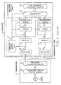
- a protection channel monitoring system according to an embodiment of the present invention comprises a transmitter 31 and a receiver 32 interconnected by transmission line 13 of a protection channel.
- the system has circuit portions similar to those of the known system of Fig. 1.
- the similar circuit portions are designated by the same reference characters as in Fig. 1.
- the transmitter 31 comprises a check signal generator 33 and a unipolar/bipolar converter 16.
- the check signal generator 33 is for generating a checking signal for monitoring the protection channel.
- the check signal generator 33 comprises a 1/N (N being an integer larger than 1) divider 34 for dividing the clock pulse signals a of the frequency (f) from the clock pulse generator 14 into a pulse signal a ' of a frequency of (f/N).
- the frequency-divided pulse signal a ' is applied to the pseudo random signal generator 15. Therefore, pseudo random signal generator 15 is driven by the pulse signal a ' of the frequency (f/N) and produces a pseudo random signal b.
- the pseudo random signal b comprises logical "1" level portions and "0" levels portions sequentially arranged at random.
- the pseudo random signal b has a repetition period of M longer than the period L (M>L) of the pseudo random signal b in Fig. 1.
- the clock pulse signal a , the frequency-divided pulse signal a ', and the pseudo random signal b are applied to an N-bit pattern converter 35.
- N-bit pattern convertor 35 converts each of the N-bit length logical "0" level portions and each of the N-bit length logical “1" level portions into a first predetermined N-bit code pattern comprising logical "0" level and "1” level bits and a second predetermined N-bit code pattern comprising logical "0" level and "1” level bits, respectively, under control of the clock pulse signal a and the frequency divided pulse signal a '.
- Fig. 4 shows examples of the first predetermined N-bit code pattern and the second N-bit code pattern for various values of N.
- N is an integer of 3 or more
- the first predetermined N-bit code pattern is formed so that the logical "0" level bits are disposed to continue by two bits while the logical "1" level bits being disposed at intervals.
- the second predetermined N-bit code pattern is formed so that the logical "1" level bits are disposed to continue by two bits while the logical "0" level bits being at intervals.
- N-bit pattern convertor 35 produces a pattern converted signal as the unipolar check signal.
- the unipolar check signal is applied to unipolar/bipolar convertor 16 and is converted into the AMI code signal.
- the AMI code signal is split into a plurality of AMI code signals c1 - c m which are transmitted to the receiver through the protection channel in the similar manner as in the known system of Fig. 1.
- the receiver 32 comprises m AMI code decoding circuits 37 similar to the m channel AMI code decoding circuits 24 in Fig. 1. Similar circuit portions are represented by the same reference numerals as in Fig. 1.
- the sampling pulse deriving circuit 36 is different from the sampling pulse deriving circuit 19 in Fig. 1 and derives from the RZ signal d1 a timing pulse signal as a sampling pulse signal g' having a frequency of f/N.
- the sampling pulse signal g' is applied to each delay circuit 20 and each phase comparator 21. Therefore, each delay circuit 20 and each phase comparator 21 are driven at N-bit intervals.
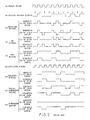
- the 1/3 frequency divider 34 converts the clock pulse signal a into a 1/3 frequency-divided pulse signal a ' ((a') in Fig. 5), which is supplied to the pseudo random signal generator 15 and the N-bit pattern converter 35.
- the pseudo random signal generator 15 generates, in response to the 1/3 frequency divided pulse signal a ', the pseudo random signal b ((b) in Fig. 5), which is fed to the N-bit pattern converter 35.
- the pseudo random signal comprises mark portions "111" each having the logical "1" level for successive three bits and space portions "000” each having the logical "0" level for successive three bits.
- the converted signal b' ((b') in Fig. 5) is applied to the unipolar/bipolar converter 16, as the check signal.
- the check signal b' is converted into an AMI code signal or a bipolar signal c which is split into a plurality of AMI code signals c1 - c m and transmitted to the receiver 32 through the protection channel.
- the received AMI code signals c1 - c m are absolutely converted at the m rectifiers 17 into RZ signals d1 - d m (see (d) in Fig. 5), respectively, which are applied to 1/2 dividers 18, while one (for example, d1) of them being fed to the sampling pulse deriving circuit 36.
- the sampling pulse deriving circuit 36 derives from the input RZ signal d1 a sampling pulse signal g' (see (g') in fig. 5) having a frequency of 1/3 of the clock pulse frequency (f), which is applied to the delay circuits 20, phase comparators 21, and the comparator 22.
- the dividers 18 convert the input RZ signals d1 - d m into divided signals of the NRZ form e1 - e m (see (e) in fig. 5), respectively, which are supplied to delay circuits 20 and phase comparators 21, respectively.
- the delay circuits 20 sample the input divided signals d1 - d m by the sampling pulse signal g' every three bits, respectively, and send out to the phase comparators 21 the delayed signals h1 - h m (see (h) in Fig. 5) which are delayed by 3 bits.
- the phase comparators 21 phase compare the output signals e1 - e m from the dividers 18 with the output signals h1 - h m from the delay circuits 20, respectively, at every three bits, and output phase-compared output signals i1 - i m (see (i) in Fig. 5) as the decoded NRZ code signals, which are applied to the comparator 22.
- the decoded NRZ code signals i1 - i m are signals having a 1/3 rate of the data transfer rate.
- the comparator 22 receives the decoded NRZ code signals i1 - i m and detects coincidence or non-coincidence between respective decoded NRZ code signals to produce a coincidence/non-coincidence signal j (see (j) in Fig. 5) which is fed to the channel condition decision circuit 23 in a similar manner as in the prior art.
- each divided NRZ signal e comprises a three bit code pattern "001". While, for the three bit successive space portion of the check signal b being converted into first three bit code pattern "100”, each divided NRZ signal e comprises a three bit pattern "111" or "000", as shown at (b), (b'), and (I) of (e) in Fig. 5. Each pattern has a constant portion maintained over two successive bits. By sampling the successive two bits constant portion, the timing margin for the sampling can be set to two or three bits.
- the decoded NRZ code signals i1 - i m are equal to one another (see (I) of (i) in Fig. 5) when no error is caused in each of the input AMI code signals c1 - c m transmitted through the protection channel. Therefore, the output signal j from the comparator 22 indicates the coincidence or no code error (see (I) of (j) in Fig. 5). The coincidence signal is sent out to the channel condition decision circuit 23.
- the decoded NRZ signal (see (II) of (i) in Fig. 5) is different from the other decoded NRZ signal (see (I) of (i) in Fig. 5), so that the comparator 22 sends the output signal indicating the non-coincidence or presence of the code error (see (II) of (j) in Fig. 5) to the channel condition decision circuit 23. Thereby, it is possible to monitor the condition of the protection channel.
Landscapes
- Engineering & Computer Science (AREA)
- Computer Networks & Wireless Communication (AREA)
- Signal Processing (AREA)
- Dc Digital Transmission (AREA)
- Detection And Prevention Of Errors In Transmission (AREA)
- Time-Division Multiplex Systems (AREA)
Claims (7)
- Ersatzkanalüberwachungssystem mit einem Sender (31) und einem Empfänger (32), die durch einen Ersatzkanal (c₁ - cm, 13) miteinander gekoppelt sind, zur Verwendung in einem digitalen Kommunikationsnetz, wobei der Sender (31) aufweist: einen Prüfsignalgenerator (33) zum Erzeugen eines Unipolarprüfsignals und einen Unipolar/Bipolar-Wandler (16) zum Umwandeln des Prüfsignals in ein Bipolarsignal, um ein AMI-Codesignal (Bipolarcodesignal) zu erzeugen, wobei das AMI-Codesignal in mehrere AMI-Codesignale aufgeteilt wird, die zum Empfänger über den Ersatzkanal übertragen werden, und der Empfänger (32) aufweist: mehrere Decodierer (37), die auf die über den Ersatzkanal empfangenen AMI-Codesignale reagieren, zum Decodieren der AMI-Codesignale in NRZ-Codesignale (Wechselschrift-Codesignale), um jeweils decodierte NRZ-Signale (i₁ - im) zu erzeugen, einen Komparator (22) zum Vergleichen der decodierten NRZ-Signale, um ein Übereinstimmungs-/Nichtübereinstimmungssignal (j) zu erzeugen, und eine Entscheidungsschaltung (23), die auf das Übereinstimmungs-/Nichtübereinstimmungssignal reagiert, zum Entscheiden über den Zustand des Ersatzkanals, und wobei der Prüfsignalgenerator (33) aufweist:
einen Taktimpulsgenerator (14) zum Erzeugen eines Taktimpulssignals (a) mit einer Taktfrequenz (f), wobei eine Periode (1/f) des Taktimpulssignals die Länge eines Bits definiert;
einen Frequenzteiler (34) mit einem Teilungsverhältnis von 1/N (wobei N gleich 3 oder eine größere ganze Zahl ist) zum Frequenzteilen des Taktimpulssignals, um ein frequenzgeteiltes Impulssignal (a') zu erzeugen;
einen Pseudozufallsgenerator (15), der auf das frequenzgeteilte Impulssignal (a') reagiert, zum Erzeugen eines Pseudozufallssignals (b) mit einer ausreichend langen Wiederholperiode, wobei das Pseudozufallssignal N Bit lange Abschnitte mit dem logischen Pegel "1" und N Bit lange Abschnitte mit dem logischen Pegel "0" aufweist, die in einer Zufallsfolge angeordnet sind; und
einen N-Bit-Musterwandler (35), der auf das Pseudozufallssignal (b) reagiert, zum Umwandeln jedes N Bit langen Abschnitts mit dem logischen Pegel "0" und jedes N Bit langen Abschnitts mit dem logischen Pegel "1" in ein erstes vorbestimmtes N-Bit-Codemuster mit Bits mit dem logischen Pegel "0" und "1" bzw. ein zweites vorbestimmtes N-Bit-Codemuster mit Bits mit dem logischen Pegel "0" und "1", wobei der N-Bit-Musterwandler (35) ein musterumgewandeltes Signal als das Unipolarprüfsignal erzeugt, N gleich 3 oder eine größere ganze Zahl ist und wobei das erste vorbestimmte N-Bit-Codemuster gebildet wird, indem die Bits mit dem logischen Pegel "0" so angeordnet werden, daß sie sich über zwei Bits fortsetzen, während die Bits mit dem logischen Pegel "1" dazwischen angeordnet werden, und das zweite vorbestimmte N-Bit-Codemuster gebildet wird, indem die Bits mit dem logischen Pegel "1" so angeordnet werden, daß sie sich über zwei Bits fortsetzen, während die Bits mit dem logischen Pegel "0" dazwischen angeordnet werden. - Ersatzkanalüberwachungssystem nach Anspruch 1, wobei der Empfänger (32) eine Ableitungsschaltung (36) für Abtastimpulse zum Ableiten eines Zeitsteuersignals aus einem der empfangenen AMI-Codesignale (c₁ - cm) aufweist, das synchron zu dem frequenzgeteilten Impulssignal (a') ist, und wobei das Zeitsteuersignal als Abtastimpulssignal (g') beim Decodieren durch jeden Decodierer (37) vorgesehen ist.
- Ersatzkanalüberwachungssystem nach Anspruch 2, wobei jeder Decodierer (37) aufweist: einen Gleichrichter (17) zum Gleichrichten eines entsprechenden der empfangenen AMI-Codesignale (c₁ - cm), um ein RZ-Signal (Rückkehrnach-Null-Signal) zu erzeugen, einen Teiler (18) zum Teilen des RZ-Signals durch 2, um ein 1/2-geteiltes Signal (e₁ - em) in NRZ-Form zu erzeugen, eine Verzögerungsschaltung (20), die auf das Abtastimpulssignal (g') reagiert, zum Verzögern des 1/2-geteilten Signals um N Bits, um ein verzögertes Signal (h₁ - hm) zu erzeugen, einen Phasenkomparator (21), der auf das Abtastimpulssignal (g') reagiert, zum Vergleichen des verzögerten Signals (h₁ - hm) in der Phase mit dem 1/2-geteilten Signal (e₁ - em), um eine Ausgabe (i₁ - im) als das decodierte NRZ-Signal zu erzeugen.
- Ersatzkanalüberwachungssystem nach Anspruch 3, wobei die Ableitungsschaltung für Abtastimpulse mit dem Gleichrichter eines der Decodierer gekoppelt ist und die Ableitungsschaltung für Abtastimpulse das Abtastimpulssignal aus dem RZ-Signal von dem Gleichrichter ableitet.
- Sender zur Verwendung in einem Überwachungssystem zum Überwachen eines Ersatzkanals in einem digitalen Kommunikationsnetz, wobei der Sender aufweist:
einen Prüfsignalgenerator (33) zum Erzeugen eines Unipolarprüfsignals, wobei der Prüfsignalgenerator (33) aufweist:
einen Taktimpulsgenerator (14) zum Erzeugen eines Taktimpulssignals (a) mit einer Taktfrequenz (f), wobei eine Periode (1/f) des Taktimpulssignals die Länge eines Bits definiert;
einen Frequenzteiler (34) mit einem Teilungsverhältnis von 1/N (wobei N gleich 3 oder eine größere ganze Zahl ist) zum Frequenzteilen des Taktimpulssignals, um ein frequenzgeteiltes Impulssignal (a') zu erzeugen;
einen Pseudozufallssignalgenerator (15), der auf das frequenzgeteilte Impulssignal (a') reagiert, zum Erzeugen eines Pseudozufallssignals (b) mit einer ausreichend langen Wiederholperiode, wobei das Pseudozufallssignal (b) N Bit lange Abschnitte mit dem logischen Pegel "1" und N Bit lange Abschnitte mit dem logischen Pegel "0" aufweist, die in einer Zufallsfolge angeordnet sind; und
einen N-Bit-Musterwandler (35), der auf das Pseudozufallssignal (b) reagiert, zum Umwandeln jedes N Bit langen Abschnitts mit dem logischen Pegel "0" und jedes N Bit langen Abschnitts mit dem logischen Pegel "1" in ein erstes vorbestimmtes N-Bit-Codemuster mit Bits mit dem logischen Pegel "0" und "1" bzw. in ein zweites vorbestimmtes N-Bit-Codemuster mit Bits mit dem logischen Pegel "0" und "1", wobei der N-Bit-Musterwandler (35) ein musterumgewandeltes Signal als das Unipolarprüfsignal erzeugt; und
einen Unipolar/Bipolar-Wandler (16) zum Umwandeln des Prüfsignals in ein Bipolarsignal, um ein AMI-Codesignal (Bipolarcodesignal) zu erzeugen, wobei das AMI-Codesignal in mehrere AMI-Codesignale aufgeteilt wird, die aufgeteilten AMI-Codesignale zu einem Empfänger (32) über den Ersatzkanal übertragen werden,
wobei N gleich 3 oder eine größere ganze Zahl ist und das erste vorbestimmte N-Bit-Codemuster gebildet wird, indem die Bits mit dem logischen Pegel "0" so angeordnet werden, daß sie sich über zwei Bits fortsetzen, während die Bits mit dem logischen Pegel "1" dazwischen angeordnet werden, und das zweite vorbestimmte N-Bit-Codemuster gebildet wird, indem die Bits mit dem logischen Pegel "1" so angeordnet werden, daß sie sich über zwei Bits fortsetzen, während die Bits mit dem logischen Pegel "0" dazwischen angeordnet werden. - Empfänger zur Verwendung in einem Überwachungssystem zum Überwachen eines Ersatzkanals und zur kombinierten Verwendung mit einem Sender nach Anspruch 5, wobei der Empfänger (32) aufweist:
eine Ableitungsschaltung (36) für Abtastimpulse zum Ableiten eines Zeitsteuersignals aus einem der über den Ersatzkanal empfangenen AMI-Codesignale (c₁ - cm), das synchron zu dem im Sender erzeugten frequenzgeteilten Impulssignal (a') ist, wobei das Zeitsteuersignal als ein Abtastimpulssignal (g') vorgesehen ist;
mehrere Decodierer (37) zum Decodieren der AMI-Codesignale in NRZ-Codesignale (Wechselschrift-Codesignale), um jeweils decodierte NRZ-Signale zu erzeugen, wobei jeder Decodierer (37) aufweist:
einen Gleichrichter (17) zum Gleichrichten eines entsprechenden der empfangenen AMI-Codesignale (c₁ - cm), um ein RZ-Signal (Rückkehr-nach-Null-Signal) zu erzeugen;
einen Teiler (18) zum Teilen des RZ-Signals durch 2, um ein 1/2-geteiltes Signal (e₁ - em) in NRZ-Form zu erzeugen;
eine Verzögerungsschaltung (20), die auf das Abtastimpulssignal (g') reagiert, zum Verzögern des 1/2-geteilten Signals um N Bits, um ein verzögertes Signal (h₁ - hm) zu erzeugen; und
einen Phasenkomparator (21), der auf das Abtastimpulssignal (g') reagiert, zum Vergleichen des verzögerten Signals (h₁ - hm) in der Phase mit dem 1/2-geteilten Signal (e₁ - em), um eine Ausgabe (i₁ - im) als das decodierte NRZ-Signal zu erzeugen; und
einen Komparator (22) zum Vergleichen der decodierten NRZ-Signale, um ein Übereinstimmungs-/Nichtübereinstimmungssignal (j) zu erzeugen; und
eine Entscheidungsschaltung (23), die auf das Übereinstimmungs-/Nichtübereinstimmungssignal (j) reagiert, zum Entscheiden über den Zustand des Ersatzkanals. - Empfänger nach Anspruch 6, wobei die Ableitungsschaltung (36) für Abtastimpulse mit dem Gleichrichter (17) eines der Decodierer (37) gekoppelt ist und wobei die Ableitungsschaltung (36) für Abtastimpulse das Abtastimpulssignal aus dem RZ-Signal von dem Gleichrichter (17) ableitet.
Applications Claiming Priority (2)
| Application Number | Priority Date | Filing Date | Title |
|---|---|---|---|
| JP61099254A JPH0624345B2 (ja) | 1986-04-28 | 1986-04-28 | 予備回線監視回路 |
| JP99254/86 | 1986-04-28 |
Publications (3)
| Publication Number | Publication Date |
|---|---|
| EP0243938A2 EP0243938A2 (de) | 1987-11-04 |
| EP0243938A3 EP0243938A3 (en) | 1990-01-31 |
| EP0243938B1 true EP0243938B1 (de) | 1993-09-29 |
Family
ID=14242575
Family Applications (1)
| Application Number | Title | Priority Date | Filing Date |
|---|---|---|---|
| EP87106155A Expired - Lifetime EP0243938B1 (de) | 1986-04-28 | 1987-04-28 | Ersatzkanalüberwachungssystem unter Verwendung eines Prüfsignals mit zwei verschiedenen, in einer Zufallsfolge angeordneten n-Bit-Kodemustern |
Country Status (6)
| Country | Link |
|---|---|
| US (1) | US4811359A (de) |
| EP (1) | EP0243938B1 (de) |
| JP (1) | JPH0624345B2 (de) |
| AU (1) | AU587754B2 (de) |
| CA (1) | CA1274292A (de) |
| DE (1) | DE3787561D1 (de) |
Families Citing this family (11)
| Publication number | Priority date | Publication date | Assignee | Title |
|---|---|---|---|---|
| AU618289B2 (en) * | 1987-11-10 | 1991-12-19 | Nec Corporation | Channel switching system |
| JPH01128631A (ja) * | 1987-11-13 | 1989-05-22 | Nec Corp | デジタル多重化装置のモニター方式 |
| JP2524371B2 (ja) * | 1987-12-17 | 1996-08-14 | 日本電気株式会社 | 予備回線監視回路 |
| JPH01198834A (ja) * | 1988-02-03 | 1989-08-10 | Fujitsu Ltd | 回線切替装置 |
| US5058129A (en) * | 1989-10-11 | 1991-10-15 | Integrated Network Corporation | Two-wire digital transmission loop |
| NL9002176A (nl) * | 1990-10-08 | 1992-05-06 | Philips Nv | Werkwijze voor het verminderen van deeltjescontaminatie tijdens sputteren en een sputterinrichting voor gebruik van een dergelijke werkwijze. |
| US5283807A (en) * | 1992-10-21 | 1994-02-01 | Tutankhamon Electronics, Inc. | EMI suppression coding |
| US5757652A (en) * | 1995-12-21 | 1998-05-26 | Tektronix, Inc. | Electrical signal jitter and wander measurement system and method |
| US6029058A (en) * | 1996-07-19 | 2000-02-22 | The Board Of Trustee Of The Leland Stanford Junior University | Spectrum control for direct conversion radio frequency reception |
| US5754437A (en) * | 1996-09-10 | 1998-05-19 | Tektronix, Inc. | Phase measurement apparatus and method |
| DE10229860A1 (de) * | 2002-07-03 | 2004-01-29 | Infineon Technologies Ag | Verfahren und Sendevorrichtung zum Übertragen eines zweiwertigen Signals |
Family Cites Families (7)
| Publication number | Priority date | Publication date | Assignee | Title |
|---|---|---|---|---|
| US4395772A (en) * | 1981-04-30 | 1983-07-26 | Bell Telephone Laboratories, Incorporated | Line protection switch controller |
| US4417348A (en) * | 1981-04-30 | 1983-11-22 | Bell Telephone Laboratories, Incorporated | Errorless line protection switcher |
| JPS58134545A (ja) * | 1982-02-04 | 1983-08-10 | Nec Corp | サ−ビスチヤンネル信号伝送方式 |
| EP0142138B1 (de) * | 1983-11-11 | 1988-10-26 | Fujitsu Limited | System zur Reservenumschaltung für eine Trägerübertragungsleitung |
| JPS60208134A (ja) * | 1984-04-02 | 1985-10-19 | Nec Corp | 無線通信方式 |
| US4577312A (en) * | 1984-07-05 | 1986-03-18 | At&T Bell Laboratories | Arrangement for wideband transmission via a switched network |
| US4598399A (en) * | 1984-11-20 | 1986-07-01 | Rockwell International Corporation | Multichannel multisite signal protection channel switching apparatus |
-
1986
- 1986-04-28 JP JP61099254A patent/JPH0624345B2/ja not_active Expired - Lifetime
-
1987
- 1987-04-28 DE DE87106155T patent/DE3787561D1/de not_active Expired - Lifetime
- 1987-04-28 US US07/043,653 patent/US4811359A/en not_active Expired - Lifetime
- 1987-04-28 EP EP87106155A patent/EP0243938B1/de not_active Expired - Lifetime
- 1987-04-28 AU AU72150/87A patent/AU587754B2/en not_active Ceased
- 1987-04-28 CA CA000535734A patent/CA1274292A/en not_active Expired
Also Published As
| Publication number | Publication date |
|---|---|
| EP0243938A2 (de) | 1987-11-04 |
| JPS62254541A (ja) | 1987-11-06 |
| AU587754B2 (en) | 1989-08-24 |
| CA1274292A (en) | 1990-09-18 |
| AU7215087A (en) | 1987-10-29 |
| DE3787561D1 (de) | 1993-11-04 |
| JPH0624345B2 (ja) | 1994-03-30 |
| US4811359A (en) | 1989-03-07 |
| EP0243938A3 (en) | 1990-01-31 |
Similar Documents
| Publication | Publication Date | Title |
|---|---|---|
| US4004100A (en) | Group frame synchronization system | |
| US4475208A (en) | Wired spread spectrum data communication system | |
| US5408473A (en) | Method and apparatus for transmission of communication signals over two parallel channels | |
| EP0667695A1 (de) | Funkinformations- und kommunikationssystem mit einem mehrträger-spreizspektrum-übertragungssystem | |
| EP0244629B1 (de) | Funkübertragungssystem mit vereinfachter Fehlerkorrekturschaltung und schneller Kanalumschaltung | |
| CA1212161A (en) | Ring communications system | |
| US4811359A (en) | Protection channel monitoring system using a check signal comprising two different N-bit code patterns sequentially arranged at random | |
| CA1288520C (en) | Synchronization recovery in a communications system | |
| US7333518B2 (en) | Transmission method and transmission system as well as communications device | |
| US3809817A (en) | Asynchronous quadriphase communications system and method | |
| CA1312362C (en) | Fault detection signal transmission system | |
| EP0137225B1 (de) | Bidirektionales Übertragungssystem aus einem Zweidrahtbus mit aktivem Abschluss | |
| US4232387A (en) | Data-transmission system using binary split-phase code | |
| US4773081A (en) | Channel switching system | |
| EP0320968B1 (de) | Schaltung zur Überwachung eines Ersatzkanals | |
| US6421393B1 (en) | Technique to transfer multiple data streams over a wire or wireless medium | |
| US4213007A (en) | Method and apparatus for monitoring a pulse-code modulated data transmission | |
| US3548309A (en) | Data rate converter | |
| EP0208558B1 (de) | Übertragungssystem für CMI-Signale | |
| WO1987006412A1 (en) | Encoding and decoding signals for transmission over a multi-access medium | |
| CA2088210A1 (en) | Procedure for synchronizing circuit elements of a telecommunications system | |
| US5222102A (en) | Digital phased locked loop apparatus for bipolar transmission systems | |
| EP0476968A2 (de) | Taktrückgewinnungssystem | |
| JP3646594B2 (ja) | 通信システム | |
| Schneider et al. | A N+ 2 protection switching system for synchronous STM-1 signals and plesiochronous 140 Mbit/s signals by using two carrier technique |
Legal Events
| Date | Code | Title | Description |
|---|---|---|---|
| PUAI | Public reference made under article 153(3) epc to a published international application that has entered the european phase |
Free format text: ORIGINAL CODE: 0009012 |
|
| 17P | Request for examination filed |
Effective date: 19870430 |
|
| AK | Designated contracting states |
Kind code of ref document: A2 Designated state(s): DE FR GB IT SE |
|
| PUAL | Search report despatched |
Free format text: ORIGINAL CODE: 0009013 |
|
| AK | Designated contracting states |
Kind code of ref document: A3 Designated state(s): DE FR GB IT SE |
|
| 17Q | First examination report despatched |
Effective date: 19920113 |
|
| GRAA | (expected) grant |
Free format text: ORIGINAL CODE: 0009210 |
|
| AK | Designated contracting states |
Kind code of ref document: B1 Designated state(s): DE FR GB IT SE |
|
| PG25 | Lapsed in a contracting state [announced via postgrant information from national office to epo] |
Ref country code: IT Free format text: LAPSE BECAUSE OF FAILURE TO SUBMIT A TRANSLATION OF THE DESCRIPTION OR TO PAY THE FEE WITHIN THE PRE;WARNING: LAPSES OF ITALIAN PATENTS WITH EFFECTIVE DATE BEFORE 2007 MAY HAVE OCCURRED AT ANY TIME BEFORE 2007. THE CORRECT EFFECTIVE DATE MAY BE DIFFERENT FROM THE ONE RECORDED.SCRIBED TIME-LIMIT Effective date: 19930929 Ref country code: FR Effective date: 19930929 Ref country code: DE Effective date: 19930929 |
|
| REF | Corresponds to: |
Ref document number: 3787561 Country of ref document: DE Date of ref document: 19931104 |
|
| EN | Fr: translation not filed | ||
| PLBE | No opposition filed within time limit |
Free format text: ORIGINAL CODE: 0009261 |
|
| STAA | Information on the status of an ep patent application or granted ep patent |
Free format text: STATUS: NO OPPOSITION FILED WITHIN TIME LIMIT |
|
| 26N | No opposition filed | ||
| EAL | Se: european patent in force in sweden |
Ref document number: 87106155.2 |
|
| PGFP | Annual fee paid to national office [announced via postgrant information from national office to epo] |
Ref country code: GB Payment date: 19960423 Year of fee payment: 10 |
|
| PG25 | Lapsed in a contracting state [announced via postgrant information from national office to epo] |
Ref country code: GB Effective date: 19970428 |
|
| GBPC | Gb: european patent ceased through non-payment of renewal fee |
Effective date: 19970428 |
|
| PGFP | Annual fee paid to national office [announced via postgrant information from national office to epo] |
Ref country code: SE Payment date: 20020417 Year of fee payment: 16 |
|
| PG25 | Lapsed in a contracting state [announced via postgrant information from national office to epo] |
Ref country code: SE Free format text: LAPSE BECAUSE OF NON-PAYMENT OF DUE FEES Effective date: 20030429 |
|
| EUG | Se: european patent has lapsed |