EP0243733A2 - Verfahren zur Regelung eines Einseitenband-Aufwärtsmischers sowie Anordnung hierzu - Google Patents
Verfahren zur Regelung eines Einseitenband-Aufwärtsmischers sowie Anordnung hierzu Download PDFInfo
- Publication number
- EP0243733A2 EP0243733A2 EP87105025A EP87105025A EP0243733A2 EP 0243733 A2 EP0243733 A2 EP 0243733A2 EP 87105025 A EP87105025 A EP 87105025A EP 87105025 A EP87105025 A EP 87105025A EP 0243733 A2 EP0243733 A2 EP 0243733A2
- Authority
- EP
- European Patent Office
- Prior art keywords
- mixer
- intermediate frequency
- frequency
- sideband
- oscillator
- Prior art date
- Legal status (The legal status is an assumption and is not a legal conclusion. Google has not performed a legal analysis and makes no representation as to the accuracy of the status listed.)
- Granted
Links
Images


Classifications
-
- H—ELECTRICITY
- H03—ELECTRONIC CIRCUITRY
- H03G—CONTROL OF AMPLIFICATION
- H03G3/00—Gain control in amplifiers or frequency changers
- H03G3/20—Automatic control
- H03G3/30—Automatic control in amplifiers having semiconductor devices
- H03G3/3036—Automatic control in amplifiers having semiconductor devices in high-frequency amplifiers or in frequency-changers
- H03G3/3042—Automatic control in amplifiers having semiconductor devices in high-frequency amplifiers or in frequency-changers in modulators, frequency-changers, transmitters or power amplifiers
-
- H—ELECTRICITY
- H03—ELECTRONIC CIRCUITRY
- H03D—DEMODULATION OR TRANSFERENCE OF MODULATION FROM ONE CARRIER TO ANOTHER
- H03D7/00—Transference of modulation from one carrier to another, e.g. frequency-changing
-
- H—ELECTRICITY
- H03—ELECTRONIC CIRCUITRY
- H03D—DEMODULATION OR TRANSFERENCE OF MODULATION FROM ONE CARRIER TO ANOTHER
- H03D7/00—Transference of modulation from one carrier to another, e.g. frequency-changing
- H03D7/16—Multiple-frequency-changing
- H03D7/165—Multiple-frequency-changing at least two frequency changers being located in different paths, e.g. in two paths with carriers in quadrature
-
- H—ELECTRICITY
- H03—ELECTRONIC CIRCUITRY
- H03D—DEMODULATION OR TRANSFERENCE OF MODULATION FROM ONE CARRIER TO ANOTHER
- H03D2200/00—Indexing scheme relating to details of demodulation or transference of modulation from one carrier to another covered by H03D
- H03D2200/0001—Circuit elements of demodulators
- H03D2200/0025—Gain control circuits
-
- H—ELECTRICITY
- H03—ELECTRONIC CIRCUITRY
- H03D—DEMODULATION OR TRANSFERENCE OF MODULATION FROM ONE CARRIER TO ANOTHER
- H03D2200/00—Indexing scheme relating to details of demodulation or transference of modulation from one carrier to another covered by H03D
- H03D2200/0001—Circuit elements of demodulators
- H03D2200/0029—Loop circuits with controlled phase shift
-
- H—ELECTRICITY
- H03—ELECTRONIC CIRCUITRY
- H03D—DEMODULATION OR TRANSFERENCE OF MODULATION FROM ONE CARRIER TO ANOTHER
- H03D2200/00—Indexing scheme relating to details of demodulation or transference of modulation from one carrier to another covered by H03D
- H03D2200/0041—Functional aspects of demodulators
- H03D2200/0094—Measures to address temperature induced variations of demodulation
- H03D2200/0096—Measures to address temperature induced variations of demodulation by stabilising the temperature
-
- H—ELECTRICITY
- H03—ELECTRONIC CIRCUITRY
- H03D—DEMODULATION OR TRANSFERENCE OF MODULATION FROM ONE CARRIER TO ANOTHER
- H03D7/00—Transference of modulation from one carrier to another, e.g. frequency-changing
- H03D7/14—Balanced arrangements
- H03D7/1408—Balanced arrangements with diodes
-
- H—ELECTRICITY
- H03—ELECTRONIC CIRCUITRY
- H03D—DEMODULATION OR TRANSFERENCE OF MODULATION FROM ONE CARRIER TO ANOTHER
- H03D7/00—Transference of modulation from one carrier to another, e.g. frequency-changing
- H03D7/18—Modifications of frequency-changers for eliminating image frequencies
Definitions
- the invention relates to a method for controlling a single-sideband upward mixer according to the preamble of claim 1 and an arrangement therefor.
- the object of the invention is to provide a method which enables good interference line suppression with broadband tunability over frequency and also changes such as those e.g. due to aging, frequency response, temperature and level changes.
- An arrangement for carrying out this method is also to be specified.
- Claim 5 relates to an arrangement for performing the method.
- the invention enables the regulation of changes - aging, frequency response, temperature and level changes - with high interference line suppression and broadband tunability.
- the single-sideband mixer according to EP 119 439 A2 there is oscillator suppression and broadband tunability, but the image frequency suppression is not sufficiently large and changes such as are e.g. due to aging, frequency response, temperature and level changes cannot be recorded.
- a standard single-sideband mixer with a downstream sideband filter no frequency change is possible without changing the filter.
- Such a sideband filter also has to meet very high requirements with regard to frequency response and transit time.
- the interference line suppression can be set and optimized for a fixed operating frequency, but said changes cannot be taken into account. A new setting and optimization must be carried out for each frequency change.
- the oscillator suppression and the undesired sideband (image frequency) can be below a certain value, e.g. -35 to -40 dB, regulate.
- the advantage of the invention lies in the use of the radio frequency signal as the oscillator frequency for back-mixing the interference signals, in contrast to the use of the oscillator signal for the mixing stages in a conventional mixer, for example according to DE 33 44 318 A1.
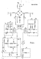
- the basic circuit diagram of the single-sideband up-mixer according to the invention is shown in FIG. 1.
- the intermediate frequency circuit of this up-mixer consists of two mixing stages (balanced mixers) M1 and M2.
- the frequency IF to be converted is led to one of the mixing stages M1 and M2 via the 3 dB / 90 ° coupler C3, in each case via an attenuator Dg, Dg 'and a phase shifter Ph, Ph'.
- the preselectable oscillator frequency L0 is led to the two mixing stages M1 and M2 via the signal branching C1.
- the outputs of the mixer stages M1 and M2 are connected to the 3 dB / 90 ° coupler C2, at one output of which the radio frequency RF '- mixer output signal - can be removed.
- a small part of the radio frequency RF ' is coupled out via the coupler C4.
- the decoupled radio frequency RF ' is amplified in an amplifier stage V1 if necessary.
- the possibly amplified signal controls a back mixer M3.
- the radio frequency RF 'thus serves as an oscillator frequency for the back mixer M3, which is designed as a single-ended mixer.
- the undesired interference signals (undesired sideband; oscillator frequency LO for the two mixer stages M1 and M2) are converted into the intermediate frequency position by means of the back mixer M3.
- the output signal of the back mixer M3 reaches a filter F1 for the via a diplexer DP Intermediate frequency IF and a filter F2 for the 1st harmonic, ie twice the intermediate frequency 2xIF.
- These filtered signals are rectified by means of rectifiers G1 and G2, possibly amplified and integrated by means of integration elements IG1 and IG2.
- the voltages V R1 and V R2 at the outputs are a measure of the oscillator suppression and sideband suppression of the mixer.
- the voltages V R1 and V R2 are fed to a microcomputer MC with interface circuits (Fig.
- control signals V B1 and V B2 for the mixing stages M1 and M2 as well as control signals V a and Vy for a controllable attenuator Dg and a controllable phase shifter To generate Ph.
- the controllable attenuator Dg and the controllable phase shifter Ph are located in the intermediate frequency branch between coupler C3 and mixer M1, whereas in the branch between coupler C3 and mixer M2 a fixed attenuator Dg 'and a fixed phase shifter Ph' are arranged, the control signals V B1 and V B2 are supplied to the mixer diodes of the mixer stages M1 and M2 (FIG. 5) as DC control voltages for suppressing the oscillator frequency LO.
- control signals V ⁇ and V a are used to adjust the phase of the phase shifter Ph and to adjust the damping of the attenuator Dg.
- the exact structure of these modules is described in connection with FIG. 4.
- an electronic tunability of the phase shifter Ph of + 20 ° is required and an electronic tunability of the attenuator Dg of + 1.5 dB.
- the basic structure of the microcomputer with interface circuits is shown in FIG. 2.
- the voltages V R1 and V R2 from the back mixer are supplied to A / D converters AD1 and AD2, respectively.
- a / D converter for example, the integrated ADC 0804 can be used.
- the A / D converted signals are fed to the bus of a microcomputer.
- An 8748 from Intel is suitable as a microcomputer.
- the signal processing in this microcomputer takes place according to the flow chart in FIG. 3. First, start values V B1 , V B2 , V a and V ⁇ are specified. These are chosen so that the corresponding control voltages with respect to V B1 and V B2 are 0. Other starting values are specified for V and V ⁇ .
- a threshold value S is assumed to be -35 to -40 dB.
- a ⁇ value ( ⁇ V B1 , ⁇ V B2 , ⁇ V a , ⁇ V ⁇ ) is always added or subtracted and compared again to determine a new calculated value. With a stock of values of, for example, 256 binary stages, these ⁇ values can just correspond to one binary stage. If the comparison in a corresponding decision loop of the flow chart no longer yields a deviation, the last calculated value is passed on to an I / O port as an 8-bit wide word.
- the 8255A blocks from Intel can be used for the I / O ports.
- D / A converters DA1 to DA4 are connected to the I / O ports.
- the control voltages V B1 , VB2, V a , V ⁇ can be tapped via any operational amplifiers required, for example 4741.
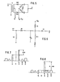
- the circuit diagram of the intermediate frequency circuit is shown in Fig. 4.
- the intermediate frequency IF is conducted via a DC isolating capacitor Ct1 to a diode bridge PD consisting of 4 pin diodes.
- One branch of the pin-diode bridge PD can be switched via an input 1 or 2.
- input 1 By controlling input 1 with a positive potential or input 2 with a negative potential, the selection of the sideband to be suppressed (LSB / USB) is possible.
- the two outputs of the pin-diode bridge PD are connected to the inputs via coupling capacitors Ck of the 3 dB / 90 ° coupler C3 connected. The two outputs of this coupler each lead to one of the phase shifters Ph, Ph '.
- the phase shifter Ph can be adjusted in its phase by the control signal V ⁇ , whereas the phase shifter Ph 'is fixed by the voltage VDC.
- the phase shifter Ph is controlled by changing the bias of the two capacitance diodes CD1 and CD2 as a function of the control voltage V I via the resistors R1 and R2.
- the phase shifter Ph ' has the same structure.
- the controllable attenuator Dg consists of a transistor stage Ts, the base of which is supplied with the control signal Va.
- a diode D1 is located in the longitudinal branch of the controllable attenuator Dg, ie between the output of the controllable phase shifter Ph and the input of the mixing stage M1.
- the anode and cathode of this diode D1 are each connected via an RC element and a further diode to the collector of the transistor stage Ts and to a DC supply voltage V DC .
- the emitter of transistor stage Ts is connected to the anode of diode D1 via RF blocking elements Cb, Lb.
- the fixed attenuator Dg 'between phase shifter Ph' and mixer M2 consists of a resistance T-element.
- an adjustable delay element LZ is connected upstream of this T element.
- the intermediate-q uenzsi g dimensional IF1 and IF2 are out out for driving the mixer stages M1 and M2 available at the outputs 3 and 4.
- the structure of the mixing stages M1 and M2 is shown in Fig. 5.
- the oscillator frequency LO is fed in on the primary side of a transformer Ü.
- the winding ends of the secondary winding of the transformer U are connected to the mixer diodes DM1 and DM2 and that the one end with one Cathode and the other end with an anode of a mixer diode.
- the ends of the mixer diodes facing away from the transformer U are connected to one another via DC voltage isolating capacitors.
- the frequency to be converted IF - IF1 out , IF2 out - is fed in at this connection point.
- the DC control voltage V B1 or V B2 is supplied to each mixer stage via a triangular resistor circuit.
- Two corners of the delta circuit are each connected to the connection points between the mixer diodes DM1 and DM2 and the DC isolating capacitors.
- the DC control voltage V B1 or V B2 is supplied at the third corner of the delta connection.
- the radio frequency RF ' can be picked up at the center tap of the secondary winding of the transformer 0.
- High barrier silicon Schottky diodes are preferably suitable as mixer diodes. For each push-pull mixer, one diode is biased by the control voltage V B1 or V B2 so far that a current of 0 to max. 3 mA flows.
- a single-stroke mixer is used as the back mixer M3, which expediently consists of half a mixer stage M1 or M2. It is constructed with only one backmixing diode DR.
- the radio frequency RF ' is fed directly to the anode of the mixing diode.
- the choke Dr1 on the radio frequency side represents an open circuit for the radio frequency RF '.
- the choke Dr2 blocks IF voltage in the direct current path.
- the capacitor C1 represents a short circuit for the radio frequency.
- a fixed bias for the backmixing diode DR is supplied via the resistor R3.
- FIG. 7 shows the output signal spectrum of a conventional QAM modulated single-sideband mixer.
- the desired sideband LO + IF protrudes only slightly above the level of the undesired oscillator frequency L0.
- the unwanted sideband LO-IF is cut by 20 dB.
- FIG. 8 shows the output signal spectrum of a QAM modulated single sideband mixer according to the invention.
- the unwanted sidebands LO-IF, LO + ZIF, ... are reduced by 35 to 40 dB compared to the desired sideband LO + IF.
- a broadband tunability of the mixer over the frequency is given; to do this, only change the oscillator frequency LO without any filter or loop retuning. Changes via temperature, aging, level changes and frequency response are corrected.
- the microcomputer replaces a complex analog control system. The required signal-to-noise ratios of 20 dB for 16 QAM, 28 dB for 64 QAM and 36 dB for 256 QAM are met or exceeded by far.
Landscapes
- Engineering & Computer Science (AREA)
- Power Engineering (AREA)
- Transmitters (AREA)
- Superheterodyne Receivers (AREA)
- Dc-Dc Converters (AREA)
- Amplitude Modulation (AREA)
- Radar Systems Or Details Thereof (AREA)
Abstract
Description
- Die Erfindung betrifft ein Verfahren zur Regelung eines Einseitenband-Aufwärtsmischers gemäß dem Oberbegriff des Patentanspruchs 1 sowie eine Anordnung hierzu.
- Bei Einseitenband-Aufwärtsmischern ist oft eine hohe Störlinienunterdrückung gefordert, insbesondere bei Funkgeräten, die höherwertige digitale Modulationsarten verwenden, wie z.B. 64 QAM (Quadraturamplitudenmodulation) und 256 QAM. Früher wurde das unerwünschte Seitenbandsignal durch einen auf den RF-Kanal abgestimmten mehrkreisigen Bandpaß ausgesiebt (ANT Nachrichtentechnische Berichte, Heft 2, Dezember 1985, Seite 27). Dies ist heutzutage durch die Verwendung von Einseitenbandmischern mit Steuerung der Oszillatorunterdrückung über PROMs und D/A-Wandler (ANT Nachrichtentechnische Berichte, Heft 2, Dezember 1985, Seiten 27 bis 29; EP 119 439 A2) nicht mehr erforderlich.
- Aufgabe der Erfindung ist es ausgehend vom Oberbegriff des Patentanspruchs 1 ein Verfahren anzugeben, welches eine gute Störlinienunterdrückung bei breitbandiger Durchstimmbarkeit über der Frequenz ermöglicht und außerdem Änderungen, wie sie z.B. durch Alterung, Frequenzgang, Temperatur und Pegeländerungen auftreten, ausgleichen kann. Außerdem soll eine Anordnung zum Durchführen dieses Verfahrens angegeben werden.
- Diese Aufgabe wird bezüglich des Verfahrens durch die kennzeichnenden Merkmale des Patentanspruchs 1 gelöst. In den Ansprüchen 1 bis 4 sind vorteilhafte Weiterbildungen des Verfahrens aufgezeigt. Anspruch 5 betrifft eine Anordnung zum Durchführen des Verfahrens.
- Die Erfindung ermöglicht die Ausregelung von Änderungen - Alterung, Frequenzgang, Temperatur und Pegeländerungen - bei gleichzeitig hoher Störlinienunterdrückung und breitbandiger Durchstimmbarkeit. Bei dem Einseitenbandmischer gemäß EP 119 439 A2 ist zwar eine Oszillatorunterdrückung und eine breitbandige Durchstimmbarkeit gegeben, jedoch ist die Spiegelfrequenzunterdrückung nicht hinreichend groß und Änderungen, wie sie z.B. durch Alterung, Frequenzgang, Temperatur und Pegeländerungen auftreten, können nicht erfaßt werden. Bei einem Standard-Einseitenbandmischer mit nachgeschaltetem Seitenbandfilter ist kein Frequenzwechsel ohne Filtertausch möglich. An ein solches Seitenbandfilter sind außerdem sehr hohe Anforderungen bezüglich Frequenzgang und Laufzeit zu stellen. Bei einem herkömmlichen Einseitenbandmischer läßt sich die Störlinienunterdrückung zwar für eine feste Betriebsfrequenz einstellen und optimieren, jedoch können besagte Änderungen nicht berücksichtigt werden. Für jeden Frequenzwechsel muß eine erneute Einstellung und Optimierung vorgenommen werden.
- Aufgrund der erfindungsgemäßen Rückmischung des Mischerausgangssignals läßt sich die Oszillatorunterdrückung und das unerwünschte Seitenband (Spiegelfrequenz) unter einen bestimmten Wert, z.B. -35 bis -40 dB, regeln. Der Vorteil der Erfindung liegt in der Verwendung des Radiofrequenzsignals als Oszillatorfrequenz zur Rückmischung der Störsignale im Gegensatz zur Verwendung des Oszillatorsignals für die Mischstufen bei einem herkömmlichen Mischer, beispielsweise gemäß DE 33 44 318 A1.
- Anhand der Zeichnungen wird die Erfindung nun näher erläutert. Es zeigen
- Fig. 1 ein Prinzipschaltbild eines Einseitenband-Aufwärtsmischers zum Durchführen des Verfahrens,
- Fig. 2 die Gewinnung der Steuersignale mittels eines Mikrocomputers,
- Fig. 3 ein Flußdiagramm für die Signalverarbeitung durch den Mikrocomputer,
- Fig. 4 den Stromlaufplan des Zwischenfrequenzkreises,
- Fig. 5 den Aufbau der Aufwärts-Mischstufen,
- Fig. 6 den Aufbau des Rückmischers,
- Fig. 7 das Ausgangssignalspektrum eines herkömmlichen Einseitenband-Aufwärtsmischers und
- Fig. 8 das Ausgangssignalspektrum des Einseitenband-Aufwärtsmischers der Erfindung.
- Das Prinzipschaltbild des Einseitenband-Aufwärtsmischers nach der Erfindung zeigt Fig. 1. Der Zwischenfrequenzkreis dieses Aufwärtsmischers besteht aus zwei Mischstufen (Balanced mixers) M1 und M2. Die umzusetzende Frequenz IF wird über den 3 dB/90°-Koppler C3, jeweils über ein Dämpfungsglied Dg, Dg' und einen Phasenschieber Ph, Ph' zu einer der Mischstufen M1 bzw. M2 geführt. Über die Signalverzweigung C1 wird die vorwählbare Ozillatorfrequenz L0 zu den beiden Mischstufen M1 und M2 geführt. Die Ausgänge der Mischstufen M1 und M2 sind auf den 3 dB/90°-Koppler C2 geschaltet, an dessen einem Ausgang die Radiofrequenz RF' - Mischerausgangssignal - abnehmbar ist. Ein geringer Teil der Radiofrequenz RF' wird über den Koppler C4 ausgekoppelt. Die ausgekoppelte Radiofrequenz RF' wird bei Bedarf in einer Verstärkerstufe V1 verstärkt. Das evtl. verstärkte Signal steuert einen Rückmischer M3. Somit dient die Radiofrequenz RF' als Oszillatorfrequenz für den Rückmischer M3, der als Eintaktmischer ausgebildet ist. Die unerwünschten Störsignale (unerwünschtes Seitenband; Oszillatorfrequenz LO für die beiden Mischstufen M1 und M2) werden mittels des Rückmischers M3 in die Zwischenfrequenzlage umgesetzt. Das Ausgangssignal des Rückmischers M3 gelangt über einen Diplexer DP zu einem Filter F1 für die Zwischenfrequenz IF und einem Filter F2 für die 1. Harmonische, d.h. die doppelte Zwischenfrequenz 2xIF. Diese ausgefilterten Signale werden mittels der Gleichrichter G1 und G2 gleichgerichtet, gegebenenfalls verstärkt und mittels der Integrationsglieder IG1 und IG2 integriert. Die an den Ausgängen anstehenden Spannungen VR1 und VR2 sind ein Maß für die Oszillatorunterdrückung und Seitenbandunterdrückung des Mischers. Die Spannungen VR1 und VR2 werden einem Mikrocomputer MC mit Interface-Schaltungen (Fig. 2) zugeführt, um Steuersignale VB1 und VB2 für die Mischstufen M1 und M2 sowie Steuersignale Va und Vy für ein steuerbares Dämpfungsglied Dg und einen steuerbaren Phasenschieber Ph zu erzeugen. Das steuerbare Dämpfungsglied Dg und der steuerbare Phasenschieber Ph befinden sich im Zwischenfrequenzzweig zwischen Koppler C3 und Mischer M1, wohingegen im Zweig zwischen Koppler C3 und Mischer M2 ein fest eingestelltes Dämpfungsglied Dg' und ein fest eingestellter Phasenschieber Ph' angeordnet ist, Die Steuersignale VB1 und VB2 werden den Mischerdioden der Mischstufen M1 und M2 (Fig. 5) als Steuergleichspannungen zur Unterdrückung der Oszillatorfrequenz LO zugeführt. Die Steuersignale Vϕ und Va dienen zur Einstellung der Phase des Phasenschiebers Ph und zur Einstellung der Dämpfung des Dämpfungsgliedes Dg. Der genaue Aufbau dieser Baugruppen wird im Zusammenhang mit Fig. 4 beschrieben. Um eine quasi-vollständige Seitenbandunterdrückung erreichen zu können und alle Phasen- und Amplitudenfehler des Mischers kompensieren zu können, ist eine elektronische Durchstimmbarkeit des Phasenschiebers Ph von + 20° erforderlich und eine elektronische Durchstimmbarkeit des Dämpfungsgliedes Dg von + 1,5 dB.
- Den prinzipiellen Aufbau des Mikrocomputers mit Interface-Schaltungen zeigt Fig. 2. Die Spannungen VR1 und VR2 vom Rückmischer werden jeweils A/D-Wandlern AD1 und AD2 zugeführt. Für die A/D-Wandler können beispielsweise die integrierten Bausteine ADC 0804 verwendet werden. Die A/D gewandelten Signale werden dem Bus eines Mikrocomputers zugeführt. Als Mikrocomputer eignet sich ein 8748 von Intel. Die Signalverarbeitung in diesem Mikrocomputer erfolgt gemäß dem Flußdiagramm in Fig. 3. Zuerst werden Startwerte VB1, VB2, Va und Vϕ vorgegeben. Diese werden so gewählt, daß die entsprechenden Regelspannungen bezüglich VB1 und VB2 0 sind. Für V und Vϕ werden andere Startwerte vorgegeben. Nach Messung der Werte für VR1 und VR2 erfolgt der Vergleich mit einem Schwellwert S. Dieser Schwellwert S wird zu -35 bis -40 dB angenommen. Wie das Flußdiagramm zeigt, wird zur Ermittlung eines neuen Rechenwertes immer ein Δ-Wert (ΔVB1, ΔVB2, ΔVa, ΔVϕ) addiert, bzw. subtrahiert und erneut verglichen. Diese Δ-Werte können bei einem Wertevorrat von beispielsweise 256 Binärstufen gerade einer Binärstufe entsprechen. Falls der Vergleich in einer entsprechenden Entscheidungsschleife des Flußdiagramms keine Abweichung mehr erbringt, wird der zuletzt berechnete Wert als 8 Bit breites Wort an einen I/O-Port weitergegeben. Für die I/O-Ports können die Bausteine 8255A von Intel verwendet werden. Bei Überschreitung des Wertebereichs wird über entsprechende Ausgänge Alarm gemeldet. An die I/O-Ports sind D/A-Wandler DA1 bis DA4, beispielsweise 1408, angeschlossen. Über gegebenenfalls erforderliche Operationsverstärker, z.B. 4741, sind die Steuerspannungen VB1, VB2, Va, Vϕ abgreifbar.
- Der Stromlaufplan des Zwischenfrequenzkreises ist in Fig. 4 dargestellt. Die Zwischenfrequenz IF wird über einen Gleichstromtrennkondensator Ct1 auf eine Diodenbrücke PD, bestehend aus 4 Pin-Dioden geführt. Jeweils ein Zweig der Pin- Dioden-Brücke PD ist über einen Eingang 1, bzw. 2, schaltbar. Durch die Ansteuerung des Eingangs 1 mit einem positiven Potential, bzw. des Eingangs 2 mit einem negativen Potential, ist die Auswahl des zu unterdrückenden Seitenbandes (LSB/USB) möglich. Über Koppelkondensatoren Ck sind die beiden Ausgänge der Pin-Dioden-Brücke PD an die Eingänge des 3 dB/90°-Kopplers C3 angeschlossen. Die beiden Ausgänge dieses Kopplers führen zu jeweils einem der Phasenschieber Ph, Ph'. Der Phasenschieber Ph ist durch das Steuersignal Vϕ in seiner Phase einstellbar, wohingegen der Phasenschieber Ph' durch die Spannung VDC fest eingestellt ist. Die Steuerung des Phasenschiebers Ph erfolgt durch Ändern der Vorspannung der beiden Kapazitätsdioden CD1 und CD2 in Abhängigkeit der Steuerspannung VI über die Widerstände R1 und R2. Der Phasenschieber Ph' ist gleich aufgebaut. Die Einbindung der beiden Phasenschieber in den Zwischenfrequenzkreis erfolgt ebenfalls über 3 dB/90°-Koppler. Für diese 3 dB/90°-Koppler können beispielsweise für eine Zwischenfrequenz fZF = 140 MHz JH-679 Bausteine verwendet werden. Das steuerbare Dämpfungsglied Dg besteht aus einer Transistorstufe Ts, deren Basis mit dem Steuersignal Va beaufschlagt ist. Im Längszweig des steuerbaren Dämpfungsgliedes Dg, d.h. zwischen Ausgang des steuerbaren Phasenschiebers Ph und Eingang der Mischstufe M1 befindet sich eine Diode D1. Anode und Katode dieser Diode D1 sind jeweils über ein RC-Glied und eine weitere Diode an den Kollektor der Transistorstufe Ts sowie an eine Versorgungsgleichspannung VDC angeschlossen. Der Emitter der Transistorstufe Ts ist über HF-Abblockungsglied Cb, Lb an die Anode der Diode D1 angeschlossen. Das feste Dämpfungsglied Dg' zwischen Phasenschieber Ph' und Mischstufe M2 besteht aus einem Widerstands-T-Glied. Zum Ausgleich eventueller Laufzeitunterschiede in den beiden Zwischenfrequenzzweigen ist diesem T-Glied ein einstellbares Laufzeitglied LZ vorgeschaltet. An den Ausgängen 3 und 4 sind die Zwischenfre- quenzsignale IF1out und IF2out zur Ansteuerung der Mischstufen M1 und M2 verfügbar.
- Der Aufbau der Mischstufen M1 und M2 ist in Fig. 5 dargestellt. Die Oszillatorfrequenz LO wird in einem Übertrager Ü primärseitig eingespeist. Die Wicklungsenden der Sekundärwicklung des Übertragers Ü sind mit den Mischerdioden DM1 und DM2 verbunden und zwar das eine Ende mit einer Katode und das andere Ende mit einer Anode einer Mischerdiode. Die dem Übertrager Ü abgewandten Enden der Mischerdioden sind über Gleichspannungsabtrennkondensatoren miteinander verbunden. An diesem Verbindungspunkt wird die umzusetzende Frequenz IF - IF1out, IF2out - eingespeist. Die Steuergleichspannung VB1 bzw. VB2 wird jeder Mischstufe über eine Widerstanddreieckschaltung zugeführt. Zwei Ecken der Dreiecksschaltung sind jeweils an den Verbindungspunkten zwischen den Mischerdioden DM1 und DM2 und den Gleichspannungsabtrennkondensatoren angeschlossen. An der dritten Ecke der Dreiecksschaltung wird die Steuergleichspannung VB1 bzw. VB2 zugeführt. Die Radiofrequenz RF' kann am Mittelabgriff der Sekundärwicklung des Übertragers 0 abgenommen werden. Als Mischerdioden eignen sich vorzugsweise High Barrier Silizium Schottky-Dioden. Pro Gegentaktmischer wird jeweils eine Diode durch die Steuerspannung VB1 bzw. VB2 soweit vorgespannt, daß ein Strom von 0 bis max. 3 mA fließt.
- Als Rückmischer M3 wird, wie die Fig. 6 zeigt, ein Eintaktmischer eingesetzt, der zweckmäßigerweise aus einer halben Mischstufe M1 oder M2 besteht. Es ist mit nur einer Rückmischdiode DR aufgebaut. Die Radiofrequenz RF' wird direkt auf die Anode der Mischdiode geführt. Die Drossel Dr1 auf der Radiofrequenzseite stellt einen Leerlauf für die Radiofrequenz RF' dar. Die Drossel Dr2 sperrt ZF-Spannung im Gleichstromweg. Der Kondensator C1 stellt einen Kurzschluß für die Radiofrequenz dar. Eine feste Vorspannung für die Rückmischdiode DR wird über den Widerstand R3 zugeführt.
- In Fig. 7 ist das Ausgangssignalspektrum eines herkömmlichen QAM modulierten Einseitenbandmischers dargestellt. Das gewünschte Seitenband LO+IF ragt nur wenig über den Pegel der unerwünschten Oszillatorfrequenz L0. Das unerwünschte Seitenband LO-IF ist um 20 dB abgesenkt.
- Fig. 8 zeigt das Ausgangssignalspektrum eines QAM modulierten Einseitenbandmischers nach der Erfindung. Die unerwünschten Seitenbänder LO-IF, LO+ZIF, ... sind um 35 bis 40 dB gegenüber dem erwünschten Seitenband LO+IF abgesenkt.
- Eine breitbandige Durchstimmbarkeit des Mischers über der Frequenz ist gegeben; hierzu ist nur die Oszillatorfrequenz LO zu ändern ohne irgendeine Filter- oder Kreisnachstimmung. Änderungen über Temperatur, Alterung Pegeländerungen und Frequenzgang werden ausgeregelt. Der Mikrocomputer ersetzt ein aufwendiges Analog-Regelsystem. Die geforderten Störsignalabstände von 20 dB für 16 QAM, 28 dB für 64 QAM und 36 dB für 256 QAM werden erfüllt bzw. bei weitem übertroffen.
Claims (5)
Priority Applications (1)
| Application Number | Priority Date | Filing Date | Title |
|---|---|---|---|
| AT87105025T ATE73271T1 (de) | 1986-04-22 | 1987-04-04 | Verfahren zur regelung eines einseitenbandaufw|rtsmischers sowie anordnung hierzu. |
Applications Claiming Priority (2)
| Application Number | Priority Date | Filing Date | Title |
|---|---|---|---|
| DE19863613536 DE3613536A1 (de) | 1986-04-22 | 1986-04-22 | Verfahren zur regelung eines einseitenband-aufwaertsmischers sowie anordnung hierzu |
| DE3613536 | 1986-04-22 |
Publications (3)
| Publication Number | Publication Date |
|---|---|
| EP0243733A2 true EP0243733A2 (de) | 1987-11-04 |
| EP0243733A3 EP0243733A3 (en) | 1989-04-12 |
| EP0243733B1 EP0243733B1 (de) | 1992-03-04 |
Family
ID=6299228
Family Applications (1)
| Application Number | Title | Priority Date | Filing Date |
|---|---|---|---|
| EP87105025A Expired - Lifetime EP0243733B1 (de) | 1986-04-22 | 1987-04-04 | Verfahren zur Regelung eines Einseitenband-Aufwärtsmischers sowie Anordnung hierzu |
Country Status (6)
| Country | Link |
|---|---|
| US (1) | US4850035A (de) |
| EP (1) | EP0243733B1 (de) |
| AT (1) | ATE73271T1 (de) |
| BR (1) | BR8701877A (de) |
| CA (1) | CA1270527A (de) |
| DE (2) | DE3613536A1 (de) |
Cited By (3)
| Publication number | Priority date | Publication date | Assignee | Title |
|---|---|---|---|---|
| EP0338125A1 (de) * | 1988-04-20 | 1989-10-25 | Hewlett-Packard Company | Verfahren und Gerät zur Herabsetzung des Durchführungssignals des Überlagerungsoszillators |
| WO1991018445A1 (en) * | 1990-05-18 | 1991-11-28 | Northern Telecom Limited | Frequency converter for a radio communications system |
| FR2720880A1 (fr) * | 1994-06-06 | 1995-12-08 | Fournier Jean Michel | Dispositif de suppression du signal image d'un signal de base transposé à une fréquence intermédiaire. |
Families Citing this family (8)
| Publication number | Priority date | Publication date | Assignee | Title |
|---|---|---|---|---|
| US5086512A (en) * | 1988-04-20 | 1992-02-04 | Hewlett-Packard Company | Compensation system for dynamically tracking and nulling local oscillator feedthrough |
| US5099252A (en) * | 1989-12-08 | 1992-03-24 | Larsen Electronics, Inc. | Mobile cellular antenna system |
| US5463405A (en) * | 1994-05-20 | 1995-10-31 | Valor Enterprises, Inc. | Cellular telephone coupling network |
| US5600333A (en) * | 1995-01-26 | 1997-02-04 | Larsen Electronics, Inc. | Active repeater antenna assembly |
| DE19532989C1 (de) * | 1995-09-07 | 1996-11-07 | Telefunken Microelectron | Multiplikative Mischstufe |
| US6172651B1 (en) | 1995-10-25 | 2001-01-09 | Larsen Electronics, Inc. | Dual-band window mounted antenna system for mobile communications |
| US5898408A (en) * | 1995-10-25 | 1999-04-27 | Larsen Electronics, Inc. | Window mounted mobile antenna system using annular ring aperture coupling |
| FR2894698B1 (fr) * | 2005-12-08 | 2008-02-29 | St Microelectronics Sa | Circuit integre sans contact comprenant un circuit d'alimentation electrique a haut rendement |
Family Cites Families (11)
| Publication number | Priority date | Publication date | Assignee | Title |
|---|---|---|---|---|
| IT1104120B (it) * | 1978-04-18 | 1985-10-14 | Selenia Ind Elettroniche | Perfezionamento nei sistemi di traslazione di frequenza per segnali modulati in frequenza |
| DE2923046C2 (de) * | 1979-06-07 | 1983-06-09 | AEG-Telefunken Nachrichtentechnik GmbH, 7150 Backnang | Mischeranordnung zur Kompensation der Nichtlinearitäten von Übertragungsgliedern in einem Richtfunkübertragungssystem |
| DE3113005A1 (de) * | 1981-04-01 | 1982-10-21 | Licentia Patent-Verwaltungs-Gmbh, 6000 Frankfurt | Verfahren und schaltungsanordnung zur kompensation der nichtlinearitaeten von uebertragungsgliedern in einem richtfunkuebertragungssystem |
| FR2520565B1 (fr) * | 1982-01-26 | 1986-04-11 | Thomson Csf | Dispositif de modulation, pour chaine de modulation de type a bande laterale unique |
| GB2117589B (en) * | 1982-03-26 | 1985-10-16 | Philips Electronic Associated | Polar loop transmitter |
| US4475242A (en) * | 1982-11-10 | 1984-10-02 | Marc Rafal | Microwave communications system |
| DE3309399A1 (de) * | 1983-03-16 | 1984-09-20 | ANT Nachrichtentechnik GmbH, 7150 Backnang | Diodenmischer mit vorspannungssteuerung sowie dessen anwendung |
| DE3375351D1 (en) * | 1983-10-21 | 1988-02-18 | Ant Nachrichtentech | Process for the transmission of information services by satellites |
| DE3344318C1 (de) * | 1983-12-08 | 1985-05-15 | ANT Nachrichtentechnik GmbH, 7150 Backnang | Frequenzumsetzer mit einer Schaltungsanordnung zum Unterdrücken eines Oszillatorsignals im Ausgangssignal eines Mischers |
| US4726069A (en) * | 1984-05-18 | 1988-02-16 | Stevenson Carl R | A muiti-mode modulation and demodulation system and method |
| CA1238086A (en) * | 1984-08-17 | 1988-06-14 | National Research Development Corporation | Data transmission using a transparent tone-in band system |
-
1986
- 1986-04-22 DE DE19863613536 patent/DE3613536A1/de not_active Withdrawn
-
1987
- 1987-04-04 DE DE8787105025T patent/DE3776950D1/de not_active Expired - Lifetime
- 1987-04-04 EP EP87105025A patent/EP0243733B1/de not_active Expired - Lifetime
- 1987-04-04 AT AT87105025T patent/ATE73271T1/de not_active IP Right Cessation
- 1987-04-21 BR BR8701877A patent/BR8701877A/pt not_active IP Right Cessation
- 1987-04-21 CA CA000535081A patent/CA1270527A/en not_active Expired - Fee Related
- 1987-04-22 US US07/041,294 patent/US4850035A/en not_active Expired - Fee Related
Cited By (5)
| Publication number | Priority date | Publication date | Assignee | Title |
|---|---|---|---|---|
| EP0338125A1 (de) * | 1988-04-20 | 1989-10-25 | Hewlett-Packard Company | Verfahren und Gerät zur Herabsetzung des Durchführungssignals des Überlagerungsoszillators |
| WO1991018445A1 (en) * | 1990-05-18 | 1991-11-28 | Northern Telecom Limited | Frequency converter for a radio communications system |
| FR2720880A1 (fr) * | 1994-06-06 | 1995-12-08 | Fournier Jean Michel | Dispositif de suppression du signal image d'un signal de base transposé à une fréquence intermédiaire. |
| EP0687059A1 (de) * | 1994-06-06 | 1995-12-13 | France Telecom | Vorrichtung zur Beseitigung der Spiegelfrequenz eines in eine Zwischenfrequenz umgesetzten Basisbandsignals |
| US5678220A (en) * | 1994-06-06 | 1997-10-14 | France Telecom | Device for rejection of the image signal of a signal converted to an intermediate frequency |
Also Published As
| Publication number | Publication date |
|---|---|
| ATE73271T1 (de) | 1992-03-15 |
| CA1270527A (en) | 1990-06-19 |
| DE3613536A1 (de) | 1987-10-29 |
| EP0243733A3 (en) | 1989-04-12 |
| DE3776950D1 (de) | 1992-04-09 |
| US4850035A (en) | 1989-07-18 |
| EP0243733B1 (de) | 1992-03-04 |
| BR8701877A (pt) | 1988-01-26 |
Similar Documents
| Publication | Publication Date | Title |
|---|---|---|
| DE69017080T2 (de) | VHF-Gleichstrom-Gleichstrom-Leistungsversorgung. | |
| EP0243733B1 (de) | Verfahren zur Regelung eines Einseitenband-Aufwärtsmischers sowie Anordnung hierzu | |
| DE4126080A1 (de) | Mischersystem fuer einen direktumsetzungsempfaenger | |
| EP1154565A2 (de) | Verstärkerschaltung mit Offset-Kompensation, inbesondere für digitale Modulationseinrichtungen | |
| DE68922177T2 (de) | Schaltungsanordnung für Funkempfänger. | |
| DE102008054539B4 (de) | Direktmischende Empfängerarchitektur mit integrierter Tunerselbstabstimmfunktion | |
| DE102007047263B4 (de) | System zum Erzeugen einer programmierbaren Abstimmspannung | |
| EP0261482B1 (de) | Operationsverstärker | |
| EP0119439B1 (de) | Diodenmischer mit Vorspannungssteuerung sowie dessen Anwendung | |
| EP1405413A2 (de) | Multipliziererschaltung | |
| DE2718472C2 (de) | Abstimmschaltung für einen Hochfrequenz-Überlagerungsempfänger mit gleichspannungsgesteuerter Abstimmung | |
| EP0693823B1 (de) | Schaltungsanordnung, insbesondere für digitale Modulationseinrichtungen | |
| EP0327682A1 (de) | Schaltverstärker zur digitalen Leistungsverstärkung | |
| DE3533104C2 (de) | ||
| EP1415391B1 (de) | Schaltungsanordnung zur regelung eines signal-gleichanteils und mobilfunksender | |
| DE3150371A1 (de) | Leistungsverstaerker mit ruhestromregler | |
| DE3707839A1 (de) | Elektronische abstimmeinrichtung | |
| DE4102562A1 (de) | Verfahren und schaltung fuer eine automatische, hochpraezise frequenz-feinabstimmung | |
| EP1266447B1 (de) | Anordnung und verfahren zur kompensation des offsets eines mischers | |
| EP0299215A1 (de) | Monolithisch integrierbare Reglerschaltung | |
| DE69827593T2 (de) | Vorrichtung zur verstärkung von signalen | |
| DE19950713A1 (de) | Vorrichtung mit einer Verstärkungssteuereinrichtung für eine Signalkombinationsschaltung | |
| EP0533981B1 (de) | Empfangsgerät für Hochfrequenzsignale | |
| DE3413273C2 (de) | ||
| DE3205875A1 (de) | Einstellbare entzerrerschaltung |
Legal Events
| Date | Code | Title | Description |
|---|---|---|---|
| PUAI | Public reference made under article 153(3) epc to a published international application that has entered the european phase |
Free format text: ORIGINAL CODE: 0009012 |
|
| AK | Designated contracting states |
Kind code of ref document: A2 Designated state(s): AT CH DE FR GB LI NL |
|
| PUAL | Search report despatched |
Free format text: ORIGINAL CODE: 0009013 |
|
| AK | Designated contracting states |
Kind code of ref document: A3 Designated state(s): AT CH DE FR GB LI NL |
|
| 17P | Request for examination filed |
Effective date: 19890428 |
|
| 17Q | First examination report despatched |
Effective date: 19910628 |
|
| GRAA | (expected) grant |
Free format text: ORIGINAL CODE: 0009210 |
|
| AK | Designated contracting states |
Kind code of ref document: B1 Designated state(s): AT CH DE FR GB LI NL |
|
| REF | Corresponds to: |
Ref document number: 73271 Country of ref document: AT Date of ref document: 19920315 Kind code of ref document: T |
|
| GBT | Gb: translation of ep patent filed (gb section 77(6)(a)/1977) | ||
| REF | Corresponds to: |
Ref document number: 3776950 Country of ref document: DE Date of ref document: 19920409 |
|
| ET | Fr: translation filed | ||
| PLBE | No opposition filed within time limit |
Free format text: ORIGINAL CODE: 0009261 |
|
| STAA | Information on the status of an ep patent application or granted ep patent |
Free format text: STATUS: NO OPPOSITION FILED WITHIN TIME LIMIT |
|
| 26N | No opposition filed | ||
| PGFP | Annual fee paid to national office [announced via postgrant information from national office to epo] |
Ref country code: AT Payment date: 19950426 Year of fee payment: 9 |
|
| PGFP | Annual fee paid to national office [announced via postgrant information from national office to epo] |
Ref country code: NL Payment date: 19950430 Year of fee payment: 9 |
|
| PGFP | Annual fee paid to national office [announced via postgrant information from national office to epo] |
Ref country code: GB Payment date: 19960319 Year of fee payment: 10 |
|
| PG25 | Lapsed in a contracting state [announced via postgrant information from national office to epo] |
Ref country code: AT Effective date: 19960404 |
|
| PGFP | Annual fee paid to national office [announced via postgrant information from national office to epo] |
Ref country code: FR Payment date: 19960416 Year of fee payment: 10 |
|
| PGFP | Annual fee paid to national office [announced via postgrant information from national office to epo] |
Ref country code: CH Payment date: 19960430 Year of fee payment: 10 |
|
| PG25 | Lapsed in a contracting state [announced via postgrant information from national office to epo] |
Ref country code: NL Effective date: 19961101 |
|
| REG | Reference to a national code |
Ref country code: FR Ref legal event code: D9 Free format text: CORRECTION |
|
| NLV4 | Nl: lapsed or anulled due to non-payment of the annual fee |
Effective date: 19961101 |
|
| PG25 | Lapsed in a contracting state [announced via postgrant information from national office to epo] |
Ref country code: GB Effective date: 19970404 |
|
| PG25 | Lapsed in a contracting state [announced via postgrant information from national office to epo] |
Ref country code: LI Free format text: LAPSE BECAUSE OF NON-PAYMENT OF DUE FEES Effective date: 19970430 Ref country code: CH Free format text: LAPSE BECAUSE OF NON-PAYMENT OF DUE FEES Effective date: 19970430 |
|
| GBPC | Gb: european patent ceased through non-payment of renewal fee |
Effective date: 19970404 |
|
| REG | Reference to a national code |
Ref country code: CH Ref legal event code: PL |
|
| PG25 | Lapsed in a contracting state [announced via postgrant information from national office to epo] |
Ref country code: FR Free format text: LAPSE BECAUSE OF NON-PAYMENT OF DUE FEES Effective date: 19971231 |
|
| REG | Reference to a national code |
Ref country code: FR Ref legal event code: ST |
|
| PGFP | Annual fee paid to national office [announced via postgrant information from national office to epo] |
Ref country code: DE Payment date: 20040415 Year of fee payment: 18 |
|
| PG25 | Lapsed in a contracting state [announced via postgrant information from national office to epo] |
Ref country code: DE Free format text: LAPSE BECAUSE OF NON-PAYMENT OF DUE FEES Effective date: 20051101 |