EP0243403B1 - Anordnung zur unterdrückung von hochfrequenzstörungen für schaltnetzteile - Google Patents
Anordnung zur unterdrückung von hochfrequenzstörungen für schaltnetzteile Download PDFInfo
- Publication number
- EP0243403B1 EP0243403B1 EP86906193A EP86906193A EP0243403B1 EP 0243403 B1 EP0243403 B1 EP 0243403B1 EP 86906193 A EP86906193 A EP 86906193A EP 86906193 A EP86906193 A EP 86906193A EP 0243403 B1 EP0243403 B1 EP 0243403B1
- Authority
- EP
- European Patent Office
- Prior art keywords
- winding
- transformer
- capacitance
- power supply
- capacitor
- Prior art date
- Legal status (The legal status is an assumption and is not a legal conclusion. Google has not performed a legal analysis and makes no representation as to the accuracy of the status listed.)
- Expired
Links
- 230000001629 suppression Effects 0.000 title claims description 3
- 238000000034 method Methods 0.000 title description 3
- 238000004804 winding Methods 0.000 claims abstract description 61
- 239000003990 capacitor Substances 0.000 claims abstract description 35
- 230000003472 neutralizing effect Effects 0.000 claims abstract description 10
- 230000003071 parasitic effect Effects 0.000 claims description 18
- 230000008878 coupling Effects 0.000 claims description 9
- 238000010168 coupling process Methods 0.000 claims description 9
- 238000005859 coupling reaction Methods 0.000 claims description 9
- 230000001052 transient effect Effects 0.000 claims description 3
- 230000004907 flux Effects 0.000 claims 1
- 230000007935 neutral effect Effects 0.000 description 3
- 230000009471 action Effects 0.000 description 1
- 230000008901 benefit Effects 0.000 description 1
- 230000033228 biological regulation Effects 0.000 description 1
- 239000004020 conductor Substances 0.000 description 1
- 238000007599 discharging Methods 0.000 description 1
- 238000001914 filtration Methods 0.000 description 1
- 230000008569 process Effects 0.000 description 1
- 230000001105 regulatory effect Effects 0.000 description 1
- 230000004044 response Effects 0.000 description 1
Images
Classifications
-
- H—ELECTRICITY
- H02—GENERATION; CONVERSION OR DISTRIBUTION OF ELECTRIC POWER
- H02M—APPARATUS FOR CONVERSION BETWEEN AC AND AC, BETWEEN AC AND DC, OR BETWEEN DC AND DC, AND FOR USE WITH MAINS OR SIMILAR POWER SUPPLY SYSTEMS; CONVERSION OF DC OR AC INPUT POWER INTO SURGE OUTPUT POWER; CONTROL OR REGULATION THEREOF
- H02M1/00—Details of apparatus for conversion
- H02M1/44—Circuits or arrangements for compensating for electromagnetic interference in converters or inverters
-
- H—ELECTRICITY
- H02—GENERATION; CONVERSION OR DISTRIBUTION OF ELECTRIC POWER
- H02M—APPARATUS FOR CONVERSION BETWEEN AC AND AC, BETWEEN AC AND DC, OR BETWEEN DC AND DC, AND FOR USE WITH MAINS OR SIMILAR POWER SUPPLY SYSTEMS; CONVERSION OF DC OR AC INPUT POWER INTO SURGE OUTPUT POWER; CONTROL OR REGULATION THEREOF
- H02M3/00—Conversion of DC power input into DC power output
- H02M3/02—Conversion of DC power input into DC power output without intermediate conversion into AC
- H02M3/04—Conversion of DC power input into DC power output without intermediate conversion into AC by static converters
- H02M3/10—Conversion of DC power input into DC power output without intermediate conversion into AC by static converters using discharge tubes with control electrode or semiconductor devices with control electrode
- H02M3/145—Conversion of DC power input into DC power output without intermediate conversion into AC by static converters using discharge tubes with control electrode or semiconductor devices with control electrode using devices of a triode or transistor type requiring continuous application of a control signal
- H02M3/155—Conversion of DC power input into DC power output without intermediate conversion into AC by static converters using discharge tubes with control electrode or semiconductor devices with control electrode using devices of a triode or transistor type requiring continuous application of a control signal using semiconductor devices only
Definitions
- This invention relates to high frequency switching circuits and in particular to the control of radio frequency interference (RFI) and the suppression of RF currents, and radiated emission generated by the high frequency switching. It is particularly concerned with limiting leakage currents to ground and broadband RF currents on the access leads of a switching power supply in order to reduce or limit common mode conducted noise on input and output leads, and consequently reduce the resulting radiated emission.
- RFID radio frequency interference
- Switching power supplies are a preferred embodiment in many power processing applications because of their high efficiency and theoretical power density advantage (i.e., a small unit can theoretically process large amount of power). Since power processing is achieved by the use of switching devices alternately transitioning between conducting and nonconducting states in an interval of time less than a microsecond, high radio frequency harmonic signals are generated. These radio frequency signals flow in a plurality of networks of circuit paths or closed circuit loops, both within and without the actual physical domains of the switching power supply.
- circuit paths include most significantly circuit paths connected by rapidly charging and discharging actual and parasitic capacitances within the power supply which include filter capacitors, the power transistor to heat sink capacitance, transformer winding capacitances, wiring to ground capacitances, and a host of other sources of parasitic capacitances.
- circuit paths also include input and output access leads which act as antennas and radiate electromagnetic energy in response to these circulating RF currents. Not only does this radiated energy interfere with other electrical equipment, but it and the RF currents are required to be maintained below certain limits by various statutory and regulatory standards.
- RF circulating currents, leakage currents and the resultant RFI emissions are significantly reduced by canceling generated RF noise with specially generated nullifying signals.
- the RF currents are suppressed by canceling common mode conducted RFI by means of an added winding to the power transformer and by an added associated capacitance.
- a primary winding of the power transformer is series connected with a canceling winding magnetically coupled to the primary winding and operative to generate a voltage to oppose RF current in the primary winding to ground through a parasitic capacitance, and prevent it from entering equipment ground and returning through the AC line and neutral mains connected to the power supply.
- a neutralizing capacitor is added to the circuit to directly counteract or neutralize a voltage of the parasitic capacitance and enable the RF current to be suppressed. This arrangement permits the use of smaller filter capacitors and hence drastically reduces the leakage currents that can flow to equipment ground.
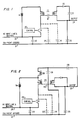
- FIG. 1 A schematic of a high frequency AC model of single ended switching type power supply useful for considering the more prominent RFI common mode current paths is disclosed in Fig. 1. Since common mode RFI is being evaluated, the input 20 is shown symbolically as a single conductor combining the rectified input and neutral leads.
- the primary switching loop is an AC current path including power switch 10, primary winding 16 of power transformer 15 and battery 14 which may be considered as a low resistance AC signal path.
- the secondary winding 17 is connected through rectifying diode 22, and filter capacitor 23 to the output common lead 24.
- a control circuit 30 periodically drives power switch 10 on and off.
- the major source of RF current is caused by the high frequency switching of power transistor 10 which is periodically driven by the control circuit 30.
- the currents generated by the large transient voltage changes due to this switching are coupled to the equipment ground 21 by currents flowing through the parasitic or stray capacitors 18 and 29, shown in dotted form in Fig. 1, and filter capacitors 26 and 25 which are also shown in Fig. 1.
- Parasitic or stray capacitor 18 represents the equivalent lumped stray capacitance between the primary winding 16 and secondary winding 17 of transformer 15.
- Parasitic capacitor 29 represents an equivalent lumped stray capacitance coupling the primary winding 16 to equipment ground 21, and as shown is paralleled with the parasitic capacitor 19 of the power switching transistor's head sink mounting capacitance coupling its collector to equipment ground.
- Capacitor 25 is a filter capacitor added so that common mode RFI does not flow out the input leads.
- Filter capacitor 25 is shown coupling the input line 20 to equipment ground 21.
- this capacitor When this capacitor is increased in value to shunt RF current from the input and equipment ground leads 20 and 21, it automatically conducts more leakage current to the equipment ground noise whose value often exceeds code standards. Reducing the capacitor value, however, places more RF currents in the circuit access leads creating RFI problems.
- FIG. 2 A particular arrangement for eliminating undesired RF current is shown schematically in Fig. 2 as it is applied to the conceptual schematic model shown in Fig. 1.
- This particular arrangement utilizes an auxiliary transformer winding 136 and associated added capacitors 138 and 139 to prevent the flow of RF currents out of equipment ground 121, and into the AC input line and neutral 120 that are due to generated harmonic voltages caused by high frequency switching of the power switching device 110 on the primary side of the circuit.
- Added transformer winding 136 is connected in series with primary winding 16 and with the designated winding polarities, as shown.
- Capacitor 139 is added to couple winding 136 to equipment ground 121.
- a second capacitor 138 is added to couple the junction of winding 136 and capacitor 139 to the output 124.
- the winding 136 operates as a voltage source generating a voltage substantially equal and opposite to the voltages generating the unwanted RF currents.
- the capacitor 139 combines with the parasitic or stray capacitance 119 to evenly divide the two opposing voltages and neutralize current flow. This neutralizing arrangement is effective within a frequency range in which the voltages of windings 116 and 136 are substantially in phase. The same cancellation arrangement may be extended to cancel any additional unwanted RF circuits.
- Capacitor 138 is added in series to the winding 136 to neutralize current that is coupled by the primary winding to secondary winding stray capacitance 118, and hence allows the output circuitry to float with respect to equipment ground with little RFI current flow to ground. This eliminates the need for large bypass capacitors in the output filter circuitry.
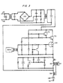
- a power train of an off-line switcher type power supply including circuitry to cancel unwanted RF currents to equipment ground is schematically shown in Fig. 3.
- An AC line signal applied to input leads 301 and 302 is rectified by fullwave rectifier 305 and coupled through a cascode connected pair of power switches.
- the first power switch includes a Darlington connected pair of transistors 310 and 311 connected in common base mode, and the second switch comprises a MOSFET 320 coupled in a common emitter mode and to the primary winding 316 of the power transformer 315.
- the Darlington connection is driven through a Baker clamp which is well known in the art and need not be disclosed in detail.
- the drive circuitry for MOSFET 320 is also conventional and believed to need no further description. This combination is adapted to achieve both switching speed and increased power handling capacity. Operation of this power supply is believed to be readily understood by those skilled in the art from the schematic of Fig. 3, and further description is believed unnecessary.
- Output is derived from the secondary winding 317.
- An auxiliary winding 336 is magnetically coupled to and connected in series with the primary winding 316.
- a capacitor 339 connects winding 336 to equipment ground 321. Winding 336 is oriented so as to generate a voltage of equal magnitude and opposite phase to a voltage across winding 316.
- the series capacitor 339 stores a voltage to oppose and neutralize a corresponding voltage across the stray capacitance from the primary winding 316 to equipment ground.
- This auxiliary circuitry operates in connection with the power supply to neutralize the RF currents and prevents their circulating to equipment ground, and additionally reduces the lower frequency leakage currents.
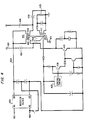
- Another switching type power supply includes added neutralizing circuit to neutralize RF currents that flow through a parasitic capacitor 419 from a primary winding and a power transistor mounting to equipment ground 421, and through parasitic capacitor 418 from primary winding 416 to secondary winding 417.
- Input power at terminals 401 and 402 is passed through rectifier filter 403 and line 404, through primary winding 416 and power switch 410.
- the power switch 410 is driven by control circuit 430 via drive transistor 420 to periodically couple primary winding 416 to the input power and enable transfer of power through power transformer 415 to the output load 425.
- the switching action of power switch 410 generates high frequency transients which are coupled to equipment ground 421 and to the secondary winding 417 by the stray capacitances 419 and 418, respectively.
- the currents due to these transients are nullified according to the invention by adding an auxiliary winding 436 to generate an equal but opposite voltage waveform to that generated in winding 416, and the addition of two voltage balancing capacitors 438 and 439 to neutralize the transient responsive ground currents on both primary and secondary sides of the circuit.
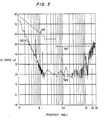
- the generated or emitted RFI of the circuit of Fig. 4 is compared to VDE standards in the graph of Fig. 5.
- the dotted line 501 shows the limits of RFI permitted by the VDE standard, and the amplitude of emitted RFI is shown by the curves 502 at various frequencies. It is apparent that the peak values of RFI over the frequency range of 10 KHz to 1 MHz is substantially below the permitted limit values of line 501. These values are low when compared with the normal expected values even where complicated RFI filtering circuits are utilized.
Landscapes
- Engineering & Computer Science (AREA)
- Power Engineering (AREA)
- Physics & Mathematics (AREA)
- Electromagnetism (AREA)
- Dc-Dc Converters (AREA)
- Power Conversion In General (AREA)
- Inverter Devices (AREA)
- Electronic Switches (AREA)
- Noise Elimination (AREA)
Claims (6)
Applications Claiming Priority (2)
| Application Number | Priority Date | Filing Date | Title |
|---|---|---|---|
| US06/789,392 US4625270A (en) | 1985-10-21 | 1985-10-21 | RFI suppression technique for switching circuits |
| US789392 | 1985-10-21 |
Publications (2)
| Publication Number | Publication Date |
|---|---|
| EP0243403A1 EP0243403A1 (de) | 1987-11-04 |
| EP0243403B1 true EP0243403B1 (de) | 1990-06-06 |
Family
ID=25147513
Family Applications (1)
| Application Number | Title | Priority Date | Filing Date |
|---|---|---|---|
| EP86906193A Expired EP0243403B1 (de) | 1985-10-21 | 1986-09-29 | Anordnung zur unterdrückung von hochfrequenzstörungen für schaltnetzteile |
Country Status (7)
| Country | Link |
|---|---|
| US (1) | US4625270A (de) |
| EP (1) | EP0243403B1 (de) |
| JP (1) | JPS63501679A (de) |
| CA (1) | CA1275440C (de) |
| DE (1) | DE3671816D1 (de) |
| ES (1) | ES2003395A6 (de) |
| WO (1) | WO1987002532A1 (de) |
Families Citing this family (17)
| Publication number | Priority date | Publication date | Assignee | Title |
|---|---|---|---|---|
| US4673851A (en) * | 1986-03-31 | 1987-06-16 | General Motors Corporation | PWM motor operating system with RFI suppression |
| DE4418886A1 (de) * | 1994-05-30 | 1995-12-07 | Patent Treuhand Ges Fuer Elektrische Gluehlampen Mbh | Getaktete Stromversorgung zum Betreiben elektrischer Lampen |
| DE4436464A1 (de) * | 1994-10-12 | 1996-04-18 | Patent Treuhand Ges Fuer Elektrische Gluehlampen Mbh | Getaktete Stromversorgung zum Betreiben von Glühlampen |
| DE19516641A1 (de) * | 1995-05-05 | 1996-11-07 | Siemens Ag | Entstörte Baugruppe |
| US5646498A (en) * | 1995-08-07 | 1997-07-08 | Eaton Corporation | Conducted emission radiation suppression in inverter drives |
| JP3331881B2 (ja) * | 1995-12-21 | 2002-10-07 | 三菱電機株式会社 | インバータ装置、圧縮機 |
| DE19702343A1 (de) * | 1997-01-23 | 1998-07-30 | Tridonic Bauelemente | Elektronischer Transformator |
| DE19817569A1 (de) * | 1998-04-20 | 1999-10-21 | Tridonic Bauelemente | Elektronischer Transformator |
| DE19903904A1 (de) * | 1999-02-01 | 2000-08-03 | Tridonic Bauelemente | Elektronischer Transformator zum Betreiben einer Last |
| US6094365A (en) * | 1999-10-20 | 2000-07-25 | Chiao; Po-Lun | Power supply device of switching mode with leakage current protection circuit |
| US6653691B2 (en) | 2000-11-16 | 2003-11-25 | Silicon Semiconductor Corporation | Radio frequency (RF) power devices having faraday shield layers therein |
| GB2447324B (en) * | 2008-02-21 | 2009-01-28 | Cambridge Semiconductor Ltd | Noise reduction systems and methods |
| JP5577296B2 (ja) * | 2010-06-09 | 2014-08-20 | 本田技研工業株式会社 | 半導体装置 |
| JP5995572B2 (ja) * | 2011-08-31 | 2016-09-21 | キヤノン株式会社 | ラインフィルタ、ラインフィルタを搭載したスイッチング電源及び画像形成装置 |
| EP4257066A3 (de) * | 2016-05-31 | 2023-11-29 | Stryker Corporation | Steuerpult mit transformator mit einer leckagesteuerungswicklung und einem kondensator |
| US10243453B1 (en) * | 2017-09-27 | 2019-03-26 | Apple Inc. | Common mode noise cancelation in power converters |
| EP3720372B1 (de) | 2017-12-06 | 2024-09-18 | Stryker Corporation | System zur steuerung des leckstroms eines patienten in einem chirurgischen system |
Family Cites Families (11)
| Publication number | Priority date | Publication date | Assignee | Title |
|---|---|---|---|---|
| US31638A (en) * | 1861-03-05 | Mode of preserving butter | ||
| US3339082A (en) * | 1965-02-26 | 1967-08-29 | Dielectric Products Engineerin | A.c. power supply system having alternate sources of supply |
| US4030024A (en) * | 1976-07-02 | 1977-06-14 | Raytheon Company | Switching power supply with floating internal supply circuit |
| US4212053A (en) * | 1978-07-31 | 1980-07-08 | Venus Scientific Inc. | D.C. to D.C. Converter utilizing resonant inductor to neutralize capacitive losses |
| JPS5660004A (en) * | 1979-10-19 | 1981-05-23 | Sony Corp | Parts of insulated inductance |
| USRE31638E (en) | 1980-06-13 | 1984-07-31 | Tcl, Inc. | Wideband transceiver with EMI suppression |
| US4377842A (en) * | 1980-10-06 | 1983-03-22 | International Business Machines Corporation | Flyback voltage control |
| US4439741A (en) * | 1982-06-28 | 1984-03-27 | Motorola, Inc. | Stabilized high efficiency radio frequency amplifier |
| US4449174A (en) * | 1982-11-30 | 1984-05-15 | Bell Telephone Laboratories, Incorporated | High frequency DC-to-DC converter |
| JPS59129571A (ja) * | 1983-01-14 | 1984-07-25 | Tdk Corp | スイツチング電源 |
| JPS61273173A (ja) * | 1985-05-29 | 1986-12-03 | Hitachi Ltd | スイツチング電源回路 |
-
1985
- 1985-10-21 US US06/789,392 patent/US4625270A/en not_active Expired - Lifetime
-
1986
- 1986-09-29 EP EP86906193A patent/EP0243403B1/de not_active Expired
- 1986-09-29 WO PCT/US1986/002057 patent/WO1987002532A1/en not_active Ceased
- 1986-09-29 JP JP61505488A patent/JPS63501679A/ja active Pending
- 1986-09-29 DE DE8686906193T patent/DE3671816D1/de not_active Expired - Fee Related
- 1986-10-20 CA CA000520832A patent/CA1275440C/en not_active Expired - Fee Related
- 1986-10-20 ES ES8602683A patent/ES2003395A6/es not_active Expired
Also Published As
| Publication number | Publication date |
|---|---|
| US4625270A (en) | 1986-11-25 |
| DE3671816D1 (de) | 1990-07-12 |
| ES2003395A6 (es) | 1988-11-01 |
| WO1987002532A1 (en) | 1987-04-23 |
| EP0243403A1 (de) | 1987-11-04 |
| JPS63501679A (ja) | 1988-06-23 |
| CA1275440C (en) | 1990-10-23 |
Similar Documents
| Publication | Publication Date | Title |
|---|---|---|
| EP0243403B1 (de) | Anordnung zur unterdrückung von hochfrequenzstörungen für schaltnetzteile | |
| JP4065008B2 (ja) | 分散型dc電源ネットワーク | |
| US5646498A (en) | Conducted emission radiation suppression in inverter drives | |
| US5262932A (en) | Power converter | |
| US5255174A (en) | Regulated bi-directional DC-to-DC voltage converter which maintains a continuous input current during step-up conversion | |
| US4888675A (en) | Switching power supply filter | |
| EP1289108B1 (de) | Vorrichtung zur Reduzierung von Stromrauschen in Leistungskonvertern | |
| KR100544758B1 (ko) | 교류 라인에 연결된 능동 공통 모드 필터 | |
| US4654771A (en) | Switched power supply comprising a free-running flow converter and electrically separated control loop | |
| US4686614A (en) | Reduced EMI noise in switched-mode power supply | |
| JPH06261451A (ja) | 分配電力システム | |
| WO1985002067A1 (en) | Switch current sensing with snubber current suppression in a push-pull converter | |
| US5390099A (en) | Line-powered, phase-control circuit | |
| US6867575B2 (en) | Switching mode power supply incorporating power line filter | |
| EP1658669A4 (de) | Vorrichtung zur rauschstromverminderung in stromwandlern | |
| Nagrial et al. | EMI/EMC issues in switch mode power supplies (SMPS) | |
| WO1991010280A1 (en) | A power inverter snubber circuit | |
| US4680687A (en) | Switch-mode power supply having a free-running forward converter | |
| JP3473853B2 (ja) | スイッチング電源装置 | |
| US20040141275A1 (en) | Active EMI filter for power switching circuit output | |
| US4660133A (en) | Switched power pack with free-wheeling flow converter and switched controller at a secondary side | |
| CA2052345A1 (en) | Power supply circuit | |
| Ninomiya et al. | EMI issues in switching power converters | |
| RU2637491C1 (ru) | Источник электропитания приемопередающего модуля | |
| JPH0697842B2 (ja) | スイッチングレギュレータ |
Legal Events
| Date | Code | Title | Description |
|---|---|---|---|
| PUAI | Public reference made under article 153(3) epc to a published international application that has entered the european phase |
Free format text: ORIGINAL CODE: 0009012 |
|
| AK | Designated contracting states |
Kind code of ref document: A1 Designated state(s): DE GB IT NL SE |
|
| 17P | Request for examination filed |
Effective date: 19870924 |
|
| 17Q | First examination report despatched |
Effective date: 19890926 |
|
| GRAA | (expected) grant |
Free format text: ORIGINAL CODE: 0009210 |
|
| AK | Designated contracting states |
Kind code of ref document: B1 Designated state(s): DE GB IT NL SE |
|
| REF | Corresponds to: |
Ref document number: 3671816 Country of ref document: DE Date of ref document: 19900712 |
|
| ITF | It: translation for a ep patent filed | ||
| PLBE | No opposition filed within time limit |
Free format text: ORIGINAL CODE: 0009261 |
|
| STAA | Information on the status of an ep patent application or granted ep patent |
Free format text: STATUS: NO OPPOSITION FILED WITHIN TIME LIMIT |
|
| 26N | No opposition filed | ||
| ITTA | It: last paid annual fee | ||
| EAL | Se: european patent in force in sweden |
Ref document number: 86906193.7 |
|
| PGFP | Annual fee paid to national office [announced via postgrant information from national office to epo] |
Ref country code: NL Payment date: 20010618 Year of fee payment: 16 |
|
| PGFP | Annual fee paid to national office [announced via postgrant information from national office to epo] |
Ref country code: SE Payment date: 20010831 Year of fee payment: 16 |
|
| REG | Reference to a national code |
Ref country code: GB Ref legal event code: IF02 |
|
| PGFP | Annual fee paid to national office [announced via postgrant information from national office to epo] |
Ref country code: GB Payment date: 20020808 Year of fee payment: 17 |
|
| PG25 | Lapsed in a contracting state [announced via postgrant information from national office to epo] |
Ref country code: SE Free format text: LAPSE BECAUSE OF NON-PAYMENT OF DUE FEES Effective date: 20020930 |
|
| PGFP | Annual fee paid to national office [announced via postgrant information from national office to epo] |
Ref country code: DE Payment date: 20020930 Year of fee payment: 17 |
|
| PG25 | Lapsed in a contracting state [announced via postgrant information from national office to epo] |
Ref country code: NL Free format text: LAPSE BECAUSE OF NON-PAYMENT OF DUE FEES Effective date: 20030401 |
|
| EUG | Se: european patent has lapsed | ||
| PG25 | Lapsed in a contracting state [announced via postgrant information from national office to epo] |
Ref country code: GB Free format text: LAPSE BECAUSE OF NON-PAYMENT OF DUE FEES Effective date: 20030929 |
|
| PG25 | Lapsed in a contracting state [announced via postgrant information from national office to epo] |
Ref country code: DE Free format text: LAPSE BECAUSE OF NON-PAYMENT OF DUE FEES Effective date: 20040401 |
|
| GBPC | Gb: european patent ceased through non-payment of renewal fee |
Effective date: 20030929 |
|
| PG25 | Lapsed in a contracting state [announced via postgrant information from national office to epo] |
Ref country code: IT Free format text: LAPSE BECAUSE OF NON-PAYMENT OF DUE FEES Effective date: 20050929 |