EP0242682B1 - Dispositif pour la fixation de composants électriques sur une plaque-support - Google Patents
Dispositif pour la fixation de composants électriques sur une plaque-support Download PDFInfo
- Publication number
- EP0242682B1 EP0242682B1 EP87105041A EP87105041A EP0242682B1 EP 0242682 B1 EP0242682 B1 EP 0242682B1 EP 87105041 A EP87105041 A EP 87105041A EP 87105041 A EP87105041 A EP 87105041A EP 0242682 B1 EP0242682 B1 EP 0242682B1
- Authority
- EP
- European Patent Office
- Prior art keywords
- engaging
- leg
- supporting board
- mounting arrangement
- arrangement according
- Prior art date
- Legal status (The legal status is an assumption and is not a legal conclusion. Google has not performed a legal analysis and makes no representation as to the accuracy of the status listed.)
- Expired - Lifetime
Links
Images
Classifications
-
- H—ELECTRICITY
- H05—ELECTRIC TECHNIQUES NOT OTHERWISE PROVIDED FOR
- H05K—PRINTED CIRCUITS; CASINGS OR CONSTRUCTIONAL DETAILS OF ELECTRIC APPARATUS; MANUFACTURE OF ASSEMBLAGES OF ELECTRICAL COMPONENTS
- H05K3/00—Apparatus or processes for manufacturing printed circuits
- H05K3/30—Assembling printed circuits with electric components, e.g. with resistor
- H05K3/306—Lead-in-hole components, e.g. affixing or retention before soldering, spacing means
-
- H—ELECTRICITY
- H05—ELECTRIC TECHNIQUES NOT OTHERWISE PROVIDED FOR
- H05K—PRINTED CIRCUITS; CASINGS OR CONSTRUCTIONAL DETAILS OF ELECTRIC APPARATUS; MANUFACTURE OF ASSEMBLAGES OF ELECTRICAL COMPONENTS
- H05K7/00—Constructional details common to different types of electric apparatus
- H05K7/02—Arrangements of circuit components or wiring on supporting structure
- H05K7/12—Resilient or clamping means for holding component to structure
-
- H—ELECTRICITY
- H05—ELECTRIC TECHNIQUES NOT OTHERWISE PROVIDED FOR
- H05K—PRINTED CIRCUITS; CASINGS OR CONSTRUCTIONAL DETAILS OF ELECTRIC APPARATUS; MANUFACTURE OF ASSEMBLAGES OF ELECTRICAL COMPONENTS
- H05K2201/00—Indexing scheme relating to printed circuits covered by H05K1/00
- H05K2201/10—Details of components or other objects attached to or integrated in a printed circuit board
- H05K2201/10007—Types of components
- H05K2201/1003—Non-printed inductor
-
- H—ELECTRICITY
- H05—ELECTRIC TECHNIQUES NOT OTHERWISE PROVIDED FOR
- H05K—PRINTED CIRCUITS; CASINGS OR CONSTRUCTIONAL DETAILS OF ELECTRIC APPARATUS; MANUFACTURE OF ASSEMBLAGES OF ELECTRICAL COMPONENTS
- H05K2201/00—Indexing scheme relating to printed circuits covered by H05K1/00
- H05K2201/10—Details of components or other objects attached to or integrated in a printed circuit board
- H05K2201/10431—Details of mounted components
- H05K2201/10568—Integral adaptations of a component or an auxiliary PCB for mounting, e.g. integral spacer element
-
- H—ELECTRICITY
- H05—ELECTRIC TECHNIQUES NOT OTHERWISE PROVIDED FOR
- H05K—PRINTED CIRCUITS; CASINGS OR CONSTRUCTIONAL DETAILS OF ELECTRIC APPARATUS; MANUFACTURE OF ASSEMBLAGES OF ELECTRICAL COMPONENTS
- H05K2201/00—Indexing scheme relating to printed circuits covered by H05K1/00
- H05K2201/10—Details of components or other objects attached to or integrated in a printed circuit board
- H05K2201/10431—Details of mounted components
- H05K2201/10598—Means for fastening a component, a casing or a heat sink whereby a pressure is exerted on the component towards the PCB
Definitions
- the invention relates to a fastening arrangement according to the preamble of claim 1.
- the procedure for connecting a sheet metal part to another component is such that a hook-like projection protruding from the sheet metal part is formed by a plastically deformable one
- the web is connected to the sheet metal part and is permanently deformed by inserting, for example, a screwdriver into a slot in the sheet metal part is that the hook on the approach engages behind the circuit board.
- a fixed stop protruding from the sheet metal part in the recess of the printed circuit board prevents displacement of the sheet metal part relative to the printed circuit board.
- the sheet metal part itself can be supported with additional surfaces from above on the circuit board.
- Another fastening means for the arrangement of components which can be, for example, a light indicator and switching means (DE-A-2 714 168), on a printed circuit board is that opposing, mutually facing hook projections are provided with locking legs which have a common slot, for example one Reach behind the printed circuit board, furthermore supporting webs are arranged on the component, which extend down to the surface of the printed circuit board.
- components which can be, for example, a light indicator and switching means (DE-A-2 714 168)
- opposing, mutually facing hook projections are provided with locking legs which have a common slot, for example one Reach behind the printed circuit board, furthermore supporting webs are arranged on the component, which extend down to the surface of the printed circuit board.
- radio interference suppression choke On a printed circuit board; it is understood, however, that the invention is not limited in its application to a radio interference suppression choke, but can generally serve to fasten any electronic and electrical components and components on a carrier plate, in particular large and heavy components such as transformers, capacitors, relays, plugs and the like . the like
- radio interference suppression chokes or current attenuation chokes possibly both chokes combined together with different cores, namely a ferrite core and an iron powder core, had to be attached to carrier plates in such a way that the respective cores were first coated with an insulating plastic layer or another layer, for example by a dipping process , and then a ring shape was placed on it having cores usually applied by automatic winding machines the electrical windings.
- the further fastening and processing steps then consisted in that a throttle constructed in this way was inserted into a plastic cup and then poured, whereupon the cup is then fastened in a suitable manner, usually with the aid of screws, to the carrier plate.
- the invention is therefore based on the object of improving a fastening arrangement of the type mentioned at the outset in such a way that, on the one hand, any components can be quickly and easily attached to an associated carrier plate, in particular a printed circuit board, preferably at the same time also providing means for producing the electrical connections, and which, on the other hand, ensures that perfect and safe storage on the printed circuit board is ensured even with considerable loads.
- the invention secures the simultaneous fastening and positioning of the electrical supply lines, the actual electrical component being securely accommodated in the associated holder.
- each latching leg is securely clamped and fixed in its receiving opening, that is to say in the carrier plate opening which receives it.
- a carrier plate opening in the case of the usual, known per se locking leg fixation, in which there is an extension projecting a locking lug perpendicular to the direction of insertion, must have at least one opening cross section which is as large as the head of the respective locking leg carrying the laterally projecting locking lug, so that after reaching behind the backing plate back surface there is necessarily always a spacing gap which is as large as the projection formed by the latching nose in the transverse direction, because otherwise the respective latching leg could not be passed through the corresponding receiving opening.
- a fixing leg is arranged adjacent to each latching leg so that when the latching leg engages behind the carrier plate after elastic retraction with the latching nose, latching leg on the one hand and fixing leg on the other hand in the cutout of the carrier plate or printed circuit board on both sides, optionally under one certain pre-tension, so that each individual fastening point is secured and held immovably.
- the fixation leg provides its own height stop, which is arranged in the corresponding distance relationship to the lower edge of the locking tab projecting in the transverse direction, for play-free height fixing, in a further embodiment it is also possible to compensate for the thickness tolerance of the support plate by the height stop being resilient in the tolerance field is trained.
- an additional securing of the preferably external locking legs to one another against backing away can be carried out by clipping an additional locking plate into a receiving opening of the printed circuit board carrying the component from the rear, in such a way that the fixing disk is in direct contact with the locking leg rear surfaces for securing whose immovable fixation results.
- a choke for example motor choke for radio interference suppression and / or current damping in electrical devices on a suitable printed circuit board or printed circuit board
- the choke as a toroidal core choke with two Ring cores made of different materials (ferrite core, iron powder core) and both cores surrounded by a corresponding electrical winding.
- the invention relates to any electrical component or can be applied to such an electrical component if it is to be fastened to a carrier board, which in particular can be a printed circuit board or printed circuit board.
- the housing can, as is understood , at other components may also be merely a lower surface supporting or supporting this component, from which the actual fastening and locking means relating to the subject matter of the present invention, which are generally designated by 12 in FIG. 2, emanate. Therefore, other components, such as relays, larger capacitor cups and.
- the intermediate part, which stores the actual electrical component can also be a half-cup, an injection-molded lower surface or the like, preferably made of plastic, from which the fastening and locking means 12 then extend in the direction of the printed circuit board which supports the whole.
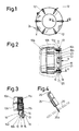
- these latching means consist of a first latch leg 13, known per se, formed from an extension or web 14 projecting downward from the housing 10a, 10b and a crosspiece attached to the latter Latch 15.
- the electrical component to be explained here is a toroidal core choke
- six such locking means 12 are provided, evenly distributed over the circumference, in the exemplary embodiment shown;
- any number of such locking means 12 can be provided, for example one in each corner in the case of a quadrangular shape, three in the case of round shapes and possibly only two in the case of narrower components to be fastened opposite each other Locking means.
- fixing leg 16 adjacent to at least one, preferably to each locking leg 13, a so-called fixing element, which is referred to below as fixing leg 16, is arranged and positioned at a distance from the locking leg 13 such that there is no size or design between the two critical slot 17 results, which in any case ensures that the detent leg 13 can perform its task, which is also known per se, namely by retreating in the direction of the arrow A (see FIG. 2), this movement being caused by the sliding of the front detent bevel surface 18 is effected in the respectively assigned opening of the printed circuit board or printed circuit board 20 to ensure that it is clipped in and the resulting fastening of the component to the printed circuit board.
- the locking leg 13 therefore moves briefly in the direction of the fixed fixing leg 16, which is rigid in the context of the circumstances considered here, and after passing through the opening in the printed circuit board 20 again takes up the original distance, the lower locking surface of the locking lug then engages behind the circuit board 20.
- the fixing leg 16 in its assignment to the latching leg 13 simultaneously takes on two further tasks for this fastening and locking, namely firstly due to a stop surface 16a the height fixing of the component, because as can be seen from the illustration in FIG. 2, corresponds practically to the distance of the stop surface 16a to the lower locking surface 19 of the locking lug 17 the PCB thickness with only enough tolerance that the locking leg can safely get into its starting position after locking. It is also possible here to compensate for the thickness tolerance of the carrier plate by making the height stop resilient in the tolerance field.
- the fixing leg 16 also has a further stop surface 16b (see also FIG. 2), which, opposite the outer main stop surface 13a of the latching leg 13, ensures that the rectangular receiving cutout for the locking means 12 as a whole in the printed circuit board 20 after being clipped in is completely filled, and preferably still under a residual residual prestress between the locking leg 13 and the fixing leg 16, which can be achieved by appropriate distance measurements. This ensures that each locking means 12 completely fills the opening or receiving hole assigned to it in the printed circuit board after insertion and that there is no free space left which would allow the locking leg 13 to withstand strong forces from any direction, in particular from transverse directions in the opening in the print plate receiving it so that it may become detached from it.
- the printed circuit board 20 with its perforations can completely accommodate the locking means up to the height stop 16a formed by the fixing leg 16, and only in this end position can the latching lugs push outwards again and the back of the printed circuit board reach behind, the parts of the fixing leg 16 entering into the circuit board opening have a bevel 21, so that complete insertion and clipping is possible under all circumstances.
- an additional locking plate 22 can be provided, which has an outer circumference has, which corresponds to the free distance between the inner locking leg surfaces when they are in their fully engaged position, so that the locking plate 22 can then be used in the direction of arrow B from the back of the circuit board and held in a suitable manner.
- the locking plate 22 in any manner, e.g. can be designed as a locking washer and must also have a structure over its circumference only at the points at which it effectively rests on the rear surfaces of the locking legs 13.
- a further advantageous embodiment of the present invention consists in that at the same time, as shown at 24 in FIG. 1, on the outside laterally on the circumference of the carrier body for the component, in the illustrated embodiment of a toroidal core choke on the lower half-shell 11b, bushings 25 formed by projections are formed are, through the inner channel of an electrical connection line 26 (see. Fig. 4), optionally passed through bending and is held securely in its relative position up to the passage opening through the circuit board 20.
- These bushings 25 preferably protrude from the main bearing body for the component to the surface of the printed circuit board, so that when the entire component is clipped in, the wire end pieces 26a of the connecting leads then stripped in this case also pass through the associated holes in the printed circuit board.
Claims (12)
- Système de fixation d'éléments ou composants électriques ou électroniques sur une plaque support, en particulier une platine conductrice ou à circuit imprimé, dans lequel l'élément à fixer est équipé d'appendices (14) portant les dents d'accrochage (15) venant en prise sur la face arrière de la plaque support, tandis qu'au voisinage mais à une certaine distance de chaque appendice (14) constituant une patte d'arrêt (13), est disposée une patte de fixation (16) reposant au moins sur une autre partie de l'ouverture de la plaque support recevant la patte d'arrêt (13) et la patte de fixation (16), caractérisé en ce que la patte d'arrêt (13) lorsqu'on engage, pour le serrer, l'élément à fixer dans l'ouverture de la plaque support, commence par reculer élastiquement pour pouvoir ensuite venir en prise par sa dent d'accrochage (15) sur la face arrière de la plaque support, tandis que pour assurer simultanément une fixation latérale au moyen de la patte de fixation (16), il est prévu sur cette patte une surface de butée de profil (16a) déterminant la hauteur à obtenir, la distance entre cette surface (16a) et la surface d'accrochage (19) de la dent (15) étant sensiblement égale à l'épaisseur de la plaque support.
- Système de fixation selon la revendication 1, caractérisé en ce que la surface de butée (16a) portée par la patte de fixation (16) et reposant sur l'autre partie de l'ouverture de la plaque support fait face à la partie de l'ouverture sur laquelle est en prise la dent d'accrochage (15) de la patte d'arrêt (13).
- Système de fixation selon la revendication 1 ou 2, caractérisé en ce que la distance séparant sous la forme d'une encoche (17) la face de patte d'arrêt et la patte de fixation est dimensionnée de manière que, lors du serrage, dans l'ouverture de la plaque support, la patte d'arrêt (13) puisse reculer suffisamment pour que la face d'accrochage de la dent puisse passer à travers l'ouverture de la plaque et venir en prise derrière celle-ci, la distance entre la surface antérieure de la patte d'arrêt (13) en appui dans l'ouverture de la plaque et la surface de butée (16b), orientée vers l'arrière de la patte de fixation (16) étant dimensionnée de manière à ce que ces surfaces se trouvent obligatoirement, de préférence sous l'effet de rappel résultant de l'élasticité de la patte d'arrêt (13), logées avec serrage dans l'ouverture de la plaque support.
- Système de fixation selon l'une des revendications 1 à 3, caractérisé en ce que la saillie (16c) de la patte de fixation (16) qui porte la surface de butée arrière (16b) de la patte (16) et qui traverse au moins partiellement l'ouverture de la plaque support, présente une partie oblique (21) facilitant l'introduction dans l'ouverture rectangulaire correspondante de la plaque support, de chacun des ensembles de verrouillage (12) constitués par une patte d'arrêt (13) et une patte de fixation (16).
- Système de fixation selon une des revendications 1 à 4, caractérisé en ce que chaque ensemble de verrouillage (12) est réalisé solidaire du fond de la pièce ou de l'élément à fixer, par injection monobloc, un certain nombre de moyens d'arrêt étant répartis à la périphérie de l'élément.
- Système de fixation selon une des revendications 1 à 5, caractérisé en ce qu'il est prévu une partie de boîtier, par exemple une demicuvette (10b), servant de logement à l'élément à fixer et aux divers ensembles de verrouillage (12) et munie de passages (25) en forme d'appendices (24) pour recevoir les raccords électriques (26).
- Système de fixation selon la revendication 6, caractérisé en ce que les appendices (24) servant de passage aux raccords électriques (26) s'étendent jusqu'à la limite de la face supérieure de la plaque conductrice, assurant ainsi un prépositionnement précis pour la réalisation des liaisons électriques.
- Système de fixation selon une des revendications 1 à 7, caractérisé en ce qu'une butée supplémentaire est prévue sous la forme d'une platine de verrouillage (22) qui vient, elle-même s'appuyer en butée sur les faces arrière, opposées aux dents d'accrochage, des pattes d'arrêt (13), en poussant celles-ci en position irréversible contre les parois antérieures correspondantes de la découpe constituant l'ouverture du panneau support.
- Système de fixation selon la revendication 8, caractérisé en ce que l'élément de butée fixant les pattes d'arrêt (13) est constitué d'un disque d'arrêt (22) de diamètre extérieur correspondant au diamètre intérieur des pattes d'arrêt (13) en position bloquée, ainsi que d'organes de maintien portés par la plaque conductrice (20) correspondante.
- Système de fixation selon la revendication 8 ou 9, caractérisé en ce que la plaque de verrouillage (22) est équipée d'un nez (22a) passant à travers une ouverture centrale de la plaque conductrice (20) et qui, au moyen de dents d'accrochage (24) en prise avec la face, côté élément à fixer, de la plaque conductrice (20) se trouve verrouillée sur cette plaque.
- Système de fixation selon une des revendications 1 à 10, caractérisé en ce que la patte de fixation rigide, par rapport à la patte d'arrêt élastique, présente selon la direction du chanfrein de la patte d'arrêt, une dimension supérieure de sorte que les pattes de fixation se trouvent disposées en étoile par rapport au centre de l'élément à fixer.
- Système de fixation selon une des revendications 1 à 11, caractérisé en ce que, pour compenser les tolérances d'épaisseur de la plaque support, la butée de profil (16a) présente une élasticité couvrant la plage de tolérance.
Priority Applications (1)
| Application Number | Priority Date | Filing Date | Title |
|---|---|---|---|
| AT87105041T ATE86822T1 (de) | 1986-04-24 | 1987-04-04 | Befestigungseinrichtung fuer elektrische bauelemente auf einer traegerplatte. |
Applications Claiming Priority (2)
| Application Number | Priority Date | Filing Date | Title |
|---|---|---|---|
| DE3613863 | 1986-04-24 | ||
| DE19863613863 DE3613863A1 (de) | 1986-04-24 | 1986-04-24 | Befestigungseinrichtung fuer elektrische bauelemente auf einer traegerplatte |
Publications (3)
| Publication Number | Publication Date |
|---|---|
| EP0242682A2 EP0242682A2 (fr) | 1987-10-28 |
| EP0242682A3 EP0242682A3 (en) | 1989-10-18 |
| EP0242682B1 true EP0242682B1 (fr) | 1993-03-10 |
Family
ID=6299430
Family Applications (1)
| Application Number | Title | Priority Date | Filing Date |
|---|---|---|---|
| EP87105041A Expired - Lifetime EP0242682B1 (fr) | 1986-04-24 | 1987-04-04 | Dispositif pour la fixation de composants électriques sur une plaque-support |
Country Status (3)
| Country | Link |
|---|---|
| EP (1) | EP0242682B1 (fr) |
| AT (1) | ATE86822T1 (fr) |
| DE (2) | DE3613863A1 (fr) |
Families Citing this family (5)
| Publication number | Priority date | Publication date | Assignee | Title |
|---|---|---|---|---|
| DE4213578C2 (de) * | 1992-04-24 | 1994-04-28 | Bsg Schalttechnik | Torsionsschnappverbindung zur Befestigung von Bauelementen auf Leiterplatten |
| DE4343325A1 (de) * | 1993-12-18 | 1995-06-22 | Telefunken Microelectron | Ventilsteuervorrichtung |
| DE4416146C2 (de) * | 1994-05-06 | 1999-06-10 | Amphenol Tuchel Elect | Rastbefestigungsmittel zur Befestigung eines Bauteils |
| DE10361452A1 (de) | 2003-12-23 | 2005-10-06 | Demag Cranes & Components Gmbh | Anordnung zum Befestigen von elektrischen und/oder elektronischen Bauteilen, insbesondere Leistungsbauteilen, an einer Platine und Gehäuse hiermit |
| DE102014224933A1 (de) | 2014-12-04 | 2016-06-09 | Würth Elektronik eiSos Gmbh & Co. KG | Bauelement-Steckverbindungsanordnung zum steckbaren Verbinden eines Bauelements mit einer Leiterplatte und Verfahren zur Herstellung einer derartigen Bauelement-Steckverbindungsanordnung |
Family Cites Families (2)
| Publication number | Priority date | Publication date | Assignee | Title |
|---|---|---|---|---|
| DE2714168A1 (de) * | 1977-03-30 | 1978-10-05 | Siemens Ag | Befestigungsmittel um bauelemente, insbesondere leuchtanzeige- und schaltmittel auf einer leiterplatte anzubringen |
| DE3006673A1 (de) * | 1980-02-22 | 1981-08-27 | Licentia Patent-Verwaltungs-Gmbh, 6000 Frankfurt | Verbindung eines blechteiles mit einem anderen bauteil |
-
1986
- 1986-04-24 DE DE19863613863 patent/DE3613863A1/de not_active Withdrawn
-
1987
- 1987-04-04 DE DE8787105041T patent/DE3784543D1/de not_active Expired - Fee Related
- 1987-04-04 EP EP87105041A patent/EP0242682B1/fr not_active Expired - Lifetime
- 1987-04-04 AT AT87105041T patent/ATE86822T1/de not_active IP Right Cessation
Also Published As
| Publication number | Publication date |
|---|---|
| DE3784543D1 (de) | 1993-04-15 |
| EP0242682A2 (fr) | 1987-10-28 |
| EP0242682A3 (en) | 1989-10-18 |
| ATE86822T1 (de) | 1993-03-15 |
| DE3613863A1 (de) | 1987-10-29 |
Similar Documents
| Publication | Publication Date | Title |
|---|---|---|
| DE3636065C1 (de) | Halterung von elektrischen Bauelementen auf einer Schaltungsplatte | |
| DE102004031707B4 (de) | Intelligenter Anschlusskasten für Kraftfahrzeuge | |
| DE3600361C2 (de) | Substrathalter in Integralbauweise | |
| EP0384014B1 (fr) | Dispositif pour positionner un support de bobine dans un boîtier en forme de pot | |
| DE102007038787A1 (de) | Leuchtmodul für eine Halbleiterlichtquellen-Leuchte und Halbleiterlichtquellen-Leuchte | |
| DE4428883C1 (de) | Einrichtung für Kraftfahrzeuge | |
| EP0982978B1 (fr) | Boítier, en particulier boítier de serrure avec interconnections électriques | |
| DE2511385C3 (de) | Elektrische Anschlußklemme | |
| EP0242682B1 (fr) | Dispositif pour la fixation de composants électriques sur une plaque-support | |
| DE102012202213A1 (de) | Befestigungsaufbau | |
| DE8221515U1 (de) | Sicherungshalter zur Aufnahme von Lamellensicherungen, insbesondere für Kraftfahrzeuge | |
| DE2044096A1 (de) | Möbel mit mindestens einer Anschlagtür | |
| DE3418894A1 (de) | Vorrichtung zur befestigung eines gegenstandes aus kunststoff, insbesondere eines halteelements, an einer traegerplatte | |
| EP1548907B1 (fr) | Dispositif de fixation de composants électroniques/électriques sur une platine et boîtier avec ce dispositif | |
| DE2839555A1 (de) | Antriebsanordnung in einem elektrischen geraet | |
| DE2942380A1 (de) | Fassung fuer eine sockellose lampe | |
| WO1997043552A1 (fr) | Dispositif permettant de fixer un appareil | |
| DE19839118C2 (de) | Konstruktionsanordnung für die Befestigung eines Bauelements auf einer gedruckten Leiterplatte und elektronische Geräte mit dieser Konstruktion | |
| WO2004023606A1 (fr) | Borne de traversee | |
| DD248682A1 (de) | Anordnung zur herstellung von elektrischen verbindungen in einem elektromotor | |
| WO2001052363A1 (fr) | Piece de connexion electrique | |
| DE4429984C1 (de) | Elektrisches oder elektronisches Gerät für ein Kraftfahrzeug | |
| DE4313739A1 (de) | Vorrichtung zum Befestigen eines zweiten Bauteils an einem ersten Bauteil | |
| DE3613862A1 (de) | Drossel oder uebertrager mit befestigungsmitteln auf einer leiterplatte | |
| DE102019215533B3 (de) | Fahrzeug, umfassend eine Antennenvorrichtung, sowie Antennenvorrichtung und Befestigungseinrichtung |
Legal Events
| Date | Code | Title | Description |
|---|---|---|---|
| PUAI | Public reference made under article 153(3) epc to a published international application that has entered the european phase |
Free format text: ORIGINAL CODE: 0009012 |
|
| AK | Designated contracting states |
Kind code of ref document: A2 Designated state(s): AT BE CH DE ES FR GB GR IT LI LU NL SE |
|
| PUAL | Search report despatched |
Free format text: ORIGINAL CODE: 0009013 |
|
| AK | Designated contracting states |
Kind code of ref document: A3 Designated state(s): AT BE CH DE ES FR GB GR IT LI LU NL SE |
|
| RHK1 | Main classification (correction) |
Ipc: H05K 7/12 |
|
| 17P | Request for examination filed |
Effective date: 19891121 |
|
| 17Q | First examination report despatched |
Effective date: 19910816 |
|
| GRAA | (expected) grant |
Free format text: ORIGINAL CODE: 0009210 |
|
| AK | Designated contracting states |
Kind code of ref document: B1 Designated state(s): AT BE CH DE ES FR GB GR IT LI LU NL SE |
|
| PG25 | Lapsed in a contracting state [announced via postgrant information from national office to epo] |
Ref country code: SE Effective date: 19930310 Ref country code: FR Effective date: 19930310 Ref country code: NL Effective date: 19930310 Ref country code: BE Effective date: 19930310 Ref country code: GR Free format text: LAPSE BECAUSE OF FAILURE TO SUBMIT A TRANSLATION OF THE DESCRIPTION OR TO PAY THE FEE WITHIN THE PRESCRIBED TIME-LIMIT Effective date: 19930310 Ref country code: GB Effective date: 19930310 Ref country code: IT Free format text: LAPSE BECAUSE OF FAILURE TO SUBMIT A TRANSLATION OF THE DESCRIPTION OR TO PAY THE FEE WITHIN THE PRE;WARNING: LAPSES OF ITALIAN PATENTS WITH EFFECTIVE DATE BEFORE 2007 MAY HAVE OCCURRED AT ANY TIME BEFORE 2007. THE CORRECT EFFECTIVE DATE MAY BE DIFFERENT FROM THE ONE RECORDED.SCRIBED TIME-LIMIT Effective date: 19930310 |
|
| REF | Corresponds to: |
Ref document number: 86822 Country of ref document: AT Date of ref document: 19930315 Kind code of ref document: T |
|
| PG25 | Lapsed in a contracting state [announced via postgrant information from national office to epo] |
Ref country code: AT Effective date: 19930404 |
|
| REF | Corresponds to: |
Ref document number: 3784543 Country of ref document: DE Date of ref document: 19930415 |
|
| PG25 | Lapsed in a contracting state [announced via postgrant information from national office to epo] |
Ref country code: CH Effective date: 19930430 Ref country code: LI Effective date: 19930430 Ref country code: LU Free format text: LAPSE BECAUSE OF NON-PAYMENT OF DUE FEES Effective date: 19930430 |
|
| PG25 | Lapsed in a contracting state [announced via postgrant information from national office to epo] |
Ref country code: ES Free format text: LAPSE BECAUSE OF FAILURE TO SUBMIT A TRANSLATION OF THE DESCRIPTION OR TO PAY THE FEE WITHIN THE PRESCRIBED TIME-LIMIT Effective date: 19930621 |
|
| EN | Fr: translation not filed | ||
| NLV1 | Nl: lapsed or annulled due to failure to fulfill the requirements of art. 29p and 29m of the patents act | ||
| GBV | Gb: ep patent (uk) treated as always having been void in accordance with gb section 77(7)/1977 [no translation filed] |
Effective date: 19930310 |
|
| REG | Reference to a national code |
Ref country code: CH Ref legal event code: PL |
|
| PG25 | Lapsed in a contracting state [announced via postgrant information from national office to epo] |
Ref country code: DE Effective date: 19940101 |
|
| PLBE | No opposition filed within time limit |
Free format text: ORIGINAL CODE: 0009261 |
|
| STAA | Information on the status of an ep patent application or granted ep patent |
Free format text: STATUS: NO OPPOSITION FILED WITHIN TIME LIMIT |
|
| 26N | No opposition filed |