EP0241274A2 - Lichtempfindliches Element - Google Patents
Lichtempfindliches Element Download PDFInfo
- Publication number
- EP0241274A2 EP0241274A2 EP87303041A EP87303041A EP0241274A2 EP 0241274 A2 EP0241274 A2 EP 0241274A2 EP 87303041 A EP87303041 A EP 87303041A EP 87303041 A EP87303041 A EP 87303041A EP 0241274 A2 EP0241274 A2 EP 0241274A2
- Authority
- EP
- European Patent Office
- Prior art keywords
- layer
- atoms
- light receiving
- receiving member
- substrate
- Prior art date
- Legal status (The legal status is an assumption and is not a legal conclusion. Google has not performed a legal analysis and makes no representation as to the accuracy of the status listed.)
- Granted
Links
- 239000000758 substrate Substances 0.000 claims abstract description 66
- XAGFODPZIPBFFR-UHFFFAOYSA-N aluminium Chemical compound [Al] XAGFODPZIPBFFR-UHFFFAOYSA-N 0.000 claims abstract description 59
- 229910052782 aluminium Inorganic materials 0.000 claims abstract description 58
- 239000000463 material Substances 0.000 claims abstract description 54
- 230000005764 inhibitory process Effects 0.000 claims description 41
- 238000002347 injection Methods 0.000 claims description 40
- 239000007924 injection Substances 0.000 claims description 40
- 238000010521 absorption reaction Methods 0.000 claims description 37
- 125000004429 atom Chemical group 0.000 claims description 32
- XUIMIQQOPSSXEZ-UHFFFAOYSA-N Silicon Chemical group [Si] XUIMIQQOPSSXEZ-UHFFFAOYSA-N 0.000 claims description 19
- 239000000470 constituent Substances 0.000 claims description 17
- 125000004435 hydrogen atom Chemical group [H]* 0.000 claims description 16
- 125000004432 carbon atom Chemical group C* 0.000 claims description 13
- 125000004433 nitrogen atom Chemical group N* 0.000 claims description 13
- 125000004430 oxygen atom Chemical group O* 0.000 claims description 13
- 125000005843 halogen group Chemical group 0.000 claims description 12
- 229910021478 group 5 element Inorganic materials 0.000 claims description 9
- ATJFFYVFTNAWJD-UHFFFAOYSA-N Tin Chemical group [Sn] ATJFFYVFTNAWJD-UHFFFAOYSA-N 0.000 claims description 7
- AZDRQVAHHNSJOQ-UHFFFAOYSA-N alumane Chemical group [AlH3] AZDRQVAHHNSJOQ-UHFFFAOYSA-N 0.000 claims description 6
- GNPVGFCGXDBREM-UHFFFAOYSA-N germanium atom Chemical group [Ge] GNPVGFCGXDBREM-UHFFFAOYSA-N 0.000 claims description 2
- 230000000737 periodic effect Effects 0.000 claims description 2
- 239000004411 aluminium Substances 0.000 claims 4
- 239000010410 layer Substances 0.000 description 242
- 239000007789 gas Substances 0.000 description 116
- 238000000151 deposition Methods 0.000 description 31
- 230000008021 deposition Effects 0.000 description 31
- 238000000034 method Methods 0.000 description 27
- BLRPTPMANUNPDV-UHFFFAOYSA-N Silane Chemical compound [SiH4] BLRPTPMANUNPDV-UHFFFAOYSA-N 0.000 description 19
- 239000002344 surface layer Substances 0.000 description 18
- 210000002381 plasma Anatomy 0.000 description 14
- 239000002994 raw material Substances 0.000 description 14
- 229910021420 polycrystalline silicon Inorganic materials 0.000 description 10
- 238000005229 chemical vapour deposition Methods 0.000 description 7
- 238000009792 diffusion process Methods 0.000 description 7
- 229910052799 carbon Inorganic materials 0.000 description 6
- 229910052757 nitrogen Inorganic materials 0.000 description 6
- 229910052710 silicon Inorganic materials 0.000 description 6
- VOITXYVAKOUIBA-UHFFFAOYSA-N triethylaluminium Chemical compound CC[Al](CC)CC VOITXYVAKOUIBA-UHFFFAOYSA-N 0.000 description 6
- 230000005587 bubbling Effects 0.000 description 5
- 239000010703 silicon Substances 0.000 description 5
- 206010034972 Photosensitivity reaction Diseases 0.000 description 4
- 238000007664 blowing Methods 0.000 description 4
- 230000007547 defect Effects 0.000 description 4
- QUZPNFFHZPRKJD-UHFFFAOYSA-N germane Chemical compound [GeH4] QUZPNFFHZPRKJD-UHFFFAOYSA-N 0.000 description 4
- 229910052986 germanium hydride Inorganic materials 0.000 description 4
- 230000001678 irradiating effect Effects 0.000 description 4
- 230000036211 photosensitivity Effects 0.000 description 4
- 229910045601 alloy Inorganic materials 0.000 description 3
- 239000000956 alloy Substances 0.000 description 3
- 238000011156 evaluation Methods 0.000 description 3
- 229910052751 metal Inorganic materials 0.000 description 3
- 239000002184 metal Substances 0.000 description 3
- 150000002739 metals Chemical class 0.000 description 3
- 238000005546 reactive sputtering Methods 0.000 description 3
- 230000001105 regulatory effect Effects 0.000 description 3
- 239000004065 semiconductor Substances 0.000 description 3
- WFKWXMTUELFFGS-UHFFFAOYSA-N tungsten Chemical compound [W] WFKWXMTUELFFGS-UHFFFAOYSA-N 0.000 description 3
- 229910052721 tungsten Inorganic materials 0.000 description 3
- 239000010937 tungsten Substances 0.000 description 3
- ZAMOUSCENKQFHK-UHFFFAOYSA-N Chlorine atom Chemical compound [Cl] ZAMOUSCENKQFHK-UHFFFAOYSA-N 0.000 description 2
- PXGOKWXKJXAPGV-UHFFFAOYSA-N Fluorine Chemical compound FF PXGOKWXKJXAPGV-UHFFFAOYSA-N 0.000 description 2
- 229910052787 antimony Inorganic materials 0.000 description 2
- 229910052796 boron Inorganic materials 0.000 description 2
- 229910052801 chlorine Inorganic materials 0.000 description 2
- 239000000460 chlorine Substances 0.000 description 2
- 229910052731 fluorine Inorganic materials 0.000 description 2
- 239000011737 fluorine Substances 0.000 description 2
- 229910052733 gallium Inorganic materials 0.000 description 2
- 238000005268 plasma chemical vapour deposition Methods 0.000 description 2
- 229910052697 platinum Inorganic materials 0.000 description 2
- ZCYVEMRRCGMTRW-UHFFFAOYSA-N 7553-56-2 Chemical compound [I] ZCYVEMRRCGMTRW-UHFFFAOYSA-N 0.000 description 1
- ZOXJGFHDIHLPTG-UHFFFAOYSA-N Boron Chemical compound [B] ZOXJGFHDIHLPTG-UHFFFAOYSA-N 0.000 description 1
- WKBOTKDWSSQWDR-UHFFFAOYSA-N Bromine atom Chemical compound [Br] WKBOTKDWSSQWDR-UHFFFAOYSA-N 0.000 description 1
- GYHNNYVSQQEPJS-UHFFFAOYSA-N Gallium Chemical compound [Ga] GYHNNYVSQQEPJS-UHFFFAOYSA-N 0.000 description 1
- NPPQSCRMBWNHMW-UHFFFAOYSA-N Meprobamate Chemical compound NC(=O)OCC(C)(CCC)COC(N)=O NPPQSCRMBWNHMW-UHFFFAOYSA-N 0.000 description 1
- OAICVXFJPJFONN-UHFFFAOYSA-N Phosphorus Chemical compound [P] OAICVXFJPJFONN-UHFFFAOYSA-N 0.000 description 1
- 241000791876 Selene Species 0.000 description 1
- WATWJIUSRGPENY-UHFFFAOYSA-N antimony atom Chemical compound [Sb] WATWJIUSRGPENY-UHFFFAOYSA-N 0.000 description 1
- 229910052785 arsenic Inorganic materials 0.000 description 1
- RQNWIZPPADIBDY-UHFFFAOYSA-N arsenic atom Chemical compound [As] RQNWIZPPADIBDY-UHFFFAOYSA-N 0.000 description 1
- 230000015572 biosynthetic process Effects 0.000 description 1
- 229910052797 bismuth Inorganic materials 0.000 description 1
- JCXGWMGPZLAOME-UHFFFAOYSA-N bismuth atom Chemical compound [Bi] JCXGWMGPZLAOME-UHFFFAOYSA-N 0.000 description 1
- GDTBXPJZTBHREO-UHFFFAOYSA-N bromine Substances BrBr GDTBXPJZTBHREO-UHFFFAOYSA-N 0.000 description 1
- 229910052794 bromium Inorganic materials 0.000 description 1
- 230000015556 catabolic process Effects 0.000 description 1
- 229910052804 chromium Inorganic materials 0.000 description 1
- 230000001276 controlling effect Effects 0.000 description 1
- 230000003247 decreasing effect Effects 0.000 description 1
- 230000006866 deterioration Effects 0.000 description 1
- 229910052732 germanium Inorganic materials 0.000 description 1
- 238000010438 heat treatment Methods 0.000 description 1
- 229910052738 indium Inorganic materials 0.000 description 1
- APFVFJFRJDLVQX-UHFFFAOYSA-N indium atom Chemical compound [In] APFVFJFRJDLVQX-UHFFFAOYSA-N 0.000 description 1
- 230000002401 inhibitory effect Effects 0.000 description 1
- 229910052740 iodine Inorganic materials 0.000 description 1
- 239000011630 iodine Substances 0.000 description 1
- 238000004519 manufacturing process Methods 0.000 description 1
- 239000007769 metal material Substances 0.000 description 1
- 239000000203 mixture Substances 0.000 description 1
- 229910052759 nickel Inorganic materials 0.000 description 1
- 229910052758 niobium Inorganic materials 0.000 description 1
- 229910052698 phosphorus Inorganic materials 0.000 description 1
- 229910000077 silane Inorganic materials 0.000 description 1
- 239000010935 stainless steel Substances 0.000 description 1
- 229910001220 stainless steel Inorganic materials 0.000 description 1
- 229910052715 tantalum Inorganic materials 0.000 description 1
- 229910052716 thallium Inorganic materials 0.000 description 1
- BKVIYDNLLOSFOA-UHFFFAOYSA-N thallium Chemical compound [Tl] BKVIYDNLLOSFOA-UHFFFAOYSA-N 0.000 description 1
- 229910052718 tin Inorganic materials 0.000 description 1
- 229910052719 titanium Inorganic materials 0.000 description 1
- 238000007738 vacuum evaporation Methods 0.000 description 1
- 229910052720 vanadium Inorganic materials 0.000 description 1
Images

Classifications
-
- G—PHYSICS
- G03—PHOTOGRAPHY; CINEMATOGRAPHY; ANALOGOUS TECHNIQUES USING WAVES OTHER THAN OPTICAL WAVES; ELECTROGRAPHY; HOLOGRAPHY
- G03G—ELECTROGRAPHY; ELECTROPHOTOGRAPHY; MAGNETOGRAPHY
- G03G5/00—Recording members for original recording by exposure, e.g. to light, to heat, to electrons; Manufacture thereof; Selection of materials therefor
- G03G5/02—Charge-receiving layers
- G03G5/04—Photoconductive layers; Charge-generation layers or charge-transporting layers; Additives therefor; Binders therefor
- G03G5/08—Photoconductive layers; Charge-generation layers or charge-transporting layers; Additives therefor; Binders therefor characterised by the photoconductive material being inorganic
- G03G5/082—Photoconductive layers; Charge-generation layers or charge-transporting layers; Additives therefor; Binders therefor characterised by the photoconductive material being inorganic and not being incorporated in a bonding material, e.g. vacuum deposited
- G03G5/08214—Silicon-based
- G03G5/08235—Silicon-based comprising three or four silicon-based layers
-
- G—PHYSICS
- G03—PHOTOGRAPHY; CINEMATOGRAPHY; ANALOGOUS TECHNIQUES USING WAVES OTHER THAN OPTICAL WAVES; ELECTROGRAPHY; HOLOGRAPHY
- G03G—ELECTROGRAPHY; ELECTROPHOTOGRAPHY; MAGNETOGRAPHY
- G03G5/00—Recording members for original recording by exposure, e.g. to light, to heat, to electrons; Manufacture thereof; Selection of materials therefor
- G03G5/02—Charge-receiving layers
- G03G5/04—Photoconductive layers; Charge-generation layers or charge-transporting layers; Additives therefor; Binders therefor
- G03G5/08—Photoconductive layers; Charge-generation layers or charge-transporting layers; Additives therefor; Binders therefor characterised by the photoconductive material being inorganic
- G03G5/082—Photoconductive layers; Charge-generation layers or charge-transporting layers; Additives therefor; Binders therefor characterised by the photoconductive material being inorganic and not being incorporated in a bonding material, e.g. vacuum deposited
- G03G5/08214—Silicon-based
- G03G5/0825—Silicon-based comprising five or six silicon-based layers
-
- G—PHYSICS
- G03—PHOTOGRAPHY; CINEMATOGRAPHY; ANALOGOUS TECHNIQUES USING WAVES OTHER THAN OPTICAL WAVES; ELECTROGRAPHY; HOLOGRAPHY
- G03G—ELECTROGRAPHY; ELECTROPHOTOGRAPHY; MAGNETOGRAPHY
- G03G5/00—Recording members for original recording by exposure, e.g. to light, to heat, to electrons; Manufacture thereof; Selection of materials therefor
- G03G5/02—Charge-receiving layers
- G03G5/04—Photoconductive layers; Charge-generation layers or charge-transporting layers; Additives therefor; Binders therefor
- G03G5/08—Photoconductive layers; Charge-generation layers or charge-transporting layers; Additives therefor; Binders therefor characterised by the photoconductive material being inorganic
- G03G5/082—Photoconductive layers; Charge-generation layers or charge-transporting layers; Additives therefor; Binders therefor characterised by the photoconductive material being inorganic and not being incorporated in a bonding material, e.g. vacuum deposited
- G03G5/08214—Silicon-based
- G03G5/08278—Depositing methods
Definitions
- This invention relates to the improvements in a conventional light receiving member having a photoconductive layer formed of a silicon containing amorphous material on a substrate constituted principally with aluminum material.
- a high resistance intermediate layer formed of a non-monocrystalline material containing silicon atoms as the main constituent atoms and at least one kind atoms selected from oxygen atoms, carbon atoms and nitrogen atoms or/and a charge injection inhibition layer formed of a non-monocrystalline material containing hydrogen atoms and/or halogen atoms in addition to silicon atoms, and a conductivity controlling element of Group III or Group V of the Periodic Table (hereinafter referred to as "Group III element” and “Group V element” respectively) respectively aiming at inhibiting electrons from being injected into the photoconductive layer from the side of the substrate at the time when the light receiving member is engaged in electrification process and permitting the photocarriers, which will be generated in the photoconductive layer and move toward the substrate side at the time when received irradiation of electromagnetic waves, to pass through the substrate side from the photoconductive layer.
- Group III element Group V of the Periodic Table
- IR absorption layer a layer functioning to absorb light in the long wavelength region
- IR absorption layer As such IR absorption layer, there has been proposed such that is formed of an amorphous material containing at least one kind atom selected from silicon atom (Si), germanium atom (Ge) and tin atom (Sn).
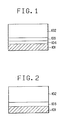
- Figure 2 is a schematic cross-sectional view illustrating the typical layer composition of the known light receiving member, in which are shown substrate 101, photoconductive layer 102 and high resistance intermediate layer, charge injection inhibition layer or IR absorption layer 103.
- the electroconductive substrate for. use in the known light receiving member having a photoconductive layer formed of an A-Si:H material or an A-Si(H,X) there have been used metals such as A&, Ni, Cr, Mo, Au, Nb, Ta, V, Ti, Pt, Pt, etc. or alloys of two or more of these metals such as stainless steel.
- metals such as A&, Ni, Cr, Mo, Au, Nb, Ta, V, Ti, Pt, Pt, etc. or alloys of two or more of these metals such as stainless steel.
- metallic materials the aluminum metal or alloys of which principal constituent is aluminum are most preferably used in the viewpoints of their lightness and treatment easiness and also in the economical viewpoint.
- these light receiving members are generally prepared by forming on a substrate each of the foregoing IR absorption layer, charge injection inhibition layer, high resistance intermediate layer and photoconductive layer by means of vacuum evaporation, thermal induced chemical vapor deposition, plasma chemical vapor deposition and reactive sputtering.
- aluminum substrate a substrate of which principal constituent is aluminum (hereinafter referred to as "aluminum substrate") using such film forming process, it is generally recognized that there are several problems as hereunder mentioned.
- the softening point of aluminum is in the range from 150°C to 200°C, when the aluminum substrate is heated to about 250°C and maintained at that temperature, a strain is apt to cause on the aluminum substrate during the film forming operation.
- This invention is aimed at eliminating the foregoing problems in the conventional light receiving member having a photoconductive layer formed of a silicon containing amorphous material in which an aluminum material being used as the substrate and providing an improved light receiving member being free from the foregoing problems including those due to the insufficient bondability between the aluminum substrate and the layer to be formed thereon, which has a desired suitability for use in various devices and which is capable of being mass-produced with a high yield.
- Another object of this invention to provide a desirable light receiving member having a photoconductive layer formed of a silicon containing amorphous material in which the aluminum substrate being used and the bondability between the aluminum substrate and the high resistance intermediate layer, charge injection inhibition layer or IR absorption layer being extremely improved without hindering the functions required for such layers and which satisfies the foregoing demand.
- the present inventors have made earnest studies for overcoming the foregoing problems on the conventional light receiving members and attaining the objects as described above and, as a result, have accomplished this invention based on the finding as described below.
- the present inventors have found the facts that when a buffer layer formed of an amorphous material, polycrystalline material or non-monocrystalline material containing aluminum atoms and at least one kind atoms which are the constituent atoms for the high resistance intermediate layer, charge injections inhibition layer or IR absorption layer is disposed between the aluminum substrate and the high resistance intermediate layer, charge injection inhibition layer or IR absorption layer, the bondability between the aluminum substrate and the above layer to be formed thereon can be extremely improved to . thereby eliminate the foregoing problems which are found on . the conventional light receiving member and the objects of this invention as described above can be satisfactorily attained.
- this inventions is characterized in the improvements in the light receiving member comprising an aluminum substrate and a photoconductive layer formed of an amorphous material containing silicon atoms as the main constituent atoms and hydrogen atoms, which comprises disposing on the aluminum substrate the aforementioned buffer layer and at least one kind of layer selected from the group consisting of high resistance intermediate layer, charge injection inhibition layer functioning to inhibit electrons from being injected from the substrate side into the photoconductive layer and IR absorption layer functioning to absorb the remaining light of long wavelength which could.not be absorbed by the photoconductive layer, and the photoconductive layer in this order from the side of the substrate.
- FIG. 1 is a schematic cross-sectional view illustrating a representative embodiment of a light receiving member to be provided according to this invention in which are shown substrate of which principal constituent is aluminum material (hereinafter referred to as "aluminum substrate") 101, photoconductive layer 102, high resistance intermediate layer, charge injection inhibition layer or IR absorption layer 103 and buffer layer 104.
- aluminum substrate aluminum material
- the configuration of the aluminum substrate 101 to be used in the light receiving member of this invention may be either endless belt or cylindrical form. And the thickness of the substrate is properly determined so that the light receiving member as desired can be formed. In the case where flexibility is required for the light receiving member, it can be made as thin as possible within a range capable of sufficiently providing the functions as the substrate. However, the thickness is usually greater than 10 pm in view of the fabrication and handling or mechanical strength of the substrate.
- the photoconductive layer 102 is in the light receiving member of this invention is constituted with A-Si(H,X), and the halogen atoms (X) to be incorporated in the layer in case where necessary can include fluorine, chlorine, bromine and iodine. And among these halogen atoms, fluorine and chlorine are particularly preferred.
- the amount of the hydrogen atoms (H), the amount of the halogen atoms (X) or the sum of the amounts for the hydrogen atoms and the halogen atoms (H+X) to be incorporate in the photoconductive layer is preferably 1 to 4 x 10 atomic %, more preferably, 5 to 3 x 10 atomic %.
- the photoconductive layer constituted with A-Si(H,X) may contain group III element or group V element respectively having a relevant function to control the conductivity of the photoconductive layer, whereby the photo-sensitivity of the layer can be improved.
- the group III element can include B (boron), Al (aluminum), Ga (gallium), In (indium) and Ti (thallium), B and Ga being particularly preferred.
- the group V element can include, for example, P (phosphor), As (arsenic), Sb (antimony) and Bi (bismuth), P and Sb being particularly preferred.
- the amount of the group III element or the group V element to be incorporated in the photoconductive layer 102 is preferably 1x10 -3 to lxl0 3 atomic ppm, more preferably, 5x10 -2 to 5x10 2 atomic ppm, and most preferably, 1x10 -1 to 2x10 2 atomic ppm.
- At least one kind selected from oxygen atoms, carbon atoms and nitrogen atoms can be incorporated in the photoconductive layer.
- the amount of these atoms to be incorporated in the photoconductive layer is preferably 10 to 5x10 5 atomic ppm, more preferably 20 to 4x10 5 atomic ppm, and, most preferably, 30 to 3x10 5 atomic ppm.
- the thickness of the photoconductive layer 102 is an important factor in order to effectively attain the object of this invention.
- the thickness of the photoconductive layer is, therefore, necessary to be carefully determined having due regards so that the resulting light receiving member becomes accompanied with desired characteristics.
- the thickness of the photoconductive layer 102 is preferably 1 to 100 ⁇ m, more preferably 3 to 80 ⁇ m, and most preferably 5 to 50 ⁇ m.
- the high resistance intermediate layer 103 in the light receiving member of this invention is to be disposed under the above mentioned photoconductive layer 102.
- the high resistance intermediate layer 103 is constituted with an A-Si(H,X) material containing at least one kind selected from oxygen atoms, carbon atoms and nitrogen atoms (hereinafter referred to as "A-Si(O,C,N) (H,X)”), polycrystl- line Si(O,C,N) (H,X) material (hereinafter referred to as “poly-Si(O,C,N)(H,X)”) or so-called non-monocrystalline material containing the above mentioned two kinds of materials (hereinafter referred to as "Non-Si(O,C,N) (H,X)").
- A-Si(H,X) material containing at least one kind selected from oxygen atoms, carbon atoms and nitrogen atoms
- A-Si(O,C,N) (H,X) polycrystl- line Si(O,C,N) (H,X) material
- the high resistance intermediate layer 103 in the light receiving member of this invention functions to inhibit electrons from being injected into the photoconductive layer 102 from the side of the substrate 101 at the time when the light receiving member is engaged in electrification process and to permit the photocarriers, which will be generated in the photoconductive layer 102 and move toward the side of the substrate 101 when received irradiation of electromagnetic waves, to pass through the side of the substrate 101 from the photoconductive layer 102.
- the amount of at least one kind atoms selected from oxygen atoms, carbon atoms and nitrogen atoms to be incorporated into the high resistance intermediate layer 103 in the light receiving member of this invention is an important factor in order to effectively attain the objects of this invention. And it is preferably 10 to 5x10 5 atomic ppm, preferably 20 to 4x10 5 atomic ppm, and most preferably 30 to 3x10 5 atomic ppm.
- the thickness of the high resistance intermediate layer 103 is also an important factor, and it is preferably 0.03 to 15 ⁇ m, more preferably 0.04 to 10 ⁇ m, and most preferably, 0.05 to 8 ⁇ m.
- the charge injection inhibition layer in the light receiving member is to be disposed under the above mentioned photoconductive layer 102.
- the charge injection inhibition layer is constituted with an A-Si(H,X) material containing group III element or group V element [hereinafter referred to as "A-Si(III,V):(H,X)”], a poly-Si(H,X) material containing group III element or group V element [hereinafter referred to as “poly-Si(III,V):(H,X)”] or a non-monocrystalline material containing the above two materials [hereinafter referred to as "Non-Si(III,V):(H,X)"].
- the charge injection inhibition layer 103 in the light receiving member of this invention functions to maintain an electric charge at the time when the light receiving member is engaged in electrification process and also to contribute to improving the photoelectrographic characteristics of the light receiving member.
- the amount of either the group III element or the group V element to be incorporated into the charge injection inhibition layer is an important factor therefor to efficiently exhibit the foregoing functions.
- it is preferably 3 to 5x10 4 atomic ppm, more preferably 50 to 1x10 4 atomic ppm, and most preferably 1x10 2 to 5x10 3 atomic ppm.
- the amount of the hydrogen atoms (H), the amount of the halogen atoms (X) or the sum of the amounts of the hydrogen atoms and the halogen atoms (H+ X ) is preferably 1x10 3 to 7x10 atomic ppm, and.
- At least one kind atoms selected from oxygen atoms, nitrogen atoms and carbon atoms into the charge injection inhibition layer aiming at improving the bondability of the charge inj.ection inhibition layer not only with the buffer layer 104 but also with the photoconductive layer 102.
- the amount of one or more of these atoms to be incorporated in that layer is preferably 10 to 5x10 5 atomic ppm, more preferably 20 to 4x10 5 atomic ppm, and most preferably, 30 to 3x10 5 atomic ppm.
- the thickness of the charge injection inhibition layer 103 in the light receiving member is an important factor also in order to make the layer to efficiently its functions.
- the thickness of the charge injection inhibition layer 103 is preferably 0.03 to 15 ⁇ m, more preferably 0.04 to 10 ⁇ m, and most preferably, 0.05 to 8 ⁇ m..
- the IR absorption layer 103 in the light receiving member of this invention is to be disposed under the foregoing photoconductive layer 102.
- the IR absorption layer is constituted with an A-Si(H,X) material containing germanum atoms (Ge) or/and tin atoms (Sn) [hereinafter referred to as "A-Si(Ge,Sn) (H,X)"], a poly-Si(H,X) material containing germanum atoms (Ge) or/and tin atoms (Sn) [hereinafter referred to as "poly-Si(Ge,Sn)(H,X)”] or a non-monocrystalline material containing the above two materials [hereinafter referred to as "Non-Si (Ge,Sn) (H,X)"].
- the amount of the germanum atoms (Ge), the amount of the tin atoms (Sn) or the sum of the amounts of the germanum atoms and the tin atoms (Ge+Sn) is preferably 1 to 1x10 6 atomic ppm, more preferably 1x10 2 to 9x10 5 atomic ppm, and most preferably, 5x10 2 to 8x10 5 atomic ppm.
- the thickness of the IR absorption layer 103 is preferably 30 A to 50 ⁇ m, more preferably 40 A to 40 um, 0 and most preferably, 50 A to 30 ⁇ m.
- the light receiving member of this invention it is possible to dispose the aforementioned charge injection inhibition layer between the above IR absorption layer and the aforementioned photoconductive layer 102.
- said intermediate layer is one that is constituted with an A-Si material, a poly-Si material or a Non-Si material respectively containing at least one kind atoms selected from oxygen atoms, carbon atoms and nitrogen atoms in the amount of preferably 10 to 5x10 5 atomic ppm, more preferably 20 to 4x10 5 atomic ppm, or most preferably 30 to 3x10 5 atomic ppm.
- the thickness of such intermediate layer is preferably 0.03 to 15 ⁇ m, more preferably 0.04 to 10 ⁇ m, and most preferably, 0.05 to 8 ⁇ m.
- the above mentioned IR absorption layer it is possible to make the above mentioned IR absorption layer to be such that can function not only as the IR absorption layer but also as the charge injection inhibition layer.
- the object can be attained by incorporating either the group III element or the group V element which is the constituent of the aforementioned charge injection inhibition layer or at least one kind atoms selected from oxygen atoms, carbon atoms and nitrogen atoms into the above IR absorption layer.
- the buffer layer 104 in the light receiving member of this invention is to be disposed between the aluminum substrate 101 and the high resistance intermediate layer, the charge injection inhibition layer or the IR absorption layer.
- the buffer layer 104 in the light receiving member of this invention functions to improve the bondability between the aluminum substrate 102 and the high resistance intermediate layer, the charge injection inhibition layer or the IR absorption layer without hindering the original functions which are to be exhibited by such layer and contributes to increasing the yield of a desired light receiving member.
- the buffer layer 104 is constituted with an amorphous, polycrystalline or non-monocrystalline materials respectively containing aluminum atoms of the high resistance intermediate layer, the charge injection inhibition layer or the IR absorption layer.
- the thichkness of the buffer layer 104 in the light receiving member of this invention is also important. It is preferably 0.03 to 10 ⁇ m, preferably 0.04 to 8 ⁇ m, and most preferably, 0.05 to 8 pm.
- the surface layer can be such that is constituted with an A-Si(H,X) material containing at least one kind atoms selected from oxygen atoms, carbon atoms and nitrogen atoms, that is an A-Si(O,C,N) (H,X) material.
- To dispose such surface layer on the photoconductive layer 102 contributes to improving the humidity resistance, deterioration resistance upon repeating use, breakdown voltage resistance, use-environmental characteristics and durability of the light receiving member according to this invention.
- the oxygen atoms, carbon atoms and nitrogen atoms which are selectively contained in the surface layer the above mentioned various characteristics will be increased with increasing their amount, but in the case of incorporating an excessive amount of such atoms into the surface layer, not only the layer quality but also the electric and mechanical characteristics will be undesirably declined.
- the amount of at least one kind atoms selected from oxygen atoms, carbon atoms and nitrogen atoms is preferably 0.001 to 90 atomic %, more preferably 1 to 90 atomic %, and most preferably,10 to 90 atomic %.
- the thickness of the surface layer in the light receiving member of this invention is appropriately determined depending upon the desired purpose.
- the thickness be determined in view of relative and organic relationship in accordance with the amounts of the constituent atoms to be contained in the layer or the characteristics required in the relationship with the thickness of other layer. Further, it should be determined also in economical viewpoints such as productivity or mass productivity.
- the thickness of the surface layer is preferably 3x10 -3 to 30 ⁇ m, more preferably, 4x10 -3 to 20 ⁇ m, and, most preferably, 5x10 -3 to 10 ⁇ m.
- the light receiving member to be provided according to this invention is that a buffer layer 104, at least one layer 103 selected from the group consisting of high resistance intermediate layer, charge injection inhibition layer,IR absorption layer, an intermediate layer in case where necessary, a photoconductive layer 102, and if necessary, a surface layer are disposed in this order on an aluminum substrate 101.
- any of the known film forming processes such as thermal induced chemical vapor deposition process, plasma chemical vapor deposition process, reactive sputtering process and light induced chemical vapor deposition process can be selectively employed. And among these processes, the plasma chemical vapor deposition process is the most appropriate.
- the film forming operation is practiced while maintaining the substrate at a temperature from 400 to 450°C in a deposition chamber.
- a layer composed of a poly-Si(Ge,Sn)(H,X) firstly, an amorphous-like film is formed on the substrate being maintained at about 250°C in a deposition chamber by means of plasma C VD, and secondly the resultant film is annealed by heating the substrate at a temperature of 400 to 450°C for about 20 minutes or by irradiating laser beam onto the substrate for about 20 minutes to thereby form said layer.
- Figure 3 is a schematically explanatory view of a high frequency plasma deposition system for preparing a light receiving member according to this invention.
- FIG. 3 there is shown an aluminum cylinder 301' placed on a substrate holder 301 having a electric heater 303 being electrically connected to power source 304.
- the substrate holder 301 is mechanically connected through a rotary shaft to a motor 302 so that the aluminum cylinder 301' may be rotated.
- the electric heater 303 surves to heat the aluminum cylinder 301' to a predetermine temperature and maintain it at that temperature, and it also serves to aneal the deposited film.
- 305 stands for the side wall of the deposition chamber.
- the side wall 305 acts as a cathod, and the aluminum cylinder 301 is electrically grounded and acts as an anode.
- High frequency power source 306 is electrically connected through matching box 307 to the side wall 305 and supplies . a high frequency power to the side wall 305 as the cathod to thereby generate a discharge between the cathod and the anode.
- 308 stands for a raw material gas feed pipe having a plurality of gas liberation holes to liberate a raw material gas toward the aluminum cylinder 301.
- 309 stands for exhaust system having a diffusion pump and mechanical booster pump to evacuate the air in the deposition chamber. The outer wall face of the deposition chamber is protected by shield member 310..
- each of the raw material gas feed pipes 308, 308, ... is connected to raw material gas reservoirs 311, 312, 313, 314, 315 and 316.
- An appropriate raw material gas is reserved in each of the raw material gas reservoirs 311 through 316.
- 317 stands for bubbling vessel containing At (C 2 H 5 ) 3 which is bubbled by blowing He gas from the gas reservoir 316 thereinto to thereby cause a gas containing Al(C 2 H 5 ) 3 .
- a light receiving member having buffer layer, high resistant intermediate layer, photoconductive layer and surface layer on an aluminum cylinder was prepared using the apparatus shown in Figure 3.
- the high frequency power source 302 was switched on to apply a discharge energy of 150 W resulting in generating gas plasmas in the deposition chamber.
- This state maintained to form a layer to be the buffer layer of 10 A in thickness on the aluminum cylinder.
- This state maintained to form a layer composed of A-Si:C:H to be the surface layer of 0.5 ⁇ m in thickness on the previously formed photoconductive layer.
- the high frequency power source was switched off, the related exit valves for the raw material gases were closed, the electric heater was switched off, and the vacuum atmosphere in the deposition chamber was released to atmospheric pressure.
- the thus obtained light receiving member was applied to positive corona discharge with a power source voltage of 5.0 KV for 0.3 second, and soon after this, the image exposure was conducted by irradiating an exposure quantity of 0.7 lux.sec through a transparent test chart using a tungsten lamp as a light source. Then, the image was developed with a negatively charged toner (containing a toner and a toner carrier) in accordance with the cascade method to develop an excellent toner image on the member surface.
- a negatively charged toner containing a toner and a toner carrier
- the developed image was transferred to a transfer paper by applying positive corona discharge with a power source voltage of 5.0 KV and then fixed so that an extremely sharp image with a high resolution was obtained.
- Example 1 The procedures of Example 1 were repeated, except that NH 3 gas was used in stead of the CH 4 gas and the film forming conditions were changed as shown in Table 1 to thereby obtain a desirable light receiving member.
- a light receiving member having on an aluminum cylinder a buffer layer, a high resistant intermediate layer and a photoconductive layer was prepared under the film forming conditions shown in Table 1 in the same way as in Example 1 wherein 0 2 gas was used in stead of the CH 4 gas.
- Example 2 The same procedures of Example 1 were repeated, except that the film forming conditions were changed as shown in Table 1, to thereby prepare a light receiving member having a buffer layer, a high resistant intermediate layer and a photoconductive layer on an aluminum cylinder.
- a layer containing aluminum atoms and silicon atoms of 100 A in thickness to be the buffer layer was formed on an aluminum cylinder in accordance with the reactive sputtering process using an At wafer and a Si wafer as targets.
- the bondability of the intermediate layer for the resultant light receiving member has been remarkably improved, and the light receiving member is desirably usable in electrophotography since it was a wealth of practically applicable electrophotographic characteristics.
- the related inner atmosphere was brought to a vacuum of 10- 7 Torr by operating the diffusion pump of the exhaust system 309.
- the electric heater 303 was activated to uniformly heat the aluminum cylinder 301' to about 250°C and the aluminum cylinder was maintained at that temperature.
- This state maintained to form a layer to be the buffer layer of 100 A in thickness on the aluminum cylinder.
- the mass flow controller 341 was adjusted to 300 SCCM and H 2 gas from the gas reservoir 311 was fed into the deposition chamber by opening the related valves.
- the mass flow controller 342 relative to SiH 4 gas was adjusted to 150 SCCM and the mass flow controller 343 was adjusted to such flow rate that the amount to be fed of B 2 H 6 gas from the gas reservoir 313 could be a 1600 vol.ppm.
- the high frequency power source 302 was switched on to apply a discharge energy of 150 W resulting in generating gas plasmas in the deposition chamber.
- This state maintained to form a layer composed of a p-type A-Si:H to be the charge injection inhibition layer of 5 ⁇ m in thickness on the previously formed buffer layer.
- the introduction of the H 2 gas was stopped by closing the valve 351 and CH 4 gas from the gas reservoir 315 was fed.
- the high frequency power source was switched on to apply a discharge energy of 150 W resulting in generating gas plasmas.
- This state continued to form a layer composed of A-Si:C:H to be the surface layer of 0.5 ⁇ m in thickness on the previously formed photoconductive layer whereby a light receiving member was prepared.
- the high frequency power source was switched off, the related exit valves for the raw material gases were closed, the electric heater was switched off, and the vacuum atmosphere in the deposition chamber was released to atmospheric pressure.
- the thus obtained light receiving member was applied to positive corona discharge with a power source voltage of 5.0 KV for 0.3 second, and soon after this, the image exposure was conducted by irradiating an exposure quantity of 0.7 lux.sec through a transparent test chart using a tungsten lamp as a light source. Then, the image was developed with a negatively charged toner (containing a toner and a toner carrier) in accordance with the cascade method to develop an excellent toner image on the member surface.
- a negatively charged toner containing a toner and a toner carrier
- the developed image was transferred to a transfer paper by applying positive corona discharge with a power source voltage of 5.0 KV and then fixed so that an extremely sharp image with a high resolution was obtained.
- Example 6 The produces of Example 6 were repeated, except that PH 3 gas was used in stead of the B 2 H 6 gas to be used in the case of forming the charge injection inhibition layer and its flow amount was controlled to be 500 vol.ppm. against the flow amount of the SiH 4 gas, -to thereby prepare a light receiving member.
- a light receiving member having a buffer layer, IR absorption layer, phtoconductive layer and surface layer on an aluminum cylinder was prepared using the apparatus shown in Figure 3.
- the electric heater 303 was activated to uniformly heat the aluminum cylinder 301' to about 250°C and the. aluminum cylinder was maintained at that temperature.
- the high frequency power source 302 was switched on to apply a discharge energy of 150 W resulting in generating gas plasmas in the deposition chamber.
- This state maintained to form a layer to be the buffer 0 layer of 10 A in thickness on the aluminum cylinder.
- the mass flow controller 341 was adjusted to 300 SCCM and H 2 gas from the gas reservoir 311 was fed into the deposition chamber by opening the related valves.
- the mass flow controller 343 relative to GeH 4 gas was adjusted to 150 SCCM to feed GeH 4 gas from the gas reservoir 313 in the deposition chamber.
- the high frequency power source 302 was switched on to apply a discharge energy of 150 W resulting in generating gas plasmas.
- This state maintained to form a layer composed of A-Ge:H to be the IR absorption layer on the previously formed buffer layer.
- the introduction of the H 2 gas was stopped by closing the valves 331 and 351 and CH 4 gas from the gas reservoir 315 was fed.
- the high frequency power source was switched on to apply a discharge energy of 150 W resulting in generating gas plasmas.
- This state continued to form a layer composed of A-Si:C:H to be the surface layer of 0.5 ⁇ m in thickness on the previously formed photoconductive layer whereby a light receiving member was prepared.
- the high frequency power source 302 was switched off, the related exit valves for the raw material gases were closed, the electric heater was switched off, and the vacuum atmosphere in the deposition chamber was released to atmospheric pressure.
- the thus obtained light receiving member was applied to positive corona discharge with a power source voltage of 5.0 KV for 0.3 second, and soon after this, the image exposure was conducted by irradiating an exposure quantity of 0.7 lux.sec through a transparent test chart using a tungsten lamp as a light source. Then, the image was developed with a negatively charged toner (containing a toner and a toner carrier) in accordance with the cascade method to develop an excellent toner image on the member surface.
- a negatively charged toner containing a toner and a toner carrier
- the developed image was transferred to a transfer paper by applying positive corona discharge with a power source voltage of.5.0 KV and then fixed so that an extremely sharp image with a high resolution was obtained.
- Example 8 The procedures of Example 8 were repeated, except that the layer forming condition for the IR absorption layer were changed as shown in Table 2 to form a layer composed of A-Ge:Si:H in stead of the A-Ge:H layer, to thereby obtain a light receiving layer.
- Example 8 The procedures of Example 8 were repeated, except that the layer forming conditions for the IR absorption layer were changed as shown in Table 3 to form a layer composed of poly-Si:Ge:H:F in stead of the A-Ge:H layer, to thereby a light receiving member.
- Example 8 The procedures of Example 8 were repeated, except that the layer forming conditions for the IR absorption layer were changed as shown in Table 4 to form a layer composed of A-Si:Sn:H in stead of the A-Ge:H layer, to thereby prepare a light receiving member.
Landscapes
- Chemical & Material Sciences (AREA)
- Inorganic Chemistry (AREA)
- Physics & Mathematics (AREA)
- General Physics & Mathematics (AREA)
- Photoreceptors In Electrophotography (AREA)
- Liquid Crystal (AREA)
- Thin Film Transistor (AREA)
- Mechanical Treatment Of Semiconductor (AREA)
- Geophysics And Detection Of Objects (AREA)
- Inspection Of Paper Currency And Valuable Securities (AREA)
- Measuring Fluid Pressure (AREA)
Applications Claiming Priority (6)
| Application Number | Priority Date | Filing Date | Title |
|---|---|---|---|
| JP8037886A JPS62258464A (ja) | 1986-04-08 | 1986-04-08 | 光受容部材 |
| JP61080379A JPS62258465A (ja) | 1986-04-08 | 1986-04-08 | 光受容部材 |
| JP61080377A JPS62258463A (ja) | 1986-04-08 | 1986-04-08 | 光受容部材 |
| JP80379/86 | 1986-04-08 | ||
| JP80378/86 | 1986-04-08 | ||
| JP80377/86 | 1986-04-08 |
Publications (3)
| Publication Number | Publication Date |
|---|---|
| EP0241274A2 true EP0241274A2 (de) | 1987-10-14 |
| EP0241274A3 EP0241274A3 (en) | 1988-11-30 |
| EP0241274B1 EP0241274B1 (de) | 1996-01-24 |
Family
ID=27303277
Family Applications (1)
| Application Number | Title | Priority Date | Filing Date |
|---|---|---|---|
| EP87303041A Expired - Lifetime EP0241274B1 (de) | 1986-04-08 | 1987-04-08 | Lichtempfindliches Element |
Country Status (7)
| Country | Link |
|---|---|
| US (2) | US4786573A (de) |
| EP (1) | EP0241274B1 (de) |
| CN (1) | CN1012851B (de) |
| AT (1) | ATE133499T1 (de) |
| AU (1) | AU596047B2 (de) |
| CA (1) | CA1305350C (de) |
| DE (1) | DE3751681T2 (de) |
Cited By (1)
| Publication number | Priority date | Publication date | Assignee | Title |
|---|---|---|---|---|
| EP2282234A4 (de) * | 2008-05-21 | 2012-12-12 | Canon Kk | Elektrofotografischer fotorezeptor für negative elektrifizierung, verfahren zur bilderzeugung und elektrofotografisches gerät |
Families Citing this family (8)
| Publication number | Priority date | Publication date | Assignee | Title |
|---|---|---|---|---|
| US4906542A (en) * | 1987-04-23 | 1990-03-06 | Canon Kabushiki Kaisha | Light receiving member having a multilayered light receiving layer composed of a lower layer made of aluminum-containing inorganic material and an upper layer made of non-single-crystal silicon material |
| JPH0797227B2 (ja) * | 1988-03-25 | 1995-10-18 | 富士ゼロックス株式会社 | 電子写真用感光体 |
| JP3049866B2 (ja) * | 1991-09-25 | 2000-06-05 | ミノルタ株式会社 | 接触帯電用感光体及び画像形成装置 |
| US7233051B2 (en) * | 2005-06-28 | 2007-06-19 | Intel Corporation | Germanium/silicon avalanche photodetector with separate absorption and multiplication regions |
| US7741657B2 (en) * | 2006-07-17 | 2010-06-22 | Intel Corporation | Inverted planar avalanche photodiode |
| US7683397B2 (en) * | 2006-07-20 | 2010-03-23 | Intel Corporation | Semi-planar avalanche photodiode |
| US20130330911A1 (en) * | 2012-06-08 | 2013-12-12 | Yi-Chiau Huang | Method of semiconductor film stabilization |
| US20170292186A1 (en) * | 2016-04-11 | 2017-10-12 | Aaron Reinicker | Dopant compositions for ion implantation |
Family Cites Families (6)
| Publication number | Priority date | Publication date | Assignee | Title |
|---|---|---|---|---|
| JPS55127561A (en) * | 1979-03-26 | 1980-10-02 | Canon Inc | Image forming member for electrophotography |
| US4403026A (en) * | 1980-10-14 | 1983-09-06 | Canon Kabushiki Kaisha | Photoconductive member having an electrically insulating oxide layer |
| DE3420741C2 (de) * | 1983-06-02 | 1996-03-28 | Minolta Camera Kk | Elektrophotographisches Aufzeichnungsmaterial |
| JPS6126053A (ja) * | 1984-07-16 | 1986-02-05 | Minolta Camera Co Ltd | 電子写真感光体 |
| EP0223361B1 (de) * | 1985-09-21 | 1991-02-27 | Canon Kabushiki Kaisha | Photorezeptorelemente |
| ES2054659T3 (es) * | 1986-01-23 | 1994-08-16 | Canon Kk | Elemento fotorreceptor destinado a su empleo en electrofotografia. |
-
1987
- 1987-04-06 CA CA000533884A patent/CA1305350C/en not_active Expired - Lifetime
- 1987-04-07 US US07/035,392 patent/US4786573A/en not_active Expired - Lifetime
- 1987-04-07 AU AU71162/87A patent/AU596047B2/en not_active Expired
- 1987-04-08 AT AT87303041T patent/ATE133499T1/de active
- 1987-04-08 CN CN87102632.5A patent/CN1012851B/zh not_active Expired
- 1987-04-08 EP EP87303041A patent/EP0241274B1/de not_active Expired - Lifetime
- 1987-04-08 DE DE3751681T patent/DE3751681T2/de not_active Expired - Lifetime
-
1988
- 1988-06-14 US US07/206,277 patent/US4904556A/en not_active Expired - Lifetime
Cited By (1)
| Publication number | Priority date | Publication date | Assignee | Title |
|---|---|---|---|---|
| EP2282234A4 (de) * | 2008-05-21 | 2012-12-12 | Canon Kk | Elektrofotografischer fotorezeptor für negative elektrifizierung, verfahren zur bilderzeugung und elektrofotografisches gerät |
Also Published As
| Publication number | Publication date |
|---|---|
| CA1305350C (en) | 1992-07-21 |
| AU596047B2 (en) | 1990-04-12 |
| AU7116287A (en) | 1987-10-15 |
| ATE133499T1 (de) | 1996-02-15 |
| DE3751681D1 (de) | 1996-03-07 |
| US4786573A (en) | 1988-11-22 |
| EP0241274B1 (de) | 1996-01-24 |
| DE3751681T2 (de) | 1996-06-05 |
| EP0241274A3 (en) | 1988-11-30 |
| CN1012851B (zh) | 1991-06-12 |
| CN87102632A (zh) | 1988-01-20 |
| US4904556A (en) | 1990-02-27 |
Similar Documents
| Publication | Publication Date | Title |
|---|---|---|
| US4830946A (en) | CVD process for forming an image forming member for electrophotography | |
| CA1181630A (en) | Photoconductive member including non-photoconductive layer containing amorphous silicon matrix containing carbon | |
| EP0926560B1 (de) | Elektrophotographisches lichtempfindliches Element | |
| GB2099600A (en) | Photoconductive member | |
| JPS59119359A (ja) | 電子写真用光導電部材 | |
| EP0241274A2 (de) | Lichtempfindliches Element | |
| US4824697A (en) | Method for forming a multi-layer deposited film | |
| US6849123B2 (en) | Plasma processing method and method for manufacturing semiconductor device | |
| US4464451A (en) | Electrophotographic image-forming member having aluminum oxide layer on a substrate | |
| JPS6348054B2 (de) | ||
| EP0234094A1 (de) | Verfahren zur Ausbildung eines abgeschiedenen Films | |
| US4859554A (en) | Multilayer photoreceptor | |
| JPS6247303B2 (de) | ||
| JPS6348057B2 (de) | ||
| US4818651A (en) | Light receiving member with first layer of A-SiGe(O,N)(H,X) and second layer of A-SiC wherein the first layer has unevenly distributed germanium atoms and both layers contain a conductivity controller | |
| US4555465A (en) | Photoconductive member of amorphous silicon | |
| US4668599A (en) | Photoreceptor comprising amorphous layer doped with atoms and/or ions of a metal | |
| JPH0150905B2 (de) | ||
| US4965164A (en) | Method for producing electrophotographic photoreceptor | |
| US4851367A (en) | Method of making primary current detector using plasma enhanced chemical vapor deposition | |
| US5082760A (en) | Method for preparing an electrophotographic photoreceptor having a charge transporting layer containing aluminum oxide | |
| EP0348843B1 (de) | Lichtempfindliches Element für Elektrophotographie | |
| JPS6410066B2 (de) | ||
| JP2668407B2 (ja) | 電子写真用像形成部材 | |
| JPH0612458B2 (ja) | 光導電部材 |
Legal Events
| Date | Code | Title | Description |
|---|---|---|---|
| PUAI | Public reference made under article 153(3) epc to a published international application that has entered the european phase |
Free format text: ORIGINAL CODE: 0009012 |
|
| AK | Designated contracting states |
Kind code of ref document: A2 Designated state(s): AT BE CH DE ES FR GB GR IT LI LU NL SE |
|
| PUAL | Search report despatched |
Free format text: ORIGINAL CODE: 0009013 |
|
| AK | Designated contracting states |
Kind code of ref document: A3 Designated state(s): AT BE CH DE ES FR GB GR IT LI LU NL SE |
|
| 17P | Request for examination filed |
Effective date: 19890419 |
|
| 17Q | First examination report despatched |
Effective date: 19910909 |
|
| GRAA | (expected) grant |
Free format text: ORIGINAL CODE: 0009210 |
|
| AK | Designated contracting states |
Kind code of ref document: B1 Designated state(s): AT BE CH DE ES FR GB GR IT LI LU NL SE |
|
| PG25 | Lapsed in a contracting state [announced via postgrant information from national office to epo] |
Ref country code: NL Free format text: LAPSE BECAUSE OF FAILURE TO SUBMIT A TRANSLATION OF THE DESCRIPTION OR TO PAY THE FEE WITHIN THE PRESCRIBED TIME-LIMIT Effective date: 19960124 Ref country code: LI Effective date: 19960124 Ref country code: GR Free format text: LAPSE BECAUSE OF FAILURE TO SUBMIT A TRANSLATION OF THE DESCRIPTION OR TO PAY THE FEE WITHIN THE PRESCRIBED TIME-LIMIT Effective date: 19960124 Ref country code: CH Effective date: 19960124 Ref country code: BE Effective date: 19960124 Ref country code: AT Effective date: 19960124 |
|
| REF | Corresponds to: |
Ref document number: 133499 Country of ref document: AT Date of ref document: 19960215 Kind code of ref document: T |
|
| REF | Corresponds to: |
Ref document number: 3751681 Country of ref document: DE Date of ref document: 19960307 |
|
| ITF | It: translation for a ep patent filed | ||
| ET | Fr: translation filed | ||
| PG25 | Lapsed in a contracting state [announced via postgrant information from national office to epo] |
Ref country code: SE Effective date: 19960424 |
|
| PG25 | Lapsed in a contracting state [announced via postgrant information from national office to epo] |
Ref country code: LU Free format text: LAPSE BECAUSE OF NON-PAYMENT OF DUE FEES Effective date: 19960430 |
|
| PG25 | Lapsed in a contracting state [announced via postgrant information from national office to epo] |
Ref country code: ES Free format text: LAPSE BECAUSE OF FAILURE TO SUBMIT A TRANSLATION OF THE DESCRIPTION OR TO PAY THE FEE WITHIN THE PRESCRIBED TIME-LIMIT Effective date: 19960505 |
|
| NLV1 | Nl: lapsed or annulled due to failure to fulfill the requirements of art. 29p and 29m of the patents act | ||
| REG | Reference to a national code |
Ref country code: CH Ref legal event code: PL |
|
| PLBE | No opposition filed within time limit |
Free format text: ORIGINAL CODE: 0009261 |
|
| STAA | Information on the status of an ep patent application or granted ep patent |
Free format text: STATUS: NO OPPOSITION FILED WITHIN TIME LIMIT |
|
| 26N | No opposition filed | ||
| REG | Reference to a national code |
Ref country code: GB Ref legal event code: IF02 |
|
| PGFP | Annual fee paid to national office [announced via postgrant information from national office to epo] |
Ref country code: GB Payment date: 20060418 Year of fee payment: 20 |
|
| PGFP | Annual fee paid to national office [announced via postgrant information from national office to epo] |
Ref country code: FR Payment date: 20060426 Year of fee payment: 20 |
|
| PGFP | Annual fee paid to national office [announced via postgrant information from national office to epo] |
Ref country code: IT Payment date: 20060430 Year of fee payment: 20 |
|
| PGFP | Annual fee paid to national office [announced via postgrant information from national office to epo] |
Ref country code: DE Payment date: 20060621 Year of fee payment: 20 |
|
| REG | Reference to a national code |
Ref country code: GB Ref legal event code: PE20 |
|
| PG25 | Lapsed in a contracting state [announced via postgrant information from national office to epo] |
Ref country code: GB Free format text: LAPSE BECAUSE OF EXPIRATION OF PROTECTION Effective date: 20070407 |