EP0241129B1 - Adressieranordnung für RAM-Puffer-Steuereinrichtung - Google Patents
Adressieranordnung für RAM-Puffer-Steuereinrichtung Download PDFInfo
- Publication number
- EP0241129B1 EP0241129B1 EP87301850A EP87301850A EP0241129B1 EP 0241129 B1 EP0241129 B1 EP 0241129B1 EP 87301850 A EP87301850 A EP 87301850A EP 87301850 A EP87301850 A EP 87301850A EP 0241129 B1 EP0241129 B1 EP 0241129B1
- Authority
- EP
- European Patent Office
- Prior art keywords
- register
- output
- input
- coupled
- wpr
- Prior art date
- Legal status (The legal status is an assumption and is not a legal conclusion. Google has not performed a legal analysis and makes no representation as to the accuracy of the status listed.)
- Expired - Lifetime
Links
Images


Classifications
-
- G—PHYSICS
- G06—COMPUTING OR CALCULATING; COUNTING
- G06F—ELECTRIC DIGITAL DATA PROCESSING
- G06F5/00—Methods or arrangements for data conversion without changing the order or content of the data handled
- G06F5/06—Methods or arrangements for data conversion without changing the order or content of the data handled for changing the speed of data flow, i.e. speed regularising or timing, e.g. delay lines, FIFO buffers; over- or underrun control therefor
- G06F5/065—Partitioned buffers, e.g. allowing multiple independent queues, bidirectional FIFO's
-
- G—PHYSICS
- G06—COMPUTING OR CALCULATING; COUNTING
- G06F—ELECTRIC DIGITAL DATA PROCESSING
- G06F2205/00—Indexing scheme relating to group G06F5/00; Methods or arrangements for data conversion without changing the order or content of the data handled
- G06F2205/06—Indexing scheme relating to groups G06F5/06 - G06F5/16
- G06F2205/064—Linked list, i.e. structure using pointers, e.g. allowing non-contiguous address segments in one logical buffer or dynamic buffer space allocation
-
- G—PHYSICS
- G06—COMPUTING OR CALCULATING; COUNTING
- G06F—ELECTRIC DIGITAL DATA PROCESSING
- G06F2205/00—Indexing scheme relating to group G06F5/00; Methods or arrangements for data conversion without changing the order or content of the data handled
- G06F2205/06—Indexing scheme relating to groups G06F5/06 - G06F5/16
- G06F2205/066—User-programmable number or size of buffers, i.e. number of separate buffers or their size can be allocated freely
Definitions
- the invention relates to the field of high speed networking applications, and in one aspect, to the field of RAM buffer controllers which control the address ports to random access memory to make the memory appear to be operating as two independent FIFOs.
- the first is in back end networks where the network is used for interconnecting a variety of storage devices such as disks and tape drives with the host computers' backplane. Usually data transfers between disks and CPUs in such configurations call for extremely high throughput.
- a second application for high speed networks is high performance front end networks wherein a number of computers, terminals, and other devices are connected together by a single transmission medium over which messages are sent between the units on the network.
- a third application area is in backbone networks where lower speed networks are connected together by high speed networks that act as bridges between the low speed networks. High throughput capability is needed to prevent bottlenecks.
- a host system which can be a computer, a terminal, a peripheral, or some other device, utilizes a specially adapted system for interface between the host system and the transmission media.
- Such systems normally include encoders and decoders for transforming the data into the proper signal format for transmission media and media access controllers for taking care of contentions for the media by different host systems.
- the host system is connected to a buffer memory by a RAM buffer controller and a data path controller.
- the purpose of the buffer memory is to store messages which are to be transmitted until such time as they are transmitted, and to store messages that have been received until such time as the host system is able to retrieve them from memory and process them.
- the data path controller controls the data inputs of the memory while the RAM buffer controller controls the address inputs of the memory.
- the buffer memory controlled in such a manner that it simulates the operation of a FIFO memory. This allows the host system to store messages to be transmitted in the buffer memory in a particular order, and allows the message to be transmitted in the same order. The same is true for received messages, i.e., the received message will be stored in buffer memory in a particular order and will be read out of the buffer by the host system in the same order.
- FIFO RAM controllers which are available in the form of integrated circuits.
- One such circuit is the Signetics 8X60 which manages the address pins of standard off-the-shelf RAMs in such a manner that the RAMs implement a high speed/high capacity FIFO stack.
- Another such system is the Xilinx Inc. logic cell array in the form of a printer buffer controller model no. XC2064, described in Electronic Design of November 14, 1985 at page 139. Both of these RAM controllers cause standard off-the-shelf RAM to implement a single FIFO buffer.
- WO.84.100836 teaches the use of a set of pointers for each one of a plurality of FIFO queues in a buffer RAM. But each FIFO queue has a fixed memory area.
- neither of these systems has sufficient flexibility and performance in terms of architectural capability to support a complex high speed network application.
- neither system can cause a single bank of memory to implement two independently operating FIFOs.
- prior art FIFO RAM controllers generally use counters to keep track of the read and write pointer locations. Such counters cannot generally be initialized to random, desired addresses when any of the other counters are in use in controlling the address applied to the address pins of the controlled memory.
- the ability to independently set any pointer in the system while another pointer is being used to control the address pins is a useful feature in that it provides great flexibility to the system software designers.
- FIFO management by a FIFO controller there are simultaneous access requests by various units in the network interface.
- the host system may request access to the memory for purposes for storing therein a packet to be transmitted.
- the FIFO controller must provide the memory with a write pointer to provide an address into which the first byte of data from the host system will be written.
- a packet of data addressed to the host system may be arriving from another system on the network. Such a packet must be stored in the memory as it arrives.
- the present invention provides, in one aspect, an apparatus for generating pointer addresses for guiding data operations within a memory comprising first means for storing a plurality of pointer addresses to manage a plurality of independent areas in said memory as independently managed FIFO/LIFO buffers; second means coupled to said first means for selecting one of said pointer addresses for output to said memory; third means coupled to said second means and to said first means for incrementing or decrementing the selected pointer address; characterised by fourth means for selecting an output value from an initialisation bus, said third means or said first means to be input into the storing area of a selected pointer address in said first means.
- the invention can support linked list transmission of two or more independent linked lists.
- the invention is comprised of a means for storing a plurality of pointer addresses.
- An output multiplexer is coupled to the first means to select one of the pointer addresses for output to the address port of the memory.
- An incrementing circuit coupled to the output of the output multiplexer increments the selected pointer address and supplies it on a BUS which is coupled into the inputs of the first means such that the selected pointer can be incremented for the next memory access.
- the plurality of addresses are stored in a plurality of registers. Each register has an input multiplexer for controlling which of several inputs are selected for coupling into the data input of the register associated with the particular input multiplexer.
- each input multiplexer is coupled to an initialization BUS and another input of each multiplexer is coupled to the output of the incrementing circuit.
- the particular pointer which is selected has its input multiplexer switched such that the output of the incrementing circuit is applied to the inputs of the selected pointer and the selected register output is coupled through the output multiplexer to the address pins of the memory. Any other pointer storage register may then be accessed through the initialization BUS and the appropriate input multiplexer such that the contents of that register may be initialized to any desired pointer address.
- a random access memory pointer storage register is provided. It also has an input multiplexer which has one input coupled to the initialization BUS and another input coupled to the output incrementing circuit.
- All of the pointer storage registers in all of the embodiments have one input of their input multiplexers coupled to the output of the associated register. This allows the contents of the pointer register to be maintained at its current value without incrementation as long as the input multiplexer is selecting the input coupled to the register output. This provides maximum flexibility in dealing with external memory since the pointer register contents may be held constant for long periods of time thereby eliminating any timing difficulties which may arise from differing operational speeds of the memory and circuitry which is accessing the memory and allowing pipelined request arbitration as will be described below.
- the random access memory pointer storage register also shares this capability with the other pointer storage registers.
- each of the transmit and receive FIFOs an end address storage register. Both such registers have input multiplexers one input of which is coupled to the initialization bus. This allows the end addresses of the FIFOs to be changed at will.
- the outputs of the end address registers are switched through an output multiplexer to one input of a comparator, the other input of which is coupled to the output of the output multiplexer coupled to the pointer storage registers.
- the selected pointer address is constantly compared by the comparator against the appropriate end address for purposes of determining whether the FIFO end boundary has been reached by the currently selected pointer.
- Control logic coupled to the output multiplexer and input multiplexers insures that the proper end address pointer register is selected for comparison at any particular time based on the currently selected pointer.
- the output of the comparator goes to the control logic which causes the starting address for the appropriate FIFO to be loaded into the selected pointer when the selected pointer has been incremented to equal the end address.
- the starting addresses are stored in registers which also have input multiplexers one input of which is coupled to the initialization bus. Thus the starting addresses may be randomly set to any desired address.
- the output of the comparator for the end address circuitry is ignored by the control logic when the control logic has selected the random access pointer for output to the address pins of the memory.
- the random access circuitry of the invention is not subject to any FIFO end address limitations.
- Another embodiment of the invention utilizes a shadow write pointer storage register.
- This register also has an input multiplexer one input of which is coupled to the output of the write pointer storage register for the receive FIFO.
- Another input of the input multiplexer for the shadow write pointer storage register is coupled to the output of the shadow write pointer register itself.
- one output of the shadow write pointer storage register is coupled to the one input of the input multiplexer for the write pointer storage register for the receive FIFO.
- the control logic is designed to implement three separate algorithms. They are, respectively: One, an algorithm for reception of normal data packets; two, an algorithm for totally flushing undesired packets; three, an algorithm for aborting received packets without losing the status and length information which is recorded by the algorithm for storing normal received packets.
- the algorithm for storing normally received packets allows status and length information to be written in the memory location just preceding the first byte of the received packet. This is true regardless of how long the packet is and whether or not its length is known. This is accomplished by storing the address contents of the write pointer for the receive FIFO in the shadow write pointer register at the beginning of packet reception and skipping the first address location. Packet data is then stored beginning at the newly incremented address stored in the write pointer for the receive FIFO. At the end of packet reception, the address contents of the shadow write pointer register are restored into the write pointer register for the receive FIFO and vice versa and status and length information is written into the location then pointed to by the write pointer.
- the write pointer register for the receive FIFO is restored to the address just by following the last byte of data in the received packet by causing the input multiplexers for the write pointer register for the receive FIFO and the shadow write pointer register to select inputs such that the contents of the shadow write pointer register are restored in the write pointer register for the receive FIFO.
- the control logic to be described is designed also to allow simple and expeditious flushing of undesired packets by causing the contents of the write pointer register for the receive FIFO to be stored in the shadow write pointer register at the beginning of reception of each packet.
- a signal indicates this event to the control logic which then causes the contents of the shadow write pointer register to be stored in the write pointer register for the receive FIFO, thereby restoring the write pointer to the address value marking the beginning of the current packet to be flushed.
- the control logic for the invention implementation implements the abort algorithm is a similar fashion to the flush algorithm but with some slight variations.
- Another embodiment of the invention utilizes a connection of a data bus to an input for the read pointer storage register for the transmit FIFO.
- the control logic causes the input multiplexer for the read pointer for the transmit FIFO to select the input coupled to the data bus. In this manner, the linking address for the next element on the linked list may be loaded into the read pointer for the transmit FIFO such that memory access may be had to the next element on the list through use of this pointer.
- the control logic causes the output multiplexer to select the read pointer for the transmit FIFO as the output address in such situations.
- an additional read pointer for transmission is provided in the form of another read pointer storage register for transmission.
- This additional register also has an input multiplexer which has one input coupled to the data bus such that two independent linked lists may be transmitted using the two read pointers for transmit operations alternatively or by selecting one pointer for transmission of a first linked list and selecting the second pointer for transmission of the second list after completion of transmission of the first list.
- the embodiment advantageously uses the storage register for the end address for the transmit buffer for storage of the current read pointer for the transmit buffer. This saving of the current read pointer for the transmit buffer is accomplished through a pathway from the output of the read pointer storage register for the transmit buffer to one input of the input multiplexer for the end address storage register for the transmit buffer.
- control logic causes this aforementioned pathway to be selected at the input multiplexer for the end address storage register for the transmit buffer.
- the input multiplexer for the read pointer for the transmit buffer is caused to select the output of the starting address pointer storage register to load the new link address.
- the new link address i.e., the address of the beginning of the recovery packet, has been previously loaded into the starting address storage register during linked list operations through the initialization bus.
- multiple clock cycles are used for each memory access.
- the selected pointer is incremented via the incrementing circuit.
- the selected pointer is caused by the control logic to be maintained at a constant value by causing the input multiplexer to select its input which is coupled to the output of the selected pointer storage register.
- the control logic also simultaneously causes the arbitration logic which is connected to the pointer memory access request lines from the various requesting units to arbitrate the requests during the service cycle or cycles for the winning request from the previous arbitration.
- each read or write transfer to the memory is designed as a two clock cycle transfer.
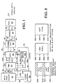
- Figure 1 is a block diagram of a typical system in which the invention might be found.
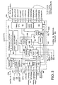
- FIG. 2 is a block diagram of a RAM buffer controller of the invention.
- Figure 3 is a diagram of the physical and logical organization of the two FIFO buffers managed by the RAM buffer controller.
- FIG. 4 is a more detailed block diagram of one embodiment of the invention.
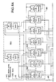
- FIGS. 5A and 5B are a more detailed block diagram of the preferred embodiment of the invention.
- Figure 6 is diagram of the organization in memory of two packets organized as a linked list.
- Figure 7 is a diagram of the organization of the fields of a typical packet.
- Figure 8 is a flow chart of the algorithm used by the invention to receive a normal packet.
- Figure 9 is a more detailed diagram of the various multiplexers and registers involved in the three receive algorithms described in the specification.
- Figure 10 is a timing diagram of the relationships of the signals involved in the algorithm for receiving normal packets.
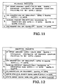
- Figure 11 is a flow chart of the algorithm for flushing packets.
- Figure 12 is a flow chart of the algorithm for aborting packets.
- Figure 13 is a timing diagram showing the process for transmitting both linked lists of packets and non-linked packets.
- Figure 14 is diagram of the memory address locations and their contents used in the example of Figure 13.
- Figure 15 is a timing diagram of the pipelined arbitration of service requests carried out by the invention.
- Figure 16 is a diagram of an asynchronous system using two systems with DMA needs each having their own clock and which share a common RAM buffer controller which runs on the clock of only one system.
- a transmission medium such as a fiber optic cable 20 is used to carry data between systems connected to the medium.
- a fiber optic transceiver 22 converts signals on the medium 20 to electrical signals in serial format, and vice versa. Signals to be transmitted on the medium 20 are sent to the fiber optic transceiver 22 on a bus 24, while signals arriving from the medium are converted to electrical signals of the proper format and output from the transceiver on a bus 26.
- An encoder/decoder 28 encodes data for transmission arriving on a bus 30 into the proper code selected for transmission on the medium 20. Data arriving from the medium 20 is decoded in the encoder/decoder 28 and output on a bus 32.
- Every local area network has a protocol. Further, every network has a topology, such as star, ring, or other topologies which may be developed in the future. To provide the flexibility in architecture to accommodate all such differences in topology and protocol, the protocol or topology-specific functions are implemented in the media access controller circuit (FORMAC) 34.
- the design of the media access controller, encoder/decoder, and transceiver are known for the various topologies and protocols which today exist. Further, they are not critical to the invention, since the RAM buffer controller of the invention is designed for use in any topology and any protocol with any type of medium. Thus, for a particular type of topology and protocol, a particular design for the media access controller will be selected. The same is true for the transceiver and for the encoder/decoder.
- This host system may be any one of a number of different types of logic systems, such as a computer, disk drive, personal computer, work station, or other peripheral. This host system may be big or small, and it may be fast or slow.
- the host system 36 has a need to transmit data packets to the other host systems on the network and to receive data packets therefrom. Because the host system may be busy doing other tasks when a receive packet arrives on the medium 20 addressed to the host system 36, it is necessary to temporarily store the received packet until the host system 36 has the opportunity to process it. Likewise, the host system 36 has a need from to time to time to transmit packets to other host systems on the network. However, the network can accommodate only one pair of transmitting and receiving host systems at any particular time. Therefore, when the host system 36 wishes to transmit a packet, it is sometimes found that its access to the medium 20 is blocked by virtue of another pair of host systems' having exclusive control of the medium 20.
- This buffer memory has an address port connected to an address bus 40 for receiving addresses which control the particular location in the buffer memory 38 from which data is retrieved or to which data is written. Data retrieved or data to be written is transmitted on or received over a data bus 46.
- a data path controller 43 is coupled to the buffer memory 38 via the data bus 46 and serves to control the data transmission to and from the buffer memory 38 on the data bus.
- the RAM buffer controller of the invention is symbolized by the block 44, which is coupled to the buffer memory 38 by the address bus 40.
- the purpose of the RAM buffer controller is to arbitrate requests for access to the buffer memory 38 by the various elements in the system of Figure 1, select one request to be honored, and to output an address pointer to the buffer memory 38 on the address bus 40 to cause the buffer memory 38 to output data from or store data in the proper address.
- the RAM buffer controller 44 maintains a set of pointer addresses stored in registers therein which can cause the buffer memory 38 to simulate the operation of two independently operating FIFO buffer memories.
- these two simulated buffers are FIFO organized, but in other embodiments, such as embodiments outside the local area network field where the RAM buffer controller is being used for stack operations, these two buffers may be LIFO organized such that the read and write pointers are managed or otherwise controlled such that a last in, first out operation is performed.
- the host system 36 can send data to the buffer memory 38 or receive data from the buffer memory 38 on a data bus 46.
- This data bus 46 is also connected to a data input of the RAM buffer controller. Further, the data bus 46 is connected to a data port of a node processor.
- the node processor 52 is a typically a microprogrammed or conventional microprocessor-based system used for overseeing the operation of the RAM buffer controller 44, the data path controller 43, and the media access controller 34.
- the node processor is coupled to these three units by an NPI bus 54.
- the main function of the node processor is to initialize the contents of various registers in the RAM buffer controller 44 and to initialize the data path controller and the media access controller 43 and 34. respectively.
- the node processor also responds to various system level and packet level interrupts. In simple systems the node processor may be the minimum state machine required for the system requirements. In complicated systems, the node processor may be a sophisticated enough machine to execute all the higher level protocols in the seven layer ISO model.
- the node processor does its work with the RAM buffer controller and the other units of the system using the NPI bus 54 and various bus handshake and instruction lines.
- the other lines in Figure 1 which have not been discussed so far are control and handshake signals which are interchanged between the units to control the direction of data transfer on the various buses, acknowledge the receipt of certain signals, signal the occurrence of various events, and otherwise control the operation of the system.
- the particular control signals which are relevant to the invention will be discussed later herein, as the need arises.
- the control lines 56 and 58 between the node processor and the host system implement a handshake which is user dependent and depends upon partitioning functions between the host and the node processor. For instance, in large systems the host may have a powerful and complex node processor 52 which is used for off loading various networking-specific chores.
- the node processor can talk to the buffer memory 38 by making a node processor service request on the control bus 101 to the RAM buffer controller and transmitting data to or receiving data from the buffer memory 38 on the data bus 46.
- a typical node processor would usually consist of a microprocessor with assorted peripheral chips for performing DMA, interrupts, etc. It would also have some local memory, and it would treat the RAM buffer controller and the data path controller as peripherals for networking functions.
- the node processor receives status information from the RAM buffer controller, the data path controller, the media access controller, and the buffer memory 38. The node processor therefore has complete control over and knowledge of the state of these units.
- the node processor runs either synchronously or asynchronously with respect to the network clock.
- the network clock is derived from the incoming data by the transceiver 22. That is, the transceiver interfaces to the medium and derives clocking information from the encoded data stream and passes this clocking signal on to the media access controller.
- the media access controller then typically converts the serial data stream to 8-bit parallel data for output on the bus 32.
- the data path controller 43 then converts the 8-bit parallel data from the media access controller and encoder/decoder to 32-bit parallel data for transmission on the data bus 46.
- the RAM buffer controller (hereafter RBC) includes request arbitration logic 62, which serves to arbitrate requests from the node processor, the data path controller (sometimes hereafter referred to as the DPC) and the host system for access by way of a DMA transfer to or from the buffer memory 38.
- DPC requests for access to the memory are made using handshake signals directly exchanged between the RBC and DPC on the bus 64 in Figure 1. These access requests by the DPC are routed by the handshake logic on line 78 to the request arbitaration logic which arbitrates the requests and acknowledges them on line 79. The acknowledge signals sent back to the DPC on bus 64 in response to the acknowledge signals on line 79 will be discussed later.
- the handshake with the DPC is performed by DPC handshake logic 66 in Figure 2.
- the signal NPRDQ to the arbitration logic 62 represents a node processor read request, while the signal NPWRRQ represents a node processor write request.
- the signal HSRDRQ represents a host system read request, and the signal HSWRRQ represents a host system write request. Again, each of the host system service requests has an acknowledge signal on the status signal bus 68.
- the DPC handshake logic 66 receives the signal DRDREQS and DRDREQA. These signals represent, respectively, a read request synchronous and a read request asynchronous from the DPC.
- the signals DRDACKS and DRDACKA respectively, represent the acknowledge signals for the aforementioned DPC read request signals.
- the signal DWRREQ represents a data path controller write request
- the signal DWRACK represents the acknowledge signal for that write request.
- RBC control logic 125 There is an RBC control logic collection of circuitry which is represented by the blocks 70, 72, 66 and 96 in Figure 2. This control logic in later figures will be collectively referred to as control logic 125.
- the RBC control logic component 70 and the RBC control logic component 72 serve to control the various multiplexers in the system (not shown in Figure 2) based on the particular mode in which the RBC is operating at any particular time via signals on bus 43. The mode that the machine is operating in is determined by the state of the control signals entering the system from all sources.
- the RBC control logic 70 also generates control signals which are transmitted to the buffer memory 38 on the bus 41. These control signals consist of the signals CSO NOT, WR NOT, and RD NOT.
- the signal CSO NOT is a chip select signal which is sent to the buffer memory 38 to select that chip, thereby causing its address and data ports to become active. This signal is low at any time that a read or write memory operation is taking place.
- the signal WR NOT tells the buffer memory that the data at its data input port coupled to the data bus 42 should be stored in the address then existing on the address bus 40.
- the signal RD NOT tells the buffer memory 38 to retrieve the data stored at the address then existing on the address bus 40 and output it onto the data bus 42.
- the addresses to the buffer memory 38 are stored in a plurality of registers symbolized by the memory address pointer block 80 in Figure 2. Depending on which access request is currently selected for service, one of these pointers is selected for output on the address bus 40. This current address is then incremented by the incrementer block 82 and fed back to the input of the pointer register selected via the bus 84. Thus, as long as that pointer register is selected, its contents will be continuously incremented according to a service request pattern established by the RBC control logic in synchronization with a byte clock signal BCLOCK on a line 89.
- the linked list mode it is necessary to input address data into certain of the registers of the RBC as pointers to the next item on the list. This address information is input on the data bus DBI 42.
- the RBC control logic causes a multiplexer 87 to select the DBI bus 42 such that its address data can be loaded into the proper registers.
- the multiplexer 87 symbolically represents a collection of input multiplexers which will be defined more specifically in later drawings herein.
- a boundary comparator 88 compares the value of the currently selected pointer on bus 90 against the end address pointers stored in the memory boundary pointer registers 92, and generates a control signal on a line 94 coupled to the RBC control logic 70 to indicate when the currently selected pointer has reached the end address of the particular FIFO of interest.
- An instruction decoder 96 decodes instructions received on an instruction bus 98 from the node processor and generates control signals on the bus 100 coupled to the RBC control logic 70 and the incrementer 82 to cause the proper events to occur to carry out an instruction.
- Table 1 below is a listing of the instructions in the RAM buffer controller instruction set and indicates what each instruction does.
- An NPI initialization bus 102 from the node processor carries initial address values established by the node processor for the starting and ending addresses of the receive and transmit FIFO buffers in the buffer memory 38. It also carries initial address values which can be loaded into most of the pointer registers in the RAM buffer controller.
- Bus interface logic 104 receives a chip select signal CSI NOT (active low as are all signals where the signal name is followed by NOT) from the node processor indicating the RAM buffer controller is selected for an operation.
- CSI NOT active low as are all signals where the signal name is followed by NOT
- Another interface signal DS NOT is active low when data on the NPI bus 102 is synchronous to the byte clock signal BCLOCK on the line 86. In such a case, the DS NOT signal behaves much like a data strobe on slave devices connected to a standard microprocessor.
- There is a signal INSTR4 in the instruction bus 98 which serves to signal whether a read or write transaction of the registers in the RAM buffer controller is requested. Each register in the RAM buffer controller can be read through a multiplexer not shown in Figure 2.
- a command and status interrupt logic 106 generates the nonmaskable interrupt signal NMINTR NOT. This signal is used for interrupting the node processor when the fatal error sets the status bit in the RBC.
- FIG. 3 there are shown both a physical and logical organization diagram of the receive and transmit FIFOs contained within the buffer memory 38.
- On the left is the physical memory organization.
- Two pointers, SAR and EAR define the starting and ending addresses, respectively, of the receive FIFO.
- Another nonoverlapping block of memory is used for the transmit FIFO, which has its starting address defined by the pointer SAX and its ending address defined by the pointer EAX.
- the receive FIFO there is a read pointer, RPR, which defines the current location for read operations by any requesting unit.
- WPR write pointer
- the write pointer, WPX defines the current location for any write operations.
- the read points, RPX defines the current location for any read operations from the transmit FIFO.
- write operations correspond to data arriving on the medium 20, which is then written into the buffer memory 38.
- Read operations for the receive FIFO correspond to accesses by the node processor or the host system to retrieve the data from the buffer memory that has arrived on the medium 20.
- write operations correspond to the host system, or possibly the node processor, writing data into the buffer memory 38 for later transmission on the medium 20.
- Read operations on the transmit FIFO correspond to the process of taking data to be transmitted out of the buffer memory 38 and converting it to the proper code to be transmitted on the medium 20.
- FIG 4 there is shown a more detailed block diagram of one embodiment of the RAM buffer controller of the invention.
- a general description of the operation of the circuitry of Figure 4 will be given, without reference to timing details at this point, to enable the reader to grasp the general operation of the system. More details will be given later on the operation of the system in connection with the description of timing diagrams detailing various modes of operation.
- the host system To transmit a packet, the host system must write the packet to be transmitted into the buffer memory 38 in Figure 1. To do this, the buffer memory 38 must be supplied with an address or addresses in the transmit FIFO in which the data is to be stored. To initiate this process, the host system will assert the signal HSWRRQ in Figure 2 to the request arbitration logic 62. There may be other service requests pending at the time that the aforementioned service request by the host system is made. It is the job of the arbitration logic to select the highest priority currently pending request for service. The priority of service requests is that DPC request have the highest priority, followed in order by node processor requests and host system requests.
- the arbitration logic 62 When the host system write request is selected for service by the arbitration logic 62, the arbitration logic transmits a select signal to a G multiplexer having inputs coupled to the outputs of the pointer storage registers in the RAM buffer controller indicating that the write pointer for the transmit buffer. WPX, is to be selected for output. This causes the output of the WPX pointer storage register to be coupled to the address bus 40 by the G multiplexer.
- the node processor will have issued a number of instructions on the instruction bus 98 to cause loading of the starting and ending addresses for at least the transmit FIFO, and the initial addresses for at least the write pointer storage register for the transmit FIFO.
- These instructions are decoded by the instruction decode logic 96 and cause the proper ones of the multiplexers A-F and H-I to select their inputs coupled to the NPI bus 102 at the time that the pointer storage register to be loaded has valid data waiting for it on the NPI bus 102.
- the node processor will load the starting address for the transmit FIFO into the SAX pointer storage register during one stage of the initialization process. Accordingly, the node processor will issue the instruction ILDSAX (see Table 1 herein), indicating that the node processor wishes to load the a SAX pointer storage register.
- the A multiplexer When this instruction is decoded, the A multiplexer will select its number 2 input (hereafter all inputs for multiplexers in the drawings will be referred to by their input number when counting from left to right) such that the NPI bus is coupled to the data input 106 for the SAX register. The proper starting address can then be loaded on the NPI bus and will be clocked into the SAX register for storage on the next BCLOCK upward transition.
- the other pointers detailed in Figure 3 are loaded by issuing one of the instructions shown in Table I to cause the particular multiplexer coupled to the data input of each pointer's storage register to select the NPI bus for coupling to the data input of the pointer storage register. The desired address data can then be loaded into the pointer storage register using the NPI bus.
- the G multiplexer When the G multiplexer receives a select signal indicating the host write request has been honored for service, this multiplexer will select the WPX register output coupled to its second input for coupling to the address output bus 40.
- the control logic 125 will also receive the select signal via the line 76 indicating which request is currently being serviced. The control logic will then generate control signals on the bus 41 to control the buffer memory.
- the control logic 125 (also sometimes referred to herein as control logic 70 after the RBC control logic portion 70 in Figure 2) will assert the signals CSO NOT and WR NOT to tell the buffer memory that a write operation is requested.
- control logic 125 will generate control signals on a bus 43, which will cause the D multiplexer to select its first input for coupling to the data input 108 of the WPX pointer storage register.
- the first input of the D multiplexer in Figure 4 is coupled to the output 83 of the incrementer circuit 82.
- the input of the incrementer circuit is coupled to the address bus 40 such that the incrementer always receives as its input the currently selected pointer address.
- the incrementer which is a conventionally designed ALU, increments the WPX pointer by 1 and transmits this incremented number to the first input of the D multiplexer.
- each address for a selected pointer will be valid for one period of the byte clock signal and will be incremented during the next period.
- control logic then causes the input multiplexers C-F for the selected pointer to select its first input coupled to the output 83 of the incrementer such that every clock cycle will cause the loading of an incremented address into the pointer storage register currently selected. This goes on for as many clock cycles as the selected pointer is selected. In the preferred embodiment, as will be described more fully below, each pointer address is valid for two clock cycles of the byte clock signal. This allows pipelined arbitration as will be described in more detail below.
- the control logic when the WPX pointer is selected for output, causes the D multiplexer to select its number 4 input during the two clock cycles of the bus transfer period on the data bus for one word, and causes the D multiplexer to select its number 1 input at the end of the second clock cycle of the service period so that the WPX pointer will be incremented by 1 for the next two cycle service period if the WPX pointer is still selected during the next service period. This process continues until all the words of the packet to be stored in the buffer memory by the host system 36 are so stored.
- the select signal from the arbitration logic 62 to the G multiplexer causes that multiplexer to select the WPX pointer and output it on the address bus 40.
- a comparator 88 has one of its comparison inputs coupled via the bus 90 to the address bus 40. The other input of this comparator 88 is coupled to the output of the J multiplexer, which has as its inputs the end address pointers for both the transmit and receive FIFO buffers. These addresses have been previously loaded by the node processor 52 in the EAX and EAR pointer storage registers.
- This loading was accomplished as described above by causing the H multiplexer to select its number 2 input coupled to the NPI bus after issuance of a load EAX instruction, and by causing the I multiplexer to select its number 1 input after issuance of a load EAR instruction by the node processor.
- the control logic which will be collectively referred to by reference number 125 in Figure 4, causes the J multiplexer to select its number 1 input for coupling to the B input of the comparator 88.
- the comparator 88 compares the selected pointer value, in this case WPX, to the end address for the transmit buffer.
- the comparator 88 outputs a signal on a line 94 coupled to the control logic 125 which indicates whether the selected pointer is equal or not equal to the appropriate end address for the buffer to which the selected pointer pertains, i.e., the transmit buffer in this example.
- the control logic allows incrementing of the selected pointer to proceed until such time as the signal on line 94 indicate that the selected pointer is equal to the end address.
- the control logic 125 causes the input multiplexer for the selected pointer, in this case the D multiplexer, to select the input coupled to the output of the appropriate starting address pointer storage register, i.e., the number 2 input for the D multiplexer.
- the WPX pointer will be continuously incremented as long as it is selected until such time as it equals the end address for the transmit buffer. At that time, the signal on the line 94 will change states, and the control logic 125 will cause the D multiplexer to select its number 2 input, thereby loading the starting address for the transmit buffer from the SAX pointer storage register into the WPX pointer storage register. If the WPX pointer continues to be selected for further transactions, incrementing will continue from the starting address of the transmit buffer.
- the data path controller and media access controller modules will be signaled that there is a packet ready for transmission on the media 20, said packet having been loaded into the buffer memory 38 by the host system or by the node processor.
- the data path controller 43 will assert a service request requesting that data be read from the buffer memory 38.
- This request from the data path controller takes the form of assertion of the signal DRDREQS or DRDREQA in Figure 2.
- These two signals stand for data path controller read request synchronous and data path controller read request asynchronous.
- the assertion of a data path controller read request causes the control logic 125 to generate the proper select signal to the G multiplexer to select the RPX pointer. This pointer is the read pointer for the transmit buffer.
- the control logic 125 also causes the C multiplexer to select the number 3 input during the two cycles of the service request so as to maintain the RPX pointer constant at its then existing value. At the end of the second cycle of the service request, the control logic 125 causes the C multiplexer to select its number 1 input coupled to the output of the incrementer 82 to allow the RPX pointer to be incremented. As long as the RPX pointer is selected, it will be maintained constant during two clock cycles and will be incremented at the end of every service cycle. That is, the address or RPX pointer output on address bus 40 causes the buffer memory 38 to retrieve the data at the specified address and output it on the data bus 42. The data path controller and media access controller circuitry then processes this data and, with the help of the encoder/decoder 28 and transceiver 22, transmits the data on the medium 20.
- the RPX pointer is constantly compared to the end address for the transmit buffer by the comparator 88 while RPX is selected. If at any time RPX become equal to EAX, the signal on line 94 changes state, thereby causing the control logic 125 to generate a select signal to the C multiplexer. This select signal causes the C multiplexer to select its number 4 input, thereby loading the starting address for the transmit buffer into the RPX pointer storage register from the SAX pointer storage register.
- the data path controller When data arrives on the medium 20, the data path controller will assert a write request in the form of activation of the signal DWRREQ. This causes the control logic 125 to generate a select signal to the G multiplexer to select its number 4 input, thereby outputting the WPR pointer on the address bus 40. As before, the control logic 125 will cause the F multiplexer to select its number 3 input for the two clock cycles of the transaction time for one word of the incoming data. At the end of the two cycle service period, the control logic 125 will cause the F multiplexer to select its number 1 input, thereby allowing the WPR pointer to be incremented at the start of the two clock cycles representing the next WPR address and service period.
- the WPR pointer address on the address bus 40 is compared by the comparator 88 to an end address for the appropriate buffer, i.e., the receive buffer.
- the control logic will order the J multiplexer to select its number 2 input such that the end address for the receive buffer is coupled to the B input of the comparator 88.
- a signal on the line 94 will change states, thereby causing the control logic 125 to generate a select signal to the F multiplexer, causing it to select its number 4 input, thereby loading the starting address for the receiver buffer into the WPR pointer storage register.
- the host system 36 may, at its leisure, assert a read request signal to the arbitration logic 62.
- This event would take the form of assertion of the signal HSRDRQ on bus 103 in Figure 2. If this is the highest priority request then pending, the arbitration logic 62 would generate a select signal which would cause the G multiplexer to select its number 3 input, thereby outputting the RPR pointer address on the address bus 40.
- the control logic 125 would be notified on the control line 76 of the winning request and would know that a read transaction was requested. The control logic 125 would then generate the proper control signals on the bus 41 to the buffer memory to select the buffer memory and cause it to perform a read transaction.
- the buffer memory would then access the data stored in the address pointed to by the address on bus 40 and output the resulting data on the data bus 46.
- the host system could then read the data on the data bus 46 and do with it whatever needed to be done.
- the control logic 125 would also generate the proper control signals to cause the E multiplexer to select its number 3 input during the two cycles of the read transaction for each word and to select its number 1 input at the end of each service period to allow the RPR pointer storage register contents to be incremented by one.
- the comparison of the RPR pointer to the end address for the receive buffer EAR occurs as described above for the other pointers. If the RPR pointer becomes equal to EAR, the control logic 125 orders the E multiplexer to select its number 4 input, thereby loading the starting address for the receive buffer into the RPR pointer. As in the case of the other pointers, the E multiplexer selects is number 3 input for the two cycles of the service period, and it selects its number 1 input at the end of the service period to allow the RPR pointer to be incremented.
- the invention utilizes a series of input multiplexers denoted by the letters C-F in Figure 4, each of which has one input which is coupled to the NPI bus 102.
- the output of the incrementer 82 is coupled to another input of each of these input multiplexers. Because the NPI bus and the output of the incrementer on the bus 83 do not have to pass collectively through a common multiplexer with its output coupled to an input of each of the input multiplexers, it is possible to initialize any of the pointer storage registers from the NPI bus while selecting another pointer for output on the address bus 40.
- any particular pointer address storage register is selected for output of its contents by the G multiplexer onto the address bus 40, then any of the other pointer storage registers not so selected may be initialized through the NPI bus 102 without interfering with the selection and incrementation of the pointer address in the selected pointer storage register. This is done by issuing the appropriate load instruction on the instruction bus 98 thereby causing the control logic 125 to cause the appropriate input multiplexer to select its input coupled to the NPI bus. If the node processor attempts to initialize the pointer currently selected, an error condition results and an interrupt is generated.
- FIG 4 there is a pointer storage register designated MAR which is used to store a pointer address (also referred to as an address pointer) for servicing node processor read or write requests.
- the random access pointer MAR can be initialized by the NPI bus in the same manner as any of the other pointers.
- the node processor issues a load MAR instruction which is decoded and causes the control logic 125 to send a select signal to the K multiplexer causing it to select its number 2 input to couple the NPI bus to the data input of the MAR pointer storage register.
- the desired address can then be loaded on the NPI bus. and it will be stored in the MAR register.
- the node processor may assert a service request in the form of activating one of the signals NPRDQ or NPWRRQ in Figure 2. If either of these lines is activated, the request arbitration logic 62 causes the G multiplexer to select its number 5 input, thereby outputing the MAR pointer on the address bus 40. Depending on which of the node processor signals is activated, the control logic 125 generates the proper control signals on the bus 41 to cause the buffer memory 38 to either read data stored at the address on address bus 40 and output it on the data bus 46, or input data from the data bus 46 and store it in the address existing on the address bus 40.
- the comparator 88 compares it to the ending address for the transmit buffer or for the receive buffer, but the output signal of the comparator on line 94 is ignored by the control logic 125.
- the random access pointer is not limited by any address limitations of the FIFO or LIFO buffers managed by the RAM buffer controller. That is, the random access pointer may be set to any address within the physical address space of the buffer memory 38.
- Any node processor service request has the second highest priority in arbitration, and is serviced only if a data path controller request is not present simultaneously.
- There is a command register in the control logic 125 which contains a command bit called CENNPRQ. This command bit can be set or cleared to enable or disable the node processor requests. It would normally be set to disable node processor requests while a DPC request was being serviced.
- the control logic 125 When a node processor request is being serviced, the control logic 125 generates an acknowledge signal which is active for the duration of the transfer. There is a separate acknowledge signal for a node processor read request and another acknowledge signal for a node processor write request.
- the node processor inputs data from the buffer memory on the data bus 46 at its data port in Figure 1 and the same data port is used for outputting data to be stored in the buffer memory 38. Since the random access pointer register is not subject to reloading with a starting address upon reading an ending address of either the transmit or receive FIFOs, the random access pointer MAR will be continuously incremented during the entire time it is selected until it reaches its highest value of all ones. At that point it will be reset to a value of all zeros.
- Node processor service requests are typically used by the node processor to do block DMA transfers of data to or from the memory.
- the acknowledge signals for the node processor service request are output from the control logic 125 on a bus 68 in Figure 4.
- a status signal NPPND is provided on the bus 68 to indicate to the node processor whether there are any requests pending to be serviced.
- a host system service request is being serviced, one of two acknowledge signals on the bus 68 dedicated to acknowledging host service requests is active.
- There is a separate acknowledge signal for a host read transaction and another acknowledge signal for a host write transaction. Both types of host requests have equal priority and are serviced alternately.
- Two command bits are provided to independently enable or disable the host system read request and host system write request input ports. These command bits are resident in a command register (not shown) located in the control logic 125.
- the random access pointer MAR is used by the node processor to look at headers of packets after a packet has been received. That is, the random access pointer can be used as part of the mechanism used by the node processor to filter out packets that are not addressed to the host system 36 or which have been received but in which CRC errors have been detected.
- the node processor has a way of preventing the incrementer 82 from incrementing the MAR pointer such that this pointer can be used for a read-modify-write cycle on buffer memory 38, which otherwise would not support this type of data transaction.
- the node processor would send an instruction via the instruction bus 98 in Figure 2 to the instruction decoder 96. This instruction could be one of the reserved instructions in Table 1.
- the instruction could be encoded and a signal transmitted on the line 100/101 to the incrementer 82 to prevent it from incrementing.
- the node processor could use the initial address of the MAR pointer and assert a read request.
- the data output from the buffer memory could then be input by the node processor 52 and modified.
- the node processor could then assert a write request and transmit a do not increment instruction to the RAM buffer controller. Then the node processor would issue a write request and then write the modified data to the same memory address from which it was read.
- the do not increment signal on line 101 in Figure 4 is used to block the carry-in input to the incrementer ALU to block incrementation.
- the node processor can assert its DMA requests either by asserting one of the signals NPRDQ or NPWRRQ on the bus 101 or by issuing one of the software instructions noted above.
- the node processor cannot assert both a hardware request and a software request at the same time since the MAR is selected by the control logic for any node processor service request and inconsistencies could develop.
- the foregoing instructions may be used to implement a read-modify-write sequence as follows.
- the node processor issues instruction INPRDNI to read the memory location pointed to by the MAR but the MAR is not incremented.
- the data is then modified, and the node processor issues instruction INPWRWI to write the modified data back into the same memory location which is then pointed to by the MAR.
- the MAR is then incremented during the a portion of this write access.
- the foregoing instructions may also be used to implement a write-verify sequence as follows.
- the node processor issues the instruction INPWRNI to write data into the location pointed to by the MAR, and the MAR is not incremented. Thereafter, the node processor issues the instruction INPRDWI to read the contents of the location just written and the MAR contents are incremented during this read transaction.
- Each packet has a byte called a descriptor at the beginning of the packet followed by one or more bytes of data.
- the descriptor byte has transmit status and length information stored therein.
- Each packet is followed by a pointer byte which contains the starting address of the next member of the list to be transmitted.
- the pointer byte 130 is the pointer byte for packet number 1, while the pointer byte 132 is the pointer for packet number 2.
- the descriptor 134 is the descriptor for packet number 2. If packet number 2 were to be transmitted following the transmission of packet number 1, the pointer 130 would point to the address of the descriptor 134.
- the circuitry of the DPC contains a circuit to identify when a word read from the buffer memory 38 is a pointer address.
- the pointer 130 When the pointer 130 is read at the end of transmission of packet number 1, the contents of pointer 130 would be loaded in the RAM buffer controller as the new value for the RPX read pointer for the transmit buffer.
- the address of the descriptor 134 On the next read request for access to the transmit buffer, the address of the descriptor 134 would be found in the RPX pointer storage register and transmission of packet number 2 would begin from that point. If, on the other hand, packet number 2 was to be transmitted first and packet number 1 was to be transmitted following the transmission of packet number 2, then the contents of pointer 132 would be the address of the descriptor 128 for packet number 1.
- descriptor 132 when descriptor 132 was read, its address contents would be loaded into the RPX pointer storage register, and upon a read request for the transmit buffer again occurring, transmission of packet number 1 would start at the location of the descriptor 128
- FIG. 5A and 5B there is shown a block diagram of the RAM buffer controller in its preferred embodiment.
- the portion of the RAM buffer control circuitry which supports the linked-list transmission of packets is the data bus 42 and its connection to one of the inputs of the input multiplexer controlling the data inputs of the read pointer for the transmit buffer.
- there are two read pointer storage register for the transmit buffer designated, respectively, RPXS and RPXA.
- the data bus 42 is coupled to one input of each input multiplexer controlling the data inputs for the RPXS and RPXA pointer storage registers.
- the data path controller When the data path controller is performing read operations from the transmit buffer during linked-list transmit mode, it detects the reading of pointer addresses such as pointers 130 and 132. When such a pointer is read by the data path controller 43 in Figure 1, the data path controller asserts an interface signal to the RAM buffer controller called LDRPXS or LDRPXA, depending upon which pointer storage register is assigned to the particular linked list being transmitted. When the control logic detects the activation of this signal on bus 64, it signals the appropriate one of the input multiplexers C or L to select the input coupled to the DBI bus 42. Because at that time the contents of the pointer will be resident on the DBI bus 42, the pointer address is loaded into the appropriate one of the RPXA or RPXS pointer storage registers on the next upward transition of the BCLOCK signal.
- the embodiment of Figures 5A and 5B shows two full/empty comparators 140 and 142.
- the comparator 140 has one compare input coupled to the output of the RPXS pointer and the other input coupled to the output of the WPX pointer.
- the comparator 140 serves to compare these two pointers and generate a transmit buffer full/empty signal called RPXEQWPX, which is coupled to the control logic 125.
- the signal RPXEQWPX become active when the read pointer and the write pointer for the transmit buffer become equal. This condition indicates either that the transmit buffer is full or that it is empty.
- the control logic 125 determines which case is true by examining the last transaction which occurred in the service request prior to the cycle during which the signal RPXEQWPX became active. If the last transaction before the two pointers became equal was a read, the transmit FIFO is empty. If the last transaction before the two pointers became equal was a write, then the transmit FIFO is full.
- the comparator 142 acts in a similar manner as the comparator 140 in monitoring the full/empty status of the receive FIFO.
- the comparator 142 has one compare input coupled to the output of the RPR register, and another compare input coupled to the output of the WPR register.
- the comparator 142 activates the signal RPREQWPR coupled to the control logic 125.
- the rule for determining whether the receive FIFO is full or empty is the same as the rule for the transmit FIFO.
- the control logic sends a select signal to the H multiplexer causing it to select its number 2 input coupled to this bus 150 such that the contents of the RPXS pointer storage register is loaded into the EAX pointer storage register on the next clock uptick.
- the control logic 125 sends a select signal to the H multiplexer causing it to select its input number 3, which is coupled to the output of the EAX storage register, such that the contents of the EAX pointer storage register is maintained constant.
- the node processor can read the contents of any pointer storage register in the RAM buffer controller of Figures 5A and 5B by sending a read instruction for the particular pointer storage register of interest to the control logic 125 over the instruction bus 98.
- the node processor may send a read EAX instruction to the control logic 125 which will be decoded and will cause the read multiplexer 152 to select its input coupled to the output of the EAX pointer storage register.
- the data in the EAX pointer storage register may then be reloaded into the RPXS pointer storage register via the NPI bus 102.
- the data path controller can then again assert a read request for access to the transmit buffer such that RPXS is selected by the G multiplexer for output on the address bus 40. Transmission will then resume with the packet which was interrupted by the ring recovery situation.
- the node processor in a ring recovery situation, does not restore the contents of the EAX pointer storage register into the RPXS pointer storage register. Instead, it uses the contents of the EAX pointer storage register as an indication of how many packets were successfully transmitted before the interruption. The node processor then figures out which packet must be the first one sent from the linked-list transmission that was interrupted, i.e., it figures out and loads into RPX the address of the descriptor of the first packet which was not successfully transmitted.
- Figure 7 shows a typical data structure for a packet transmitted on the medium 20 in Figure 1.
- a first field or group of fields will hold control information, and these fields will be followed by a destination address indicating the particular host system to which the data portion of the packet is addressed.
- the source address follows the destination address and gives the network address of the originating host system which transmitted the data. Following the source address there will one or more bytes of data comprising the subject matter of the packet followed by one or more bytes of CRC data which provide check bits to improve the reliability of the data.
- all node processors on the network begin copying the incoming data into the buffer memory.
- These ten or more control bytes must be copied into the buffer memory 38 in case the destination address proves to be the address of the particular host system at that node. If, however, after the control bytes have been stored, the destination address arrives and is compared by the node processor to the address of the host system at that node and the two do not match, then it is necessary to flush all the control bytes and other bytes received in that packet so as not to waste memory space with unneeded data.
- the mechanism in the preferred embodiment to do this flushing is the shadow write pointer storage register, designated SWPR in Figure 5A.
- This shadow write pointer has an M multiplexer which controls the data inputs of the SWPR pointer storage register.
- This M multiplexer has one of its inputs coupled to the output of the WPR storage register and has the other input coupled to the output of the SWPR pointer storage register.
- the output of the SWPR pointer storage register is also coupled to one of the inputs of the F multiplexer, which controls the input of the WPR pointer storage register.
- the concept of packet flushing involves saving the contents of the WPR into the SWPR pointer storage register at the beginning of reception of each packet.
- the SWPR storage register stores the contents of the WPR pointer storage register as it existed at the time when packet reception commenced. Then, if it is necessary to flush the packet, the contents of the SWPR register are restored to the WPR pointer storage register, thereby resetting it to the position that it had at the beginning of the reception of the faulty packet.
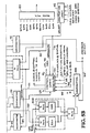
- Figure 8 is a flow chart of the algorithm for receipt of a normal packet.
- Figure 9 is a more detailed block diagram showing the various multiplexer select signals for the F and M multiplexers controlling the WPR pointer storage register and SWPR pointer storage register. These select signals are manipulated by the control logic to implement the algorithm of Figure 8 in accordance with the timing diagram shown in Figure 10.
- Figure 10 relates the timing relationship of all of these select signals shown in Figure 9 to implement the algorithm of Figure 8 for reception of a normal data packet.
- the first step in receiving a normal data packet is to initialize the WPR pointer storage register to a valid address.
- the control logic 125 asserts the signal LDNPWPR at 170 in Figure 10. This causes the F multiplexer to select its B input for application to the data inputs of the WPR pointer storage register.
- the B input is connected to the NPI bus, which will have previously been driven by the node processor to an address state of an address in which the node processor wishes the first word of the incoming packet to be stored. If packets are to be stored contiguously in memory, the initialization step may be omitted after the first initialization occurred, since the WPR pointer storage register will be continuously incremented until it reaches the end address of the receive FIFO. After a sufficient amount of time for the loading of the WPR register to occur, the signal LDNPWPR is deactivated at 172.
- the WPR pointer storage register must then be held at the initialization value. Therefore, the control logic asserts the signal HLDWPR at 174 in Figure 10.
- the signal HLDWPR remains asserted for as many clock cycles as occur prior to the beginning of reception of an incoming packet. In other words, reception of a packet does not actually begin until step 2 in Figures 8 and 10.
- the beginning of receipt of a packet is signaled by the assertion of a signal BRCVPKT on bus 64 in Figure 2 from the data path controller.
- BRCVPKT Upon the assertion of the signal BRCVPKT, several things happen.
- the contents of the WPR pointer storage register are loaded into the shadow write storage register, SWPR, and the WPR pointer storage register is incremented by one, thereby skipping the first location after saving the contents of the WPR.
- the control logic deactivates the select signal HLDWPR, thereby deselecting the D input of the F multiplexer.
- the WPR output data will be fed back into its D input such that every uptick of the clock signal BCLOCK will reload the WPR with its presently existing data, thereby holding it at a constant address.
- the control logic at t1 asserts the signal LDWPSWPR at 178 in Figure 10.
- the control logic deactivates the signal HLDSWPR, which is normally active at all times except times when the SWPR pointer storage register is being loaded with new data.
- the select signal LDWPSWPR causes the M multiplexer in Figure 9 to select its input A. This selects the output of the WPR pointer storage register for application to the D input of the SWPR pointer storage register. Upon the next occurrence of a BCLOCK upward transition, the transfer will occur.
- the control logic at time t1 in Figure 10 asserts the select signal LDINCWPR, as shown at 182 in Figure 10.
- the control logic at time t1 will assert the signal SELWPR.
- This causes the G multiplexer to select the input coupled to the WPR pointer storage register output for output on the address bus 40.
- the incrementer 82 then adds one to the contents of the WPR pointer storage register and outputs the incremented value on the bus 83.
- the first data packet word arrives.
- the occurrence of this event is signaled by the assertion of the signal DWRREQ in Figure 2 from the data path controller 43.
- the WPR pointer storage register was placed in the hold status by assertion of the signal HLDWPR, as shown at 186 in Figure 10. This caused the F multiplexer to select its D input for application to the data input of the WPR pointer storage register.
- control logic asserts the signal LDINCWPR, as shown at 188, and asserts the signal SELWPR, as shown at 190.
- control logic asserts the signal CSO NOT, as shown at 192, to enable the buffer memory 38, and the control logic asserts the signal WR NOT at 194 to inform the buffer memory that a write transaction is requested.
- the assertion of SELWPR causes the current content of the write pointer storage register, WPR, to be output on the address bus 40.
- the first word of the received packet to be written into the buffer memory at the address on bus 40 has previously or simultaneously been placed on the data bus 46 by the data path controller 43.
- the buffer memory then writes the data on the data bus into the address pointed to by the current contents of the WPR pointer storage register.
- the simultaneous assertion of LDINCWPR causes the contents of the WPR pointer storage register to be incremented by one on the next upward transition of the BCLOCK signal by virtue of the incrementer having the WPR pointer applied to its inputs and the incremented value applied to the C input of the F multiplexer.
- the data path controller When the data path controller and the other circuitry in the system of Figure 1 detect the end of the incoming packet, the data path controller asserts the signal ERCVPKT on bus 64 in Figure 2. This is the signal which causes the exchange of pointer register contents symbolized by step 4 in Figure 8 to occur.
- the contents of the shadow write pointer storage register are loaded into the WPR pointer storage register and the contents of the WPR pointer storage register are loaded into the shadow write pointer storage register simultaneously.
- the control logic 125 implements this swap by asserting and deasserting various signals at time t7 in Figure 10.
- the select signal LDSWWPR is asserted, causing the F multiplexer to select its E input for application to the data input of the SWPR pointer storage register.
- the E input of the F multiplexer is coupled to the output of the SWPR pointer storage register. Therefore, this causes loading of the then existing contents of the SWPR register into the WPR pointer storage register.
- the control logic deasserts the select signal HLDWPR as shown at 198 to release the hold on the contents of the WPR pointer storage register.
- the control logic also asserts the select signal LDWPSWPR, as shown at 200, to cause the M multiplexer to select its A input for application to the data input of the SWPR pointer storage register.
- the A input of the M multiplexer is coupled to the output of the WPR pointer storage register, and therefore, the contents of the WPR pointer storage register are loaded into the SWPR register upon the next upper transition of the BCLOCK signal.
- the control logic also deactivates the select signal HLDSWPR at that time to allow the swap to occur.
- the contents of the WPR pointer storage register will have been swapped with the contents of the SWPR pointer storage register.
- the contents of the WPR pointer storage register are now equal to the address that the WPR register stored at the beginning of reception of the packet in step 2 of Figure 8 before the WPR register was incremented in step 2. That is, if a packet occupies address locations 1-100 in memory, then the data words in the packet will occupy locations 2-100 and the WPR pointer storage register will contain an address pointing to storage location 1 upon completion of step 4 in Figure 8. In other words, location 1 is the memory location skipped by the incrementation that occurred in step 2 of Figure 8.
- location 1 is the location in which the status and length information for the packet is stored. It is useful in local area network design to store status and length information with each packet. This information indicates whether or not it is a valid packet and the length of the packet in terms of the number of memory locations consumed by the packet. It is useful to put this status and length information at the beginning of the packet rather than at the end of the packet. The reason for this is that it simplifies the software overhead in the node processor, because the node processor knows exactly where to look for the status and length information in each packet without having to know how long the packet is, which it would have to know if the status and length information were stored at the end of the packet.
- Step 5 in Figure 8 represents the step of writing the status and length information in the first memory location of the packet. In the hypothetical example just given, this would mean the status and length location would be written into memory location 1. This occurs at time t9 in Figure 10.
- Step 5 is implemented by asserting the signal SELWPR at 204, which outputs the current contents of the WPR to the address bus 40. Also asserted are the signals CSO NOT and WR NOT. These two signals activate the buffer memory and tell it that a write transaction is about to occur. The buffer memory then writes into the pointed to location the data on the data bus, which, at time t9, is the status and length information.
- Step 6 in Figure 8 is implemented in Figure 10 by the assertion of the signal LDSWWPR at 206 and the deactivation of the signal HLDWPR at 208.
- the events at 206 and 208 in Figure 10 cause the F multiplexer to select the D input, thereby loading the contents of the SWPR back into the WPR pointer storage register.
- the WPR pointer storage register would now be pointing to address location 101.
- step 7 a zero bit is written into a specific bit location of the memory location just following the last word in the data packet just received, and the WPR pointer storage register is held constant at that pointer address value. That is, in the hypothetical example, step 7 represents the step of writing a zero into a particular bit of memory location 101 and holding the WPR pointer at 101. The reason that this is done is to cause a zero bit to be written into a specific bit of the memory location just following the data packet. When the node processor or host system is reading data out of the receive buffer, and it reads locations 101, it will see this particular bit set at zero. This will tell the node processor or host system that all that follows is not a valid packet.
- Valid packets are designated by writing a one into the designated bit during step 5 of Figure 8 when the status and length information is written into the first memory location of the packet.
- Step 7 is represented at t10 in Figure 10 by the assertion of the signal HLDWPR at 210 to hold the WPR content steady by forcing the F multiplexer to select its D input and by continued selection of the WPR output by the G multiplexer by continued assertion of the signal SELWPR at 212.
- Writing of the zero bit, as required by step 7 of Figure 8, is accomplished by the continued assertion of the signals CSO NOT and WR NOT at 214 and 216 between times t10 and t11.
- Steps 1 through 3 of this algorithm are identical to steps 1 through 3 of the algorithm for receiving a normal packet shown in Figure 8.
- the DPC Upon detection of the fact that a packet is not addressed to the host system at the particular node or that a CRC error has occurred, the DPC asserts a signal FSHRCVP, meaning flush this packet.
- This signal, FSHRCVP is one of the interface signals to the RBC control logic 72 in Figure 2, which comes from the DPC over the bus 64. When this signal is asserted, the contents of the SWPR pointer storage register are loaded into the WPR pointer storage register.
- step 4 in Figure 11 would restore the WPR pointer address to memory address 1. Since no status and length recording step will have been performed in the algorithm at the time that FSHRCVP is asserted, the status bit at memory location 1 will still be a zero from the previous packet reception. That is, if the previous packet received was normal, the system in step 7 of the algorithm to receive normal packets will have written a zero bit into the memory location following the last word in the previous packet. In the hypothetical example, this assumes that the previous packet's last word will be stored in memory location 0. This zero status bit will indicate to the node processor or host system that all the data which is in a memory location following memory location 1 is invalid data thereby effectively flushing the packet.
- the algorithm of Figure 12 is the process which the RAM buffer controller implements in the event that a packet is to be aborted. Steps 1 through 3 of the aborted packet algorithm are the same as the first three steps of the algorithm for receiving normal packets as previously described, and will not be described again here.
- the WPR pointer storage register is reset to the memory location at which it pointed at the time that packet reception began, and status and length information is written. This transaction is symbolized by step 4 in Figure 12 wherein the contents of the SWPR pointer storage register are reloaded into the WPR pointer storage register. Because in step 2 the contents of the WPR pointer storage register were saved into SWPR, this restores WPR to the pointer address it had at the time when packet reception began. In the hypothetical example given above, the WPR pointer storage register would then be pointing to address location 1.
- Step 5 of Figure 12 represents the step of writing the status and length information for the aborted packet.
- the control logic would assert the select signal SELWRP, forcing the G multiplexer to select the output of the WPR register. Further, the control logic would assert the chip select signal and the write signal to the buffer memory to enable the buffer memory and tell it to write the data then existing on the data bus 46 into the memory pointed to by the current contents of the WPR, i.e., address location 1.
- the node processor, or DPC will have loaded the status and length information on the data bus prior to or simultaneously with the chip select and write signals to the buffer memory.
- Step 5 also represents the process of incrementing the WRP pointer storage register by one. This is done in the same manner as described above with reference to Figure 10.
- Step 6 of Figure 12 is the final step in the aborted packet algorithm. This step involves writing a zero status bit into the predetermined bit in the memory location following the status and length information for the aborted packet. In the hypothetical example, this zero status bit would be written into memory address location 2. The manner in which this is done is identical to step 7 in the algorithm represented by Figure 8.
- FIG. 13 there is shown a timing diagram for the sequence of events which occurs during both linked-list transmission and nonlinked-list transmission.
- Nonlinked-list transmission occurs as follows. To load the buffer memory with the packet to be transmitted, the host system asserts a host system write request in the form of assertion of the signal HSWRRQ, shown at 220. This assertion is sensed by the priority arbitration logic 62 in Figure 2 and acknowledged by assertion of the signal HSWRACK at 222. This acknowledgement signal is sent back to the host system via the status bus 68 in Figure 2.
- a hypothetical example will be used to illustrate the operation of the system, as shown in Figure 13. In this hypothetical, the contents of the WPX pointer storage register at the outset of the transmission is zero, as are the contents of the RPX pointer storage register.
- the G multiplexer is ordered by the control logic to select the output of the WPX pointer storage register. This causes the zero stored in the WPX pointer storage register to be applied to the input of the incrementer 82.
- the incrementer then outputs a one on line 83.
- the host system write request acknowledge signal lasts for two clock cycles, i.e., between the times t2 and t4 in Figure 13. In other embodiments, one clock cycle might be used, or more than two clock cycles might be used.
- the incrementer output line 83 stays constant at one, however, from the time of the transition 222 to the transition 224 at t4.
- the transition 224 causes the control logic 125 in Figure 4 to cause the D multiplexer in Figure 4 to select its number 1 input, thereby loading the one at the incrementer output into the WPX pointer storage register.
- the first word of the packet to be transmitted was loaded into the buffer memory at address location zero.
- the host system asserts another write request, as shown at 226. This causes an acknowledgement signal by the host system by assertion of the signal HSWRACK, as shown at 228.
- the transition at 228 causes the arbitration logic 62 to issue a select signal to the G multiplexer which selects the output of the WPX pointer storage register for connection to the address bus 40. This applies the current contents of WPX to the incrementer input, which then increments the one currently residing in the WPX register to a two, and outputs it on line 83.
- the second word to be transmitted is loaded by the host system into the buffer memory 38 at address one via the data bus 46.
- the host system asserts another write request, as shown at 230.
- the data path controller asserts a read request by activating the signal DRDREQS on bus 64 in Figure 2. This assertion is shown at 232 in Figure 13.
- the control logic 125 in Figure 4 blocks requests from the node processor or host and awards priority to the data path controller, because the data path controller always has the highest priority. Basically, the process that is occurring here is the host system is trying to fill up the transmit buffer with words from a packet that it wishes to transmit. Substantially simultaneously, the data path controller is starting to empty words from the buffer memory and transmit them out on the medium.
- the award of priority to the data path controller is shown by the assertion of the data path controller read request acknowledge signal, DRDACKS, as shown at 234 in Figure 13.
- the award of priority to the data path controller precludes sending an acknowledgement signal to the host system to acknowledge its write request shown at 230. This is shown by the absence of assertion of the acknowledge signal HSWRACK between times t8 and t9, as shown at 236.
- the assertion of the data path controller acknowledge signal, DRDACKS, at 234 causes the control logic to send a select signal to the G multiplexer, causing it to select the contents of the RPX pointer storage register for output on the address bus 40. This supplied the current contents of the RPX pointer storage register on address bus 40 at time t8 to the buffer memory 38.
- a zero pointer address would be supplied to the buffer memory for the DPC read operation commencing at time t8 in the hypothetical example used here. Accordingly, the buffer memory would output the contents of the zero address location between times t8 and t10.
- Figure 14 shows a hypothetical set of memory addresses and their contents. Accordingly, a 100 would be placed on the data bus in response to the DPC read request corresponding to the word written into the memory by the host system between times t2 and t4. Also the RPX value of zero would be applied to the input of the incrementer, which would then increment it and output a one on line 83 at time t8.
- the deactivation of the DPC acknowledge signal at time t10 at 236 causes the C multiplexer in Figure 4 to select its input coupled to the output of the incrementer for coupling to the data input of the RPX pointer storage register. This loads the one at the output of the incrementer into the RPX pointer storage register, thereby incrementing this pointer from zero to one.
- the arbitration logic 62 Upon completion of servicing of the DPC read request at time t10, the arbitration logic 62 acknowledge the pending host system write request, asserted at time t7. This is done as shown at 238 in Figure 13 by asserting the host system write acknowledge signal HSWRACK at time t10. The assertion at 238 causes the G multiplexer to once again select the contents of the WPX pointer storage register for output on the address bus. The incrementer then takes the current contents of the WPX pointer storage register at address two and increments it to address number three.
- the signal HSWRACK is deactivated, which causes the control logic to order the D multiplexer to select its number 1 input coupled to the output of the incrementer, thereby loading the three at the output of the incrementer as the new incremented pointer address for the WPX pointer storage register.
- the data path controller asserts another read request, as shown at 242.
- This DPC read request is acknowledged at time t12 by the arbitration logic 62, as shown by the assertion of the signal DRDACKS at 244.
- the assertion at 244 causes the G multiplexer to again select the contents of the RPX pointer storage register for output on the address bus 40, thereby supplying the one currently stored as the RPX pointer to the input of the incrementer.
- the incrementer increments the pointer address one to pointer address two, and applies it to the output line 83.
- control logic Upon completion of the DPC read service request at time t14 as shown at 246, the control logic causes the multiplexer in Figure 4 to select its number 1 input coupled to the output of the incrementer, thereby loading the address two pointer value into the RPX pointer storage register. This completes the illustration of the nonlinked-list transmission of words from the buffer memory. This example extends from time t0 to t14 in Figure 13.
- the data path controller asserts another read request as shown at 248. This is acknowledged by the control logic 125by asserting the signal DRDACKS at time t15, as shown at 250. As described earlier, the assertion of the DRDACKS signal at time t15 causes the current contents of the RPX pointer storage register, address two, to be applied to the input of the incrementer and incremented to a value of address three.
- Figure 14 shows a hypothetical example of several memory locations having addresses 0-5 and showing the contents of these memory location.
- Figure 13 shows the data on the data bus during read cycles on the line entitled "Memory Contents on DBI".
- the first read transfer from the buffer memory 38 occurs between times t8 and t10. At that time the RPX pointer address is zero, and the contents of the zero address, a 100 value, is placed on the DBI bus. The next read cycle occurs between times t12 and t14. At that time, the RPX pointer value is one, and the contents of address one are placed on the DBI bus. Thus, a 200 value is found on the DBI bus between times t12 and t14. The next read cycle occurs between times t15 and t17. At that time the RPX pointer is on address location two, so the data on the DBI bus represents a value 300.
- the deactivation of the signal DRDACKS at time t17 causes the C multiplexer in Figure 4 to select its number 1 input, thereby loading the output of the incrementer, a value of three, into the RPX pointer storage register, a shown at 252 in Figure 13.
- the data path controller again asserts a read request, as shown at 254.
- This read request is acknowledged at 256 and time t18. As described before, this causes the RPX pointer to be selected for output by the G multiplexer on the address bus 40, thereby outputting an address of three to the buffer memory.
- This address value of three is incremented by the incrementer 82 and applied to the first input of the C multiplexer by the line 83.
- address location number three are a pointer to the starting address of a packet number 2.
- address locations zero through two contain data words from a packet number 1.
- Address location three will contain a unique delimiter that indicates to the data path controller that its contents are a pointer address.
- the data path controller detects this delimiter (not shown in Figure 14)
- the data path controller asserts a signal LDRPXS at time t18, as shown at 258. This causes the current contents of the DBI bus to be loaded into the RPX register.
- LDRPXS there are two signals of this nature, LDRPXS and LDRPXA.
- the DPC asserts another read request, as shown at 262.
- This read request is acknowledged by assertion of the signal DRDACKS at time t21 as shown at 264.
- the acknowledgement of the DPC read request causes the control logic to send a select signal to the G multiplexer causing it to select the RPX contents for output on the address bus 40.
- the current contents of the RPX pointer storage register i.e., an address 1000
- the contents of the memory location 1000 are then output on the DBI bus. This is shown in Figure 13 as the existence of a 20, the contents of memory location 1000, on the DBI bus between times t20 and t22.
- the contents of memory location 1000 are not a pointer, but are the first word of packet number 2. Therefore, the data path controller does not activate the signal LDRPXS.
- the acknowledgement of the DPC read request at time t21 also applies the current contents of RPX to the incrementer input, thereby causing the incrementer to increment the 1000 address pointer to an address pointer having a value of 1001.
- the signal DRDACKS is deactivated, as shown at 266. This causes the C multiplexer to select its number 1 input, thereby loading the output of the incrementer, the value 1001, into the RPX pointer storage register. Processing or read requests then continue as described above. This completes the description of linked-list transmission protocol.
- FIG. 15 there is shown a conceptual diagram of the pipelined arbitration scheme of the invention.
- the basic idea is to overlap the arbitration cycle with the second service cycle of each two cycle transfer just preceding the service cycle.
- An example will clarify this.
- a read request comes in from the host system and from the node processor simultaneously.
- the arbitration logic decides the priority and selects the node processor read request for service starting at time t2 and extending for two cycles to time t4.
- the RPR pointer is selected, and its address remains constant for two cycles from t2 to t4. Meanwhile the host system read request remains pending, and a host system write request is asserted at time t2.
- the arbitration logic will be caused by the control logic 125 to arbitrate between the host system read request and the host system write request. This arbitration will occur between times t3 and t4.
- the winning request will be decided and ready at time t4 which is the same time that the service for the winning request decided between times t1 and t2 ends. Thus service of the winning request from round two begins immediatly upon completion of service of the winning request from round 1.
- system 1 can be any system with DMA needs and its own clock, CLOCK 1, such as a host system, node processor, computer peripheral etc.
- system 2 can be any other system with DMA needs and its own clock, CLOCK 2.
- the RAM buffer controller is coupled to only CLOCK 1, and it controls the address ports and supplied address signals and control signals, including CLOCK 1, to a buffer memory.
- System 1 is coupled to the data ports of the buffer memory by the data bus DATA 1.
- System 2 is coupled to the data ports of the buffer memory via its own data bus DATA 2, a reclocking latch and data bus DATA 1.
- CLOCK 2 is applied to the clock input of the reclocking latch such that when system 2 wishes to load data into or receive data from the buffer memory, the data is loaded in the reclocking latch in synchronization with the system 2 clock, even though the buffer memory is operating in synchronization with the system 1 clock.
- the purpose of the reclocking latch is to eliminate the timing difference between the DMA operations of systems 1 and 2.
Landscapes
- Engineering & Computer Science (AREA)
- Theoretical Computer Science (AREA)
- Physics & Mathematics (AREA)
- General Engineering & Computer Science (AREA)
- General Physics & Mathematics (AREA)
- Information Transfer Systems (AREA)
- Communication Control (AREA)
- Dram (AREA)
- Static Random-Access Memory (AREA)
- Computer And Data Communications (AREA)
- Data Exchanges In Wide-Area Networks (AREA)
- Liquid Crystal Display Device Control (AREA)
Claims (48)
- Vorrichtung (RBC) zum Erzeugen von Pointer-Adressen zum Leiten von Datenoperationen innerhalb eines Speichers (38), mit:
einer ersten Einrichtung (80,88,92) zum Speichern mehrerer Pointer-Adressen in Pointeradress-Speicherregistern (RPX, WPX,RPR,WPR,MAR,SAX,SAR,EAX,EAR) zum Verwalten mehrerer unabhängiger Bereiche in dem Speicher (38) als mindestens zwei unabhängig verwaltete FIFO/LIFO-Puffer, die jeweils programmierbare Start- und End-Adressen aufweisen,
einer mit der ersten Einrichtung verbundenen zweiten Einrichtung (G) zum Wählen des Ausgangs eines der Pointeradress-Speicherregister (RPX,WPX,RPR,WPR oder MAR) zur Ausgabe an den Speicher (38),
einer mit der zweiten Einrichtung und der ersten Einrichtung (80,88,92) verbundenen dritten Einrichtung (82) zum Inkrementieren oder Dekrementieren der am Ausgang des gewählten Pointeradress-Speicherregisters (RPX,WPX,RPR, WPR oder MAR) anliegenden gewählten Pointer-Adresse, gekennzeichnet durch
eine vierte Einrichtung mit Multiplexern (C,D,E,F,K) zum Wählen eines Ausgabewertes von einem Initialisierungsbus (102), der dritten Einrichtung (82) oder der Pointeradress-Speicherregister (RPX,WPX,RPR,WPR oder MAR) als zur Eingabe in ein gewähltes Pointeradress-Speicherregister (RPX,WPX,RPR,WPR oder MAR) in der ersten Einrichtung (80, 88,92) vorgesehen. - Vorrichtung nach Anspruch 1, bei der die erste Einrichtung (80,88,92)
die FIFO/LIFO-Puffer mittels programmierbarer Start-Adressen, die in für programmierbare Start-Adressen vorgesehenen Pointerregistern (SAX und SAR) gespeichert sind, und mittels End-Adressen verwaltet, die in für programmierbare End-Adressen vorgesehenen Pointerregistern (EAX und EAR) der ersten Einrichtung gespeichert sind, und
einen Schreib-Pointer (WPR) und einen Lese-Pointer (RPR) für in dem Speicher (38) zu speichernde Empfangs-Pakete, und einen Lese-Pointer (RPX) und einen Schreib-Pointer (WPX) für aus dem Speicher (38) zwecks Übertragung rückzugewinnender Übertragungs-Pakete speichert,
und bei der ein Initialisierungsbus (102) mit der ersten Einrichtung (80,88,92) verbunden ist, um zu ermöglichen, jeden der Pointer auf einen bestimmten Wert zu setzen. - Vorrichtung nach Anspruch 2, dadurch gekennzeichnet, daß die erste Einrichtung Multiplexer (A,B), die mit dem Initialisierungsbus (102) verbunden sind, und für programmierbare Start-Adressen vorgesehene Pointerregister (SAX und SAR) der ersten Einrichtung (80,88,92) aufweist, wobei die Multiplexer (A,B) und die für programmierbare Start-Adressen vorgesehenen Pointerregister (SAX und SAR) dazu dienen, Startadress-Pointer für die Empfangs- und Übertragungs-FIFO-Speicher-Organisation in dem Speicher (38) zu empfangen und zu speichern, sowie dazu, das Speichern der Start-Adressen zu vorbestimmten Zeiten in gewählten Pointeradress-Speicherregistern (WPX,WPR) der ersten Einrichtung (80,88,92) zu veranlassen, wobei ein gewählter der Multiplexer der vierten Einrichtung einen mit einem Datenbus (DBI) verbundenen Eingang zum Empfangen von Pointer-Adressen zur Definition der in dem Speicher (38) angeordneten Positionen von Daten-Einträgen aufweist, die eine Verknüpfungsliste enthalten, welche als Lese-Pointer für die Übertragungs-Pakete gespeichert werden soll, um die Verknüpfungslisten-Übertragung zu implementieren.
- Vorrichtung nach Anspruch 3, gekennzeichnet durch eine fünfte Einrichtung (88), die mit den für programmierbare End-Adressen vorgesehenen Pointerregistern (EAX und EAR) der ersten Einrichtung (92b) und mit der zweiten Einrichtung (G) verbunden ist, um die gewählte Pointer-Adresse mit einer gewählten End-Adresse der in den für programmierbare End-Adressen vorgesehenen Pointerregistern (EAX und EAR) gespeicherten End-Adressen zu vergleichen, und um ein End-Signal (94) zu erzeugen, das angibt, ob die gewählte Pointer-Adresse der gewählten End-Adresse der End-Adressen gleich oder nicht gleich ist.
- Vorrichtung nach Anspruch 4, gekennzeichnet durch einen Multiplexer (87A), dessen Ausgang mit einem Dateneingang des in der ersten Einrichtung (80,88,92) vorgesehenen Pointeradress-Speicherregisters für den Lese-Pointer (RPX) für Übertragungs-Pakete verbunden ist, und der einen Eingang, der mit einem Ausgang des für programmierbare Start-Adressen vorgesehenen Pointerregisters (SAX) der ersten Einrichtung verbunden ist, und einen Eingang aufweist, der mit dem Initialisierungsbus (102) verbunden ist, und der einen Steuereingang aufweist, und ferner mit einer Steuereinrichtung (125), die einen Wähl-Steuerausgang aufweist, der ein Schaltwähl-Steuersignal führt, um das Schalten durch den Multiplexer (87A) zu steuern, der mit dem Steuereingang verbunden ist und einem Eingang aufweist, der zum Empfangen des End-Signals von der fünften Einrichtung (88) geschaltet ist, und um den Multiplexer (87A) zu veranlassen, den Ausgang des gewählten einen Pointerregisters (SAX) der für programmierbare Start-Adressen vorgesehenen Pointerregister zu wählen, um ihn mit dem Dateneingang des in der ersten Einrichtung vorgesehenen Pointeradress-Speicherregisters für den Lese-Pointer (RPX) für Übertragungs-Pakete zu verbinden, um darin einen neuen Startadress-Pointer zu speichern.
- Vorrichtung nach einem der Ansprüche 1 bis 5, gekennzeichnet durch eine mit der ersten Einrichtung (80,88,92) verbundene Voll/Leer-Vergleichseinrichtung (140,142) zum Vergleichen der Lese- und Schreib-Pointer für den Puffer für Empfangs-Pakete und zum Erzeugen eines ersten Signals, das angibt, ob die Pointer gleich sind, und zum Vergleichen der Lese- und Schreib-Pointer des Puffers für Übertragungs-Pakete und Erzeugen eines zweiten Signals, das angibt, ob die Pointer gleich sind.
- Vorrichtung nach Anspruch 6, gekennzeichnet durch eine mit der Voll/Leer-Vergleichseinrichtung (140,142) verbundenen Einrichtung (125) zum Empfangen der ersten und der zweiten Signale und zum Vergleichen dieser Signale mit dem Typ von Speicherzugriff, der in dem Speicherzugriffszyklus unmittelbar vor dem Zyklus auftrat, der bewirkte, daß die verglichenen Pointer gleich wurden, und mit dem Typ von Speicherzugriff, der innerhalb des Speicherzugriffszyklus auftrat, der bewirkte, daß die Pointer gleich wurden, und um im Fall des ersten Signals, das den Status des Empfangs-FIFO angibt, zu bestimmen, ob das FIFO voll oder leer ist, und um im Fall des zweiten Signals, das den Status des Übertragungs-FIFO angibt, zu bestimmen, ob das FIFO voll oder leer ist.
- Vorrichtung nach Anspruch 1, gekennzeichnet durch eine mit der ersten Einrichtung (80,88,92) verbundene Einrichtung zum Initialisieren separater Schreib- und Lese-Pointer für einen ersten Stapel, zum Initialisieren separater Schreibund Lese-Pointer für einen zweiten Stapel, und zum Steuern der dritten Einrichtung (82), damit diese das Inkrementieren und Dekrementieren der Schreib- und Lese-Pointer derart handhabt, daß in dem Speicher eine Last-in-first-out-Speicherzugriffsoperation durchgeführt werden kann.
- Vorrichtung nach Anspruch 4, bei der die erste Einrichtung eine Einrichtung (102,H,I,EAX,EAR) aufweist, um zuzulassen, daß die End-Pointer-Adressen initialisiert oder in jede gewünschte Adresse innerhalb des Adressenraumes des Speichers (38) geändert werden können.
- Vorrichtung nach Anspruch 1, ferner mit einer Verknüpfungslisteneinrichtung (42,87A,87B,57B,C,L,RPXS,RPXA), um zu ermöglichen, daß der Lese-Pointer für Übertragungs-Pakete (RPXS,RPXA) in eine neue gewünschte Adresse innerhalb des Adressenraumes des Speichers (38) geändert wird, während jedes Speicherzugriffszyklus, um die Übertragung von Verknüpfungslisten von Paketen zu ermöglichen.
- Vorrichtung nach Anspruch 9, dadurch gekennzeichnet, daß der Initialisierungsbus (102) die Initialadresse für den für Übertragungs-Pakete vorgesehenen Lese-Pointer führt und einen DBI-Bus (42) führt, um Verknüpfungsadressen zur Speicherung in dem Register (RPXS) zu führen, in dem die Lese-Pointer-Adresse für Übertragungs-Pakete gespeichert ist, und bei der die Verknüpfungslisteneinrichtung einen Eingangs-Multiplexer (87A) aufweist, dessen Ausgang mit dem Dateneingang des Registers (RPXS) zum Speichern der Lese-Adresse für Übertragungs-Pakete verbunden ist, und der einen mit dem Initialisierungsbus (102) verbundenen Eingang, einen mit dem DBI-Bus (42) verbundenen Eingang, einen mit der dritten Einrichtung (82) verbundenen Eingang und einen Steuereingang aufweist, und gekennzeichnet durch eine mit dem Steuereingang verbundene Steuereinrichtung (125), um den Multiplexer zu veranlassen, während der Übertragung eines Paketes, das in dem Speicher (38) als Verknüpfungsliste organisiert ist, den mit dem DBI-Bus (42) verbundenen Eingang zu wählen, so daß Verknüpfungsadressen von dem DBI-Bus (42) in das Register geladen werden, in dem der Lese-Pointer für Übertragungs-Pakete gespeichert ist.
- Vorrichtung nach Anspruch 10, bei der die erste Einrichtung (80,88,92) mindestens zwei Pointeradress-Speicherregister (RPXS,RPXA) aufweist, um separate und einzelne Lese-Adress-Pointer für Übertragungs-Pakete zu speichern, die in mindestens zwei Verknüpfungslisten organisiert sind, und bei der die Verknüpfungslisteneinrichtung eine Einrichtung (87A,87B) aufweist, um das Speichern separater Verknüpfungsadressen für die mindestens zwei Verknüpfungslisten in jedem der mindestens zwei Pointeradress-Speicherregister (RPXS,RPXA) zu ermöglichen, wobei jede Register- und Verknüpfungsadresse einer der mindestens zwei Verknüpfungslisten entspricht.
- Vorrichtung nach Anspruch 11, bei der die erste Einrichtung (80,88,92) mindestens zwei Pointeradress-Speicherregister (RPXS,RPXA) aufweist, um separate und einzelne Lese-Adress-Pointer für Übertragungs-Pakete zu speichern, die in mindestens zwei Verknüpfungslisten organisiert sind, und bei der die Verknüpfungslisteneinrichtung eine Einrichtung (87A,87B) aufweist, um das Speichern separater Verknüpfungsadressen für die mindestens zwei Verknüpfungslisten in jedem der mindestens zwei Pointeradress-Speicherregister (RPXS,RPXA) zu ermöglichen, wobei jede Register- und Verknüpfungsadresse einer der mindestens zwei Verknüpfungslisten entspricht.
- Vorrichtung nach Anspruch 1, bei der die erste Einrichtung (80,88,92) mehrere Register (RPX,WPX,MAR,RPR,WPR) zum Speichern der Pointer aufweist und bei der die Multiplexer (C,D,E,F,K) der vierten Einrichtung jeweils einen Ausgang, der mit einem Daten-Eingang eines der Register verbunden ist, und jeweils mehrere Eingänge aufweist, und dadurch gekennzeichnet, daß der Initialisierungsbus (102) mit gewählten der Eingänge verbunden ist, und bei der die dritte Einrichtung (82) mit anderen gewählten Eingängen der Eingänge verbunden ist.
- Vorrichtung nach Anspruch 14, bei der eines der Register ein Direktzugriffsspeicher-Adressregister (MAR) ist.
- Vorrichtung nach Anspruch 5, gekennzeichnet durch ein mit dem Initialisierungsbus (102) verbundenes Direktzugriffsspeicher-Adressregister (MAR), wobei die Steuereinrichtung (125) das End-Signal ignoriert, wenn die zweite Einrichtung das Ausgangssignal des Direktzugriffsspeicher-Adressregisters (MAR) zur Ausgabe an den Speicher (38) wählt.
- Vorrichtung nach Anspruch 2, bei der die erste Einrichtung (80,88,92) ein erstes Register (WPR) zum Speichern eines Schreib-Pointers für Übertragungs-Pakete, das über einen Ausgang mit der zweiten Einrichtung verbunden ist, und ein zweites Register (SWPR) aufweist, um einen Schatten-Schreib-Pointer für Übertragungs-Pakete zu speichern, wobei die ersten und zweiten Register Eingänge und Ausgänge aufweisen, und ferner mit ersten und zweiten Multiplexern (F,M), die über Ausgänge jeweils mit den Eingängen der ersten und zweiten Register verbunden sind, wobei jeder der Multiplexer mehrere Eingänge aufweist, wobei ein Eingang des ersten Multiplexers (F) mit der dritten Einrichtung (82) verbunden ist, um den inkrementierten Wert des Schreib-Pointers für Empfangs-Pakete zu empfangen, wenn die zweite Einrichtung den Schreib-Pointer für Empfangs-Pakete zur Ausgabe an den Speicher (38) wählt, und ein Eingang des ersten Multiplexers (F) mit dem Initialisierungsbus (102) verbunden ist, und wobei der Ausgang des zweiten Registers (SWPR) mit einem Eingang jedes der ersten und zweiten Multiplexer (F,M) verbunden ist, und bei der der Ausgang des ersten Registers (WPR) mit einem Eingang jedes der ersten und zweiten Multiplexer (F,M) verbunden ist.
- Vorrichtung nach Anspruch 17, bei der die ersten und zweiten Multiplexer (F,M) ferner Steuereingänge aufweisen, und ferner mit einer Steuereinrichtung (125), die mit den Steuereingängen verbunden ist und einen Eingang zum Empfang eines BRCVPKT-Signals, das den Beginn des Paket-Empfangs anzeigt, und einen Eingang zum Empfang eines DWRREQ-Signals aufweist, das anzeigt, daß das nächste Byte des Paket-Empfangs bereit zur Speicherung ist, wobei die Steuereinrichtung (125) den ersten Multiplexer (F) derart steuert, daß er vor dem Anlegen des BRCVPKT-Signals den mit dem Initialisierungsbus verbundenen Eingang wählt, um in das erste Register (WPR) einen Initialpointeradresswert für Empfangs-Pakete zu laden, und anschließend den zweiten Multiplexer (M) veranlaßt, den mit dem Ausgang des ersten Registers (WPR) verbundenen Eingang zu wählen, um unmittelbar bei Anlegen des BRCVPKT-Signals den Inhalt des ersten Registers (WPR) in das zweite Register (SWPR) zu laden, und um den ersten Multiplexer (F) zu veranlassen, den mit der dritten Einrichtung (82) verbundenen Eingang zu wählen, um das erste Register (WPR) zu veranlassen, bei Aktivierung des BRCVPKT-Signals den Schreib-Pointer für Empfangs-Pakete in dem durch die dritte Einrichtung (82) inkrementierten Zustand zu laden, und um anschließend den ersten Multiplexer (F) derart zu steuern, daß er seinen mit dem Ausgang des ersten Registers (WPR) verbundenen Eingang wählt, um den inkrementierten Inhalt des ersten Registers bis zum Anlegen des DWRREQ-Signals konstant zu halten, und um anschließend den ersten Multiplexer (F) zu veranlassen, bei Aktivierung des DWRREQ-Signals den mit der dritten Einrichtung (82) verbundenen Eingang zu wählen, und um den zweiten Multiplexer (M) zu veranlassen, unmittelbar nach dem Empfangen des Inhalts des ersten Registers (WPR) den mit dem Ausgang des zweiten Registers (SWPR) verbundenen Eingang zu wählen, um den Inhalt des zweiten Registers konstant zu halten, während das DWRREQ-Signal angelegt ist, und um anschließend die zweite Einrichtung (G) zu veranlassen, bei Aktivierung des DWRREQ-Signals ihren mit dem Ausgang des ersten Registers verbundenen Eingang zu wählen.
- Vorrichtung nach Anspruch 17, bei der die ersten und zweiten Multiplexer (F,M) ferner Steuereingänge aufweisen, und gekennzeichnet durch eine Steuereinrichtung (125), die mit den Steuereingängen verbunden ist, und einen zweiten Eingang zum Empfangen eines BRCVPKT-Signals, das angibt, daß der Paket-Empfang beginnt, einen dritten Eingang zum Empfangen eines DWRREQ-Signals, das angibt, daß das nächste Byte des Paket-Empfangs eintrifft, und einen vierten Eingang zum Empfangen eines ERCVPKT-Signals aufweist, das angibt, daß ein Paket erfolgreich empfangen worden ist, wobei die Steuereinrichtung (125) den ersten Multiplexer (F) derart steuert, daß er vor dem Anlegen des BRCVPKT-Signals den mit dem Initialisierungsbus verbundenen Eingang wählt, um in das erste Register (WPR) einen Initialpointeradresswert für Empfangs-Pakete zu laden, und anschließend den zweiten Multiplexer (M) zu veranlassen, bei Anlegen des BRCVPKT-Signals den mit dem Ausgang des ersten Registers (WPR) verbundenen Eingang zu wählen, um zu veranlassen, daß der dann existierende Schreib-Pointer für Empfangs-Pakete in dem zweiten Register (SWPR) gerettet wird, und um den ersten Multiplexer (F) zu veranlassen, den mit der dritten Einrichtung (82) verbundenen Eingang zu wählen, um das erste Register (WPR) zu veranlassen, bei Aktivierung des BRCVPKT-Signals den Schreib-Pointer für Empfangs-Pakete in dem durch die dritte Einrichtung (82) inkrementierten Zustand zu laden, und um anschließend den ersten Multiplexer (F) derart zu steuern, daß er seinen mit dem Ausgang des ersten Registers (WPR) verbundenen Eingang wählt, um den inkrementierten Inhalt des ersten Registers bis zum Anlegen des DWRREQ-Signals konstant zu halten, und anschließend den ersten Multiplexer (F) veranlaßt, bei Aktivierung des DWRREQ-Signals den mit der dritten Einrichtung (82) verbundenen Eingang zu wählen, so daß der Schreib-Pointer für Empfangs-Pakete während des Paket-Empfangs bei jedem Takt-Zyklus inkrementiert wird, und um den zweiten Multiplexer (M) zu veranlassen, unmittelbar nach dem Empfangen des Inhalts des ersten Registers (WPR) den mit dem Ausgang des zweiten Registers (SWPR) verbundenen Eingang zu wählen, um den Inhalt des zweiten Registers konstant zu halten, während das DWRREQ-Signal angelegt ist, und anschließend die Steuereinrichtung (125) die zweite Einrichtung (G) derart steuert, daß sie bei Aktivierung des DWRREQ-Signals ihren mit dem Ausgang des ersten Registers (WPR) verbundenen Eingang wählt, und um den ersten Multiplexer (F) zu veranlassen, den mit dem Ausgang des zweiten Registers (SWPR) verbundenen Eingang zu wählen, und um den zweiten Multiplexer (M) zu veranlassen, den mit dem Ausgang des ersten Registers (WPR) verbundenen Eingang zu wählen, derart, daß die Inhalte dieser beiden Register ausgetauscht werden, und um die zweite Einrichtung zu veranlassen, das Ausgangssignal des ersten Registers (WPR) zum Zuführen an die Adress-Eingänge des Speichers (38) zu wählen, und ferner mit einer mit den Dateneingängen des Speichers (38) verbundenen Datenwegsteuereinrichtung (43) zum Verfolgen der Länge des empfangenen Paketes und seines Status und zum Schreiben dieses Datenwertes in die von dem aktuellen Inhalt des ersten Registers (WPR) angezeigte Stelle in dem Speicher während des Anlegens des ERCVPKT-Signals, wobei die Steuereinrichtung (125) ferner den ersten Multiplexer (F) veranlaßt, den mit dem Ausgang des zweiten Registers (SWPR) verbundenen Eingang zu wählen, nachdem die Status- und Längen-Daten geschrieben sind, um das erste Register (WPR) zu veranlassen, den Inhalt des zweiten Registers (SWPR) neu zu laden, um den Schreib-Pointer für Empfangs-Pakete in den zur Zeit des Empfangens des ERCVPKT-Signals existierenden Zustand zurückzuversetzen, wobei die Datenwegsteuereinrichtung (43) dazu vorgesehen ist, während des Anlegens des ERCVPKT-Signals ein vorbestimmtes Bit in die von dem Inhalt des ersten Registers (WPR) angezeigte Speicher-Position zu schreiben, und um anschließend den ersten Multiplexer (F) zu veranlassen, bis zur nächsten Aktivierung des BRCVPKT-Signals den mit dem Ausgang des ersten Registers (WPR) verbundenen Eingang zu wählen.
- Vorrichtung nach Anspruch 17, bei der die ersten und zweiten Multiplexer (F,M) ferner Steuereingänge aufweisen, und ferner mit einer Steuereinrichtung (125), die mit den Steuereingängen verbunden ist, wobei die Steuereinrichtung einen ersten Eingang zum Empfangen eines FLSHPKT-Signals, das angibt, daß ein empfangenes Paket oder ein Teil davon geflusht werden soll, einen zweiten Eingang zum Empfangen eines BRCVPKT-Signals, das angibt, daß der Paket-Empfang beginnt, einen dritten Eingang zum Empfangen eines DWRREQ-Signals, das angibt, daß das nächste Byte des Paket-Empfangs eingetroffen ist, und einen vierten Eingang zum Empfangen eines RCVABRT-Signals aufweist, das angibt, daß ein Paket, das empfangen oder teilweise empfangen worden ist, abgebrochen, seine Status- und Längen-Information jedoch wiederhergestellt werden soll, wobei die Steuereinrichtung (125) den ersten Multiplexer (F) derart steuert, daß er vor dem Anlegen des BRCVPKT-Signals den mit dem Initialisierungsbus verbundenen Eingang wählt, um in das erste Register (WPR) einen Initialpointeradresswert für Empfangs-Pakete zu laden, und anschließend den zweiten Multiplexer (M) veranlaßt, den mit dem Ausgang des ersten Registers (WPR) verbundenen Eingang zu wählen, um unmittelbar bei Anlegen des BRCVPKT-Signals den Inhalt des ersten Registers (WPR) in das zweite Register (SWPR) zu laden, und den ersten Multiplexer (F) derart zu steuern, daß er seinen mit der dritten Einrichtung verbundenen Eingang wählt, um den Inhalt des ersten Registers zu inkrementieren, und um anschließend den ersten Multiplexer (F) zu veranlassen, den mit der dritten Einrichtung (82) verbundenen Eingang zu wählen, um das erste Register (WPR) zu veranlassen, bei Aktivierung des BRCVPKT-Signals den Schreib-Pointer für Empfangs-Pakete in dem durch die dritte Einrichtung (82) inkrementierten Zustand zu laden, und um anschließend den ersten Multiplexer (F) derart zu steuern, daß er seinen mit dem Ausgang des ersten Registers (WPR) verbundenen Eingang wählt, um den inkrementierten Inhalt des ersten Registers bis zum Anlegen des DWRREQ-Signals konstant zu halten, und um den ersten Multiplexer (F) zu veranlassen, während der Aktivierung des DWRREQ-Signals weiterhin den mit der dritten Einrichtung (82) verbundenen Eingang zu wählen, so daß der Schreib-Pointer für Empfangs-Pakete während des Paket-Empfangs bei jedem Takt-Zyklus inkrementiert wird, und um den zweiten Multiplexer (M) zu veranlassen, unmittelbar nach dem Empfangen des Inhalts des ersten Registers (WPR) den mit dem Ausgang des zweiten Registers (SWPR) verbundenen Eingang zu wählen, um den Inhalt des zweiten Registers konstant zu halten, während das DWRREQ-Signal angelegt ist, und um anschließend die zweite Einrichtung (G) zu veranlassen, während der Aktivierung des DWRREQ-Signals ihren mit dem Ausgang des ersten Registers (WPR) verbundenen Eingang zu wählen, und bei Aktivierung des RCVABRT-Signals den ersten Multiplexer (F) zu veranlassen, den mit dem Ausgang des zweiten Registers (SWPR) verbundenen Eingang zu wählen, so daß der Inhalt des zweiten Registers (SWPR) in das erste Register (WPR) geladen wird, und um die zweite Einrichtung (G) zu veranlassen, das Ausgangssignal des ersten Registers (WPR) zum Zuführen an die Adress-Eingänge des Speichers zu wählen, und bei der eine mit den Dateneingängen des Speichers verbundene Datenwegsteuereinrichtung (43) die Länge des empfangenen Paketes und seines Status verfolgt und vorgesehen ist zum Schreiben dieses Datenwertes in die von dem aktuellen Inhalt des ersten Registers (WPR) angezeigte Position in dem Speicher während des Anlegens des RCVABRT-Signals, wobei die Steuereinrichtung (125) ferner den ersten Multiplexer (F) veranlaßt, den mit dem Ausgang der dritten Einrichtung (82) verbundenen Eingang zu wählen, nachdem die Status- und Längen-Daten geschrieben sind, um das erste Register (WPR) zu veranlassen, während des Anlegens des durch die dritte Einrichtung (82) inkrementierten RCVABRT-Signals einen den Schreiber-Pointer (WPR) aufweisenden Schreib-Pointer für Empfangs-Pakete neuzuladen, wobei die Datenwegsteuereinrichtung (43) dazu vorgesehen ist, anschließend ein vorbestimmtes Bit in die von dem Inhalt des ersten Registers (WPR) angezeigte Speicher-Position zu schreiben, nachdem sein Inhalt inkrementiert worden ist, und um anschließend den ersten Multiplexer (F) zu veranlassen, den mit dem Ausgang des ersten Registers (WPR) verbundenen Eingang zu wählen, um den in dem ersten Register (WPR) gespeicherten Pointer konstant zu halten, bis das nächste BRCVPKT-Signal geltend gemacht wird.
- Vorrichtung nach Anspruch 11, gekennzeichnet durch ein Startadressregister (SAX), das in der ersten Einrichtung angeordnet und zum Speichern einer neuen Verknüpfungsadresse vorgesehen ist, die während der Verknüpfungslisten-Übertragung die in dem Speicher befindliche Position eines vorbestimmten Ring-Rückgewinnungs-Paketes anzeigt, und einen Multiplexer (A), der einen mit dem Initialisierungsbus (102) verbundenen Eingang und einen mit dem Ausgang des Startadressregisters (SAX) verbundenen Ausgang aufweist, und dessen Ausgang mit dem Eingang des Startadressregisters (SAX) verbunden ist, wobei der Multiplexer (A) einen Steuereingang aufweist, und gekennzeichnet durch eine Steuereinrichtung (125), die mit dem Steuereingang verbunden ist und einen Steuereingang zum Empfangen eines Signals INICLBN aufweist, das angibt, daß das vorbestimmte Ring-Rückgewinnungs-Paket übermittelt werden soll, wobei die Steuereinrichtung (125) vorgesehen ist, den Multiplexer (C) zu veranlassen, den mit dem Ausgang des Startadressregisters (SAX) verbundenen Eingang zu wählen, wenn das INICLBN-Signal angelegt ist, um die Pointer-Adresse des Ring-Rückgewinnungs-Paketes in das Lese-Pointeradress-Speicherregister (RPX) für Übertragungs-Pakete zu laden.
- Vorrichtung nach Anspruch 21, dadurch gekennzeichnet, daß die erste Einrichtung ein einen Eingang aufweisenden Endadressregister (EAX) und einen Multiplexer (H) aufweist, der einen mit dem Eingang des Endadressregisters (EAX) verbundenen Ausgang hat, wobei der Multiplexer (H) einen mit dem Ausgang des Endadressregisters (EAX) verbundenen Eingang hat, und wobei das Endadressregister (EAX) zum Speichern des Lese-Adresspointers für die Übertragungs-Pakete während Ring-Rückgewinnungs-Situationen vorgesehen ist, in denen das Ring-Rückgewinnungs-Paket übermittelt werden muß, derart, daß die Übertragung der die Verknüpfungsliste aufweisenden Pakete dort wiederaufgenommen werden kann, wo sie beim Auftreten der Ring-Rückgewinnungs-Situation unterbrochen wurde, wobei der Multiplexer (H) ferner einen mit dem Initialisierungsbus (102) verbundenen Eingang aufweist, und einen Eingang aufweist, der mit dem Ausgang des Pointeradress-Speicherregisters (RPX) zum Speichern der Lese-Pointer-Adresse für Übertragungs-Pakete verbunden ist, und einen Steuereingang aufweist, und bei der die Steuereinrichtung (125) mit dem Steuereingang des Multiplexers (H) verbunden ist, und bei der die Steuereinrichtung (125) den Multiplexer (H) veranlaßt, den mit dem Ausgang des Endadressregisters (EAX) verbundenen Eingang zu wählen, und zwar gleichzeitig mit der durch den Quell-Multiplexer (C) erfolgenden Wahl seines mit dem Ausgang des Startadressregisters (SAX) verbundenen Eingangs bei Aktivierung des INICLBN-Signals, derart, daß die Verknüpfungsadresse für das Ring-Rückgewinnungs-Paket gleichzeitig mit dem Laden des aktuellen Lese-Pointers für Übertragungs-Pakete (RPX) in das Endadressregister (EAX) in das Register (RPX) geladen wird.
- Vorrichtung nach Anspruch 1, gekennzeichnet durch eine Entscheidungseinrichtung (62), die mit der zweiten Einrichtung (G) verbunden ist und mehrere Service-Anforderungssignal-Eingänge zum Empfangen von Signalen aufweist, die anzeigen, daß ein bestimmter Pointer gewählt werden soll, wobei die Entscheidungseinrichtung (88) zum Entscheiden über die Anforderungssignale und zum Wählen der aktuell anliegenden Anforderung mit der höchsten Priorität vorgesehen ist.
- Vorrichtung nach Anspruch 23, gekennzeichnet durch einen Takt-Eingang zum Empfangen eines Taktsignals, und bei der die zweite Einrichtung (G) einen Steuereingang aufweist, und bei der die erste Einrichtung (80,88,92) mehrere Register (RPX,WPX,MAR,RPR,WPR) zum Speichern vorbestimmter Pointer-Adressen der Pointer-Adressen aufweist, wobei jedes Register einen Eingang und einen Ausgang und einen Takt-Eingang zum Empfangen des Taktsignals aufweist, um zu veranlassen, daß die Daten an dem Eingang in dem Register verriegelt werden und zur Ausgabe an dem Ausgang verfügbar sind, und ferner mit mehreren Multiplexern (C,D,E,F,K), die jeweils über ihren Ausgang mit dem einen Eingang des einen der Register verbunden sind und jeweils über einen Eingang mit dem Ausgang der Register verbunden sind, mit denen der Ausgang des Multiplexers verbunden ist, um in der Lage zu sein, den Inhalt des Pointer-Speicherregisters durch Wahl des mit dem Ausgang des Pointer-Speicherregisters verbundenen Eingangs konstant zu halten, und bei der die dritte Einrichtung (82) einen Ausgang aufweist, der den inkrementierten Wert des von der zweiten Einrichtung (G) gewählten Pointers führt, wobei der Ausgang der dritten Einrichtung (82) mit einem weiteren Eingang jedes der Multiplexer (C,D,E,F,K) verbunden ist, und jeder Multiplexer einen Steuereingang zum Empfangen eines Signals aufweist, das steuert, welcher Eingang zur Verbindung mit dem Ausgang des Multiplexers gewählt wird, und ferner gekennzeichnet durch eine Steuereinrichtung (125), die mit den Steuereingängen der Multiplexer und mit der Entscheidungseinrichtung (62) und mit einem Steuereingang der zweiten Einrichtung (G) verbunden ist, um zu erkennen, welches Anforderungssignal von der Entscheidungseinrichtung Priorität erhalten hat, und um die zweite Einrichtung (G) zu veranlassen, entsprechend dem Ergebnis der von der Entscheidungseinrichtung durchgeführten Entscheidung das korrekte Ausgangssignal der Ausgangssignale der Pointeradress-Speicherregister (RPX,WPX,RPR,WPR,MAR) zu wählen, und um den Multiplexer, der mit dem Eingang des Registers verbunden ist, dessen Pointer-Inhalt von der zweiten Einrichtung (G) zur Ausgabe gewählt worden sind, seinen mit dem Ausgang der dritten Einrichtung (82) verbundenen Eingang für einen ersten Takt-Zyklus zu wählen, um den gewählten Pointer zu inkrementieren, und um den mit dem gewählten Register verbundenen Multiplexer zu veranlassen, während eines zweiten Takt-Zyklus den mit dem Ausgang des gewählten Registers verbundenen Multiplexer-Eingang zu wählen, um die gewählte Pointer-Adresse während des zweiten Takt-Zyklus konstant zu halten.
- Vorrichtung nach Anspruch 24, bei der die Steuereinrichtung (125) ferner die Entscheidungseinrichtung (62) veranlaßt, ihre nächste Entscheidung für den nächsten zu wählenden Adress-Pointer während des zweiten Taktzyklus durchzuführen, während dessen der derzeit gewählte Pointer zur Ausgabe an die Adress-Eingänge des Speichers (38) gewählt wird, und bei der die Entscheidungseinrichtung ihre Entscheidung bei oder vor dem Ende des zweiten Taktzyklus abschließt, um eine gepipelinete Entscheidung zu implementieren.
- Vorrichtung nach Anspruch 1, bei der die erste Einrichtung (80,88,92) mehrere Register (RPX,WPX,RPR,WPR,MAR) zum Speichern von Adress-Pointern aufweist, und dadurch gekennzeichnet, daß der Initialisierungsbus (102) mit einem Eingang jedes Registers verbunden ist, und bei der eines der Register zum Speichern einer Direktzugriffs-Pointer-Adresse vorgesehen ist, die anfangs durch Daten auf dem Initialisierungsbus (102) gesetzt werden kann und durch die dritte Einrichtung (82) inkrementiert werden kann, wenn der Direktzugriffs-Pointer von der zweiten Einrichtung zur Ausgabe gewählt ist.
- Vorrichtung nach Anspruch 26, gekennzeichnet durch eine Entscheidungseinrichtung (62), die mehrere Eingänge zur Verbindung mit Anforderungssignale führenden Konduktoren aufweist und mit der zweiten Einrichtung (G) verbunden ist, um über sämtliche gleichzeitig angelegten Anforderungen zu entscheiden und die Anforderung mit der höchsten Priorität zu wählen, und um die zweite Einrichtung (G) zu veranlassen, das Ausgangssignal des Pointer-Speicherregisters, in dem der von der Entscheidungseinrichtung gewählte Pointer gespeichert ist, zur Ausgabe an den Speicher (38) zu wählen.
- Vorrichtung nach Anspruch 26, gekennzeichnet durch eine Instruktionsdekodiereinrichtung (96), die einen Instruktionsbuseingang aufweist und mit der zweiten Einrichtung (G) verbunden ist, um eine an dem Instruktionsbuseingang empfangene Instruktion zu dekodieren und zu veranlassen, daß das Ausgangssignal des Direktzugriffs-Pointer-Registers von der zweiten Einrichtung zur Ausgabe gewählt wird.
- Vorrichtung nach Anspruch 27, gekennzeichnet durch eine Einrichtung, die einen Instruktionsbuseingang aufweist und mit der zweiten Einrichtung (G) verbunden ist, um eine an dem Instruktionsbuseingang empfangene Instruktion zu dekodieren und zu veranlassen, daß das Ausgangssignal des Direktzugriffs-Pointer-Registers zur Ausgabe gewählt wird.
- Vorrichtung nach Anspruch 28, bei der die Instruktionsdekodiereinrichtung (96) ferner derart mit der dritten Einrichtung (82) verbunden ist, daß bei Empfang einer vorbestimmten Instruktion das durch die dritte Einrichtung durchgeführte Inkrementieren des gewählten Pointers gestoppt werden kann.
- Vorrichtung nach Anspruch 1, dadurch gekennzeichnet, daß die erste Einrichtung (80,88,92) mehrere Register in ausreichender Anzahl umfaßt, um programmierbare Start-, End- sowie Lese- und Schreib-Pointer für zwei in dem Speicher (38) zu implementierende, unabhängig betätigte FIFO/LIFO-Puffer zu speichern, die jeweils einen Eingang aufweisen, und ferner mit mehreren Multiplexern, deren Ausgänge mit den Register-Eingängen verbunden sind, wobei jeder Multiplexer einen mit der dritten Einrichtung (82) verbundenen Eingang zum Empfang des inkrementierten Wertes des gewählten Pointers aufweist, und jeder Multiplexer einen mit dem Initialisierungsbus (102) verbundenen Eingang aufweist.
- Vorrichtung nach Anspruch 1, dadurch gekennzeichnet, daß die erste Einrichtung (80,88,92) mehrere Register umfaßt, die jeweils einen Eingang aufweisen, und ferner mehrere Eingangs-Multiplexer aufweist, deren Ausgänge mit den Register-Eingängen verbunden sind, und ferner einen QuellMultiplexer (A) aufweist, der einen mit dem Initialisierungsbus (102) verbundenen Eingang, einen mit der dritten Einrichtung (82) verbundenen Eingang und einen Ausgang aufweist, wobei jeder der Eingangs-Multiplexer einen Eingang aufweist, der mit dem Initialisierungsbus (102) und der dritten Einrichtung (82) verbunden ist.
- System mit:
einem ersten System zum Lesen und Schreiben von Daten, das einen ersten Taktgeber, einen ersten Datenbus und eine erste Ausgangsleitung zum Führen eines ersten Speicherzugriffs-Anforderungssignals aufweist,
einem zweiten System zum Lesen und Schreiben von Daten, das einen zweiten Taktgeber, einen zweiten Datenbus und eine zweite Ausgangsleitung zum Führen eines zweiten Speicherzugriffs-Anforderungssignals aufweist,
einem Speicher (38), der mit dem ersten Taktgeber verbunden ist und einen mit dem ersten Datenbus verbundenen Daten-Port und einen Adress-Port aufweist, wobei der Daten-Port mit dem ersten Datenbus verbunden ist,
einer Puffersteuereinrichtung (RBC) nach Anspruch 1, die mit dem ersten Taktgeber verbunden ist und mit dem Adress-Port und den ersten und zweiten Speicherzugriffs-Anforderungssignalen verbunden ist, um über die Speicherzugriffs-Anforderungen zu entscheiden und um an dem Adress-Port Pointer-Adressen zu erzeugen, um den über die Daten-Busse erfolgenden Zugriff auf die in dem Speicher (38) gespeicherten Daten zu steuern. - System nach Anspruch 33, bei dem die ersten und zweiten Taktsignale von einem einzigen Taktgeber erzeugt werden und bei dem die Puffersteuereinrichtung den Adressen-Port derart handhabt, daß zwei unabhängig betätigte FIFO/LIFO-Puffer in dem Speicher implementiert werden.
- System nach Anspruch 33, bei dem die Puffersteuereinrichtung (RBC) vorgesehen ist, um die Pointer-Adressen-Zuführungen an den Speicher (38) derart zu handhaben, daß der Speicher jedem der ersten und zweiten Systeme als ein Paar von unabhängig betätigten FIFO-Speichern erscheint.
- System nach Anspruch 33, bei dem der Speicher (38) einen Aktivierungs-Eingang aufweist, gekennzeichnet durch:
eine Puffersteuereinrichtung (RBC) mit einem Aktivierungs-Ausgang, an dem ein Signal angelegt wird, das angibt, wann die Puffersteuereinrichtung eine Pointer-Adresse an dem Adress-Port des Speichers für das zweite System erzeugt hat, wobei die Puffersteuereinrichtung (RBC) ferner vorgesehen ist, um an dem Aktivierungs-Ausgang ein Aktivierungssignal zu erzeugen, das anzeigt, wann ein Pointer für das zweite System an den Speicher-Port ausgegeben worden ist, und
einen Haltespeicher mit einem mit dem zweiten Daten-Bus verbundenen Dateneingang, einem mit dem zweiten Taktgeber verbundenen Takteingang, einem mit dem Daten-Port des Speichers (38) verbundenen Daten-Ausgang, einem mit dem Aktivierungs-Ausgang der Puffersteuereinrichtung (RBC) verbundenen Ausgangs-Aktivierungs-Eingang zum Empfang des Ausgangs-Aktivierungs-Signals, um zu veranlassen, daß von dem zweiten System in der Halteschaltung gespeicherte Daten dem Daten-Port des Speichers (38) zugeführt werden. - Vorrichtung nach Anspruch 1, ferner mit einer Taktgebereinrichtung zum Erzeugen einer periodischen Serie von Ladesignalen,
wobei die erste Einrichtung (80,88,92) aufweist:
ein erstes Register (RPXS) mit einem Eingang, einem mit dem Taktgeber verbundenen Ladeeingang, um das erste Register zu veranlassen, bei jedem Auftreten des Ladesignals die Adresse zu laden und an seinem Eingang zu speichern, und mit einem Ausgang, wobei das Register zum Speichern eines Lese-Pointers für ein Übertragungs-FIFO vorgesehen ist,
ein zweites Register (WPX) mit einem Eingang, einem mit dem Taktgeber verbundenen Ladeeingang, um das Register zu veranlassen, bei jedem Auftreten des Ladesignals die Adresse zu laden und an seinem Eingang zu speichern, und mit einem Eingang, wobei das Register zum Speichern eines Schreib-Pointers für ein Übertragungs-FIFO vorgesehen ist,
ein drittes Register (RPR) mit einem Eingang, einem mit dem Taktgeber verbundenen Ladeeingang, um das Register zu veranlassen, bei jedem Auftreten des Ladesignals die Adresse zu laden und an seinem Eingang zu speichern, und mit einem Ausgang, wobei das Register zum Speichern eines Lese-Pointers für ein Empfangs-FIFO vorgesehen ist,
ein viertes Register (WPR) mit einem Eingang, einem mit dem Taktgeber verbundenen Ladeeingang, um das Register zu veranlassen, bei jedem Auftreten des Ladesignals die Adresse zu laden und an seinem Eingang zu speichern, und mit einem Ausgang, wobei das Register zum Speichern eines Schreib-Pointers für ein Empfangs-FIFO vorgesehen ist,
und bei der die zweite Einrichtung aufweist:
einen Ausgangs-Multiplexer (G) mit Eingängen, die mit den Ausgängen der ersten, zweiten, dritten und vierten Register verbunden sind, mit einem Ausgang und mit einem Steuereingang zum Empfangen eines Signals, das steuert, welcher der Eingänge mit dem Ausgang verbunden wird,
ferner mit ersten bis vierten Eingangs-Multiplexern für die jeweiligen der ersten bis vierten Register, wobei jeder Eingangs-Multiplexer einen Ausgang aufweist, der mit dem Eingang seines zugehörigen Registers verbunden ist, und jeder Eingangs-Multiplexer erste und zweite Eingänge und einen Steuereingang zum Empfangen von Signalen aufweist, die steuern, welcher der Eingänge mit dem Ausgängen verbunden wird,
wobei die dritte Einrichtung (82) eine Inkrementiereinrichtung aufweist, die einen mit dem Ausgang des Ausgangs-Multiplexers (G) verbundenen Eingang und einen mit jedem ersten Eingang jedes Eingangs-Multiplexers verbundenen Ausgang aufweist und dazu dient, die in dem gewählten Register gespeicherte Pointer-Adresse zu inkrementieren und das Inkrementierungsergebnis den Eingängen der Eingangs-Multiplexer zuzuführen,
ferner mit dem Initialisierungsbus (102), der mit jedem zweiten Eingang der Eingangs-Multiplexer verbunden ist, um zu ermöglichen, daß jedes beliebige der Register mit einer auf dem Bus plazierten Adresse geladen wird, und
einer Steuereinrichtung (125) mit einem Instruktions-Port und Ausgangssignalleitungen, die mit den Steuereingängen für die Eingangs-Multiplexer verbunden sind, um jeden gewählten Multiplexer zu veranlassen, seinen zweiten Eingang zum Verbinden mit dem Ausgang des Eingangs-Multiplexers zu wählen, wenn eine vorbestimmte Instruktion an dem Instruktions-Port eintrifft,
einer Entscheidungseinrichtung (88) mit mehreren Speicherzugriffsanforderungs-Eingängen und mehreren Steuersignalleitungen, die mit den Steuereingängen der Eingangs-Multiplexer und dem Steuereingang des Ausgangs-Multiplexers (G) verbunden sind, um eine Entscheidung zwischen gleichzeitigen Speicherzugriffsanforderungen zu treffen, die die höchste Priorität aufweisende aktuelle Anforderung zu wählen und vorbestimmte Signalleitungen zu aktivieren, um den Ausgangs-Multiplexer (G) zu veranlassen, das Ausgangssignal des Registers, das den von der Entscheidungseinrichtung (88) als derzeit höchste Priorität aufweisend gewählten Pointer speichert, zur Ausgabe an den Speicher (38) zu wählen, und um den mit dem gewählten Register verbundenen Eingangs-Multiplexer zu veranlassen, den mit der Inkrementierungseinrichtung verbundenen Eingang zu wählen, so daß der aktuelle Pointer in dem gewählten Register inkrementiert wird und der neue Wert im nächsten Takt-Zyklus geladen wird. - Vorrichtung nach Anspruch 37, ferner mit einer Einrichtung (92B,J,88), die mit dem Initialisierungsbus (102) und mit dem Ausgang des Ausgangs-Multiplexers (G) verbunden ist und einen Steuerausgang aufweist, und die vorgesehen ist zum Speichern einer End-Adresse für jedes Übertragungs-FIFO und Empfangs-FIFO, zum Vergleichen der Adresse des derzeit gewählten FIFO am Ausgang des Ausgangs-Multiplexers (G) mit der korrekten End-Adresse der End-Adressen, und zum Erzeugen eines Signals zur Angabe, ob die End-Adresse gleichgemacht worden ist oder nicht.
- Vorrichtung nach Anspruch 38, ferner mit einer Direktzugriffsspeicher-Pointeradress-Speichereinrichtung (MAR), die mit dem Ausgangs-Multiplexer (G), der Inkrementiereinrichtung (82) und dem Initialisierungsbus (102) verbunden ist und einen mit der Steuereinrichtung (125) verbundenen Steuereingang aufweist, wobei die Direktzugriffsspeicher-Pointeradress-Speichereinrichtung vorgesehen ist zum Speichern jeder auf dem Initialisierungsbus (102) geführten Adresse, die, wenn die Steuereinrichtung (125) eine vorbestimmte Instruktion empfängt, am Ausgang des Ausgangs-Multiplexers (G) ausgegeben werden soll, wenn die Verknüpfungslisten-Übertragung implementiert werden soll, und zum Speichern entweder einer inkrementierten oder nicht inkrementierten Version der Pointer-Adresse und zum NeuAusgeben der Pointer-Adresse in Abhängigkeit von der empfangenen Instruktion.
- Vorrichtung nach Anspruch 37, ferner mit einem Datenbus und einer mit dem Ausgangs-Multiplexer (G) und wahlweise mit dem Datenbus verbundenen Einrichtung (RPXA) zum Speichern eines zweiten Lese-Pointers für ein Übertragungs-FIFO.
- Vorrichtung nach Anspruch 37, ferner mit wahlweise mit dem Initialisierungsbus (102) verbundenen Start-Adress-Registern (SAX,SAR) zum Speichern von Start-Adressen für die Übertragungs- und die Empfangs-FIFOs, und mit einem mit Eingängen gewählter Eingangs-Multiplexer der EingangsMultiplexer gekoppelten Ausgang, der mit den ersten bis vierten Multiplexern verbunden ist.
- Vorrichtung nach Anspruch 37, ferner mit einem Schatten-Schreib-Pointer-Register (SWPR) mit einem Lade-Eingang, der mit dem Taktgeber verbunden ist, und mit einem Eingang, der durch einen fünften Multiplexer (M) wahlweise mit dem Ausgang des vierten Registers (WPR) verbunden ist, wobei der fünfte Multiplexer einen mit der Steuereinrichtung (125) verbundenen Steuereingang und einen Ausgang aufweist, der durch den vierten Multiplexer wahlweise mit dem Eingang des vierten Registers verbunden ist, und bei der die Steuereinrichtung (125) ferner zu einer vorbestimmten Zeit Signale erzeugt, die die vierten und fünften Multiplexer derart schalten, daß das vierte Register (WPR) und das Schatten-Schreib-Pointer-Register (SWPR) ihre Inhalte tauschen.
- Verfahren zum Betätigen einer RAM-Puffer-Steuereinrichtung (RBC) zum Erzeugen von Adressen für einen Speicher (38), wobei die Steuereinrichtung ein erstes Register (WPR), ein zweites Register (SWPR), einen Inkrementierer (82) und einen Ausgangs-Multiplexer (G) zum Gattern des Ausgangssignals des ersten Registers (WPR) an die Adress-Eingänge des Speichers (38) aufweist, mit den folgenden Schritten:
Speichern einer Adresse in dem ersten Register (WPR),
bei Empfang eines ersten Signals (BRCVPKT), Speichern des Inhalts des ersten Registers (WPR) in dem zweiten Register (SWPR) und Inkrementieren des Inhalts des ersten Registers (WPR),
bei Empfang eines zweiten Signals (DWRREQ), Konstanthalten des Inhalts des zweiten Registers (SWPR), während der Inhalt des ersten Registers (WPR) für jeden Zugriff auf den Speicher (38) einmal inkrementiert wird,
bei Empfang eines dritten Signals (ERCVPKT), Veranlassen des Speicherns des Inhalts des zweiten Registers (SWPR) in dem ersten Register (WPR) und des Speicherns des Inhalts des ersten Registers (WPR) in dem zweiten Register (SWPR). - Verfahren nach Anspruch 43, ferner mit den folgenden Schritten:
Gattern des Ausgangssignals des ersten Registers (WPR) in die Adress-Eingänge und Schreiben von Daten in die durch den Inhalt des ersten Registers (WPR) adressierte Position in dem Speicher, nachdem der Inhalt des zweiten Registers (SWPR) in dem ersten Register (WPR) gespeichert worden ist,
bei Anlegen eines vierten Signals (LDSWWPR) und Wegnehmen eines fünften Signals (HLDWPR), Wiederherstellen des Inhalts des ersten Registers (WPR), indem darin der Inhalt des zweiten Registers (SWPR) geladen wird, und anschließend Gattern des Ausgangssignals des ersten Registers (WPR) an die Adress-Ports des Speichers (38) und Schreiben eines vorbestimmten Bits mit vorbestimmten Daten in die durch den Inhalt des ersten Registers (WPR) adressierte Speicher-Position,
Konstanthalten des Inhalts des ersten Registers (WPR). - Verfahren mit den folgenden Schritten:
Speichern einer Adresse in dem ersten Register (WPR),
bei Empfang eines ersten Signals (BRCVPKT), Speichern des Inhalts des ersten Registers (WPR) in dem zweiten Register (SWPR) und Inkrementieren des Inhalts des ersten Registers (WPR),
bei Anlegen eines zweiten Signals (DWRREQ), Konstanthalten des Inhalts des zweiten Registers (SWPR), während der Inhalt des ersten Registers (WPR) für jeden Zugriff auf den Speicher (38) einmal inkrementiert wird,
bei Anlegen eines dritten Signals (RCVABRT), Speichern des Inhalts des zweiten Registers (SWPR) in dem ersten Register (WPR), Gattern des Ausgangssignals des ersten Registers (WPR) durch die Adress-Eingänge, und Schreiben vorbestimmter Status- und Längen-Daten in die durch den Inhalt des ersten Registers (WPR) adressierte Position in dem Speicher,
Inkrementieren des Inhalts des ersten Registers (WPR),
Gattern des Ausgangssignals des ersten Registers (WPR) durch die Adress-Eingänge, und Schreiben eines vorbestimmten Status-Daten-Bits in die durch den Inhalt des ersten Registers (WPR) adressierte Speicher-Position, und
Verhindern des Inkrementierens des Inhalts des ersten Registers (WPR) zur Vorbereitung auf den nächsten Speicherzugriff. - Verfahren nach Anspruch 43, bei dem die Steuereinrichtung ferner aufweist:
erste und zweite Multiplexer (F,M), die die in das erste Registers (WPR) und das zweite Register (SWPR) eingegebenen Daten steuern,
und bei dem der Inkrementierer (82) einen Eingang und einen mit einem Eingang des ersten Multiplexers (F) verbundenen Ausgang aufweist, wobei der (I) erste Multiplexer ferner Eingänge aufweist, die mit dem Ausgang des ersten Registers (WPR) und dem Ausgang des zweiten Registers (SWPR) verbunden sind, und wobei das zweite Register (SWPR) Eingänge aufweist, die mit dem Ausgang des ersten Registers (WPR) und dem Ausgang des zweiten Registers (SWPR) verbunden sind, und eine Steuer-Logik mit mehreren Eingangssignalleitungen und mehreren Ausgangsssteuerleitungen zum Steuern der Operation der ersten und zweiten Multiplexer (F,M) aufweist, wobei jeder der ersten und zweiten Multiplexer einen Takt-Eingang, der mit einem Ladesignale erzeugenden Taktgeber verbunden ist, und einen Ausgangs-Multiplexer (G) aufweist, der einen mit dem Ausgang des ersten Registers (WPR) verbundenen Eingang und einen mit dem Eingang des Inkrementierers verbundenen Ausgang hat. - Verfahren nach Anspruch 43, bei dem
das erste Register (WPR) vorgesehen ist, um Schreib-Pointer-Adressen zu speichern, die verwendet werden, wenn aus einem Netzwerk erhaltene Empfangs-Pakete in einem Speicher gespeichert werden, und
das zweite Register (SWPR) zu Speichern eines Schatten-Schreib-Pointers vorgesehen ist und erste und zweite Multiplexer (F,M) aufweist, die die Daten steuern, die in das erste Register (WPR) bzw. das zweite Register (SWPR) eingegeben werden,
der Inkrementierer (82) einen mit dem Ausgangs-Multiplexer (G) verbundenen Eingang und einen mit einem Eingang des ersten Multiplexers (F) verbundenen Ausgang aufweist, wobei der erste Multiplexer ferner Eingänge aufweist, die mit dem Ausgang des ersten Registers (WPR) und dem Ausgang des zweiten Registers (SWPR) verbunden sind, und wobei der zweite Multiplexer (M) Eingänge aufweist, die mit dem Ausgang des ersten Registers (WPR) und dem Ausgang des zweiten Registers (SWPR) verbunden sind, und eine Steuer-Logik mit mehreren Eingangssignalleitungen und mehreren Ausgangsssteuerleitungen zum Steuern der Operation der ersten und zweiten Multiplexer (F,M) aufweist, wobei jeder der ersten und zweiten Multiplexer einen Takt-Eingang aufweist, der mit einem Ladesignale erzeugenden Taktgeber verbunden ist,
wobei der Ausgangs-Multiplexer (G) einen mit dem Ausgang des ersten Registers (WPR) verbundenen Eingang und einen mit den Adressen-Ports des Speichers (38) verbundenen Ausgang aufweist, ferner mit den folgenden Schritten:
Erzeugen von Signalen bei Aktivierung des ersten Signals (BRCVPKT) durch die Steuer-Logik, um den zweiten Multiplexer (M) zu veranlassen, seinen mit dem Ausgang des ersten Registers (WPR) verbundenen Eingang zu wählen, und um zu veranlassen, daß der Inhalt des ersten Registers (WPR) in dem zweiten Register (SWPR) gespeichert wird, und anschließend Erzeugen von Signalen, um den zweiten Multiplexer (M) zu veranlassen, seinen mit dem Ausgang des zweiten Registers (SWPR) verbundenen Eingang zu wählen, und Erzeugen von Steuersignalen, um den ersten Multiplexer (F) zu veranlassen, seinen mit dem Inkrementierer (82) verbundenen Eingang zu wählen, und anschließend Erzeugen von Signalen, um den ersten Multiplexer (F) zu veranlassen, seinen mit dem Ausgang des ersten Registers (WPR) verbundenen Eingang zu wählen,
Erzeugen von Signalen mittels der Steuer-Logik, um den Ausgangs-Multiplexer (G) zu veranlassen, den mit dem Ausgang des ersten Registers (WPR) verbundenen Eingang einmal während jedes Speicher-Zyklus zu wählen, und um den ersten Multiplexer (F) zu veranlassen, erneut bei jedem Speicherzugriffs-Zyklus seinen mit dem Inkrementierer (82) verbundenen Eingang zu wählen und anschließend den Inhalt des ersten Registers (WPR) konstant zu halten, indem zwischen Speicher-Zyklen der mit dem Ausgang der ersten Registers (WPR) verbundene Eingang gewählt wird, und Erzeugen von Signalen, um den zweiten Multiplexer (M) zu veranlassen, seinen mit dem Ausgang der zweiten Registers (SWPR) verbundenen Eingang zu wählen, während der erste Multiplexer (F) seinen mit dem Inkrementierer verbundenen Eingang wählt,
Erzeugen von Signalen bei Empfang des dritten Signals (ERCVPKT) durch die Steuer-Logik, um den zweiten Multiplexer (M) zu veranlassen, seinen mit dem Ausgang des ersten Registers (WPR) verbundenen Eingang zu wählen, und um zu veranlassen, daß der Inhalt des ersten Registers (WPR) in dem zweiten Register (SWPR) gespeichert wird und der Inhalt des zweiten Registers (SWPR) anschließend für eine vorbestimmte Periode konstant gehalten wird, und gleichzeitig mit dem Laden des Inhalts des ersten Registers (WPR) in das zweite Register (SWPR) den ersten Multiplexer (F) zu veranlassen, seinen mit dem Ausgang des zweiten Registers (SWPR) verbundenen Eingang zu wählen, und anschließend zu veranlassen, daß der Inhalt des ersten Registers (WPR) für eine vorbestimmte Periode konstant gehalten wird, wobei die Zeitsteuerung derart erfolgt, daß die Inhalte der ersten und zweiten Register ausgetauscht werden,
Erzeugen von Signalen, um den Ausgangs-Multiplexer (G) zu veranlassen, den mit dem Ausgang des ersten Registers (WPR) verbundenen Eingang zu wählen, und Schreiben von Status- und Längen-Information in die durch den Inhalt des ersten Registers (WPR) adressierte Speicher-Position in dem Speicher,
Erzeugen von Signalen, um den ersten Multiplexer (F) zu veranlassen, seinen mit dem Ausgang des zweiten Registers (SWPR) verbundenen Eingang zu wählen, so daß der Inhalt des zweiten Registers (SWPR) in das erste Register (WPR) geladen wird, und um zu veranlassen, daß der Inhalt des ersten Registers (WPR) konstant gehalten wird,
Schreiben eines vorbestimmten Status-Bit in die durch den Inhalt des ersten Registers (WPR) adressierte Speicher-Position, und
Erzeugen von Signalen, um den ersten Multiplexer (F) zu veranlassen, seinen mit dem Ausgang des ersten Registers (WPR) verbundenen Eingang zu wählen, um den Inhalt des ersten Registers (WPR) konstant zu halten. - Verfahren nach Anspruch 43, bei dem
das erste Register (WPR) vorgesehen ist, um Schreib-Pointer-Adressen zu speichern, die verwendet werden, wenn aus einem Netzwerk erhaltene Empfangs-Pakete in einem Speicher gespeichert werden, und
das zweite Register (SWPR) zu Speichern eines Schatten-Schreib-Pointers vorgesehen ist und erste und zweite Multiplexer (F,M) aufweist, die die Daten steuern, die in das erste Register (WPR) bzw. das zweite Register (SWPR) eingegeben werden,
der Inkrementierer (82) einen Eingang und einen mit einem Eingang des ersten Multiplexers (F) verbundenen Ausgang aufweist, wobei der erste Multiplexer ferner Eingänge aufweist, die mit dem Ausgang des ersten Registers (WPR) und dem Ausgang des zweiten Registers (SWPR) verbunden sind, und wobei der zweite Multiplexer (M) Eingänge aufweist, die mit dem Ausgang des ersten Registers (WPR) und dem Ausgang des zweiten Registers (SWPR) verbunden sind, und eine Steuer-Logik mit mehreren Eingangssignalleitungen und mehreren Ausgangsssteuerleitungen zum Steuern der Operation der ersten und zweiten Multiplexer (F,M) aufweist, wobei jeder der ersten und zweiten Multiplexer einen Takt-Eingang aufweist, der mit einem Ladesignale erzeugenden Taktgeber verbunden ist,
wobei das Ausgangs-Gate einen Ausgangs-Multiplexer (G) mit einem mit dem Ausgang des ersten Registers (WPR) verbundenen Eingang und einem mit dem Eingang des Inkrementierers und mit den Adressen-Ports des Speichers verbundenen Ausgang aufweist, ferner mit den folgenden Schritten:
Erzeugen von Signalen bei Empfang des ersten Signals durch die Steuer-Logik, um den zweiten Multiplexer (M) zu veranlassen, seinen mit dem Ausgang des ersten Registers (WPR) verbundenen Eingang zu wählen, und um zu veranlassen, daß der Inhalt des ersten Registers (WPR) in dem zweiten Register (SWPR) gespeichert wird, und anschließend Erzeugen von Signalen, um den zweiten Multiplexer (M) zu veranlassen, seinen mit dem Ausgang des zweiten Registers (SWPR) verbundenen Eingang zu wählen, und Erzeugen von Steuersignalen, um den ersten Multiplexer (F) zu veranlassen, seinen mit dem Inkrementierer (82) verbundenen Eingang zu wählen,
Erzeugen von Signalen mittels der Steuer-Logik, um den Ausgangs-Multiplexer (G) zu veranlassen, den mit dem Ausgang des ersten Registers (WPR) verbundenen Eingang einmal während jedes Speicher-Zyklus zu wählen, und um den ersten Multiplexer (F) zu veranlassen, erneut bei jedem Speicherzugriffs-Zyklus seinen mit dem Inkrementierer verbundenen Eingang zu wählen und anschließend den Inhalt des ersten Registers (WPR) konstant zu halten, indem zwischen Speicher-Zyklen der mit dem Ausgang der ersten Registers (WPR) verbundene Eingang gewählt wird, und Erzeugen von Signalen, um den zweiten Multiplexer (M) zu veranlassen, seinen mit dem Ausgang der zweiten Registers (SWPR) verbundenen Eingang zu wählen, während der erste Multiplexer (F) seinen mit dem Inkrementierer verbundenen Eingang wählt,
Erzeugen von Signalen bei Empfang des dritten Signals (ERCVPKT) durch die Steuer-Logik, um den zweiten Multiplexer (M) zu veranlassen, seinen mit dem Ausgang des ersten Registers (WPR) verbundenen Eingang zu wählen, und um zu veranlassen, daß der Inhalt des ersten Registers (WPR) in dem zweiten Register (SWPR) gespeichert wird und der Inhalt des zweiten Registers (SWPR) anschließend für eine vorbestimmte Periode konstant gehalten wird, und gleichzeitig mit dem Laden des Inhalts des ersten Registers (WPR) in das zweite Register (SWPR) den ersten Multiplexer (F) zu veranlassen, seinen mit dem Ausgang des zweiten Registers (SWPR) verbundenen Eingang zu wählen, und anschließend zu veranlassen, daß der Inhalt des ersten Registers (WPR) für eine vorbestimmte Periode konstant gehalten wird,
Erzeugen von Signalen, um den Ausgangs-Multiplexer (G) zu veranlassen, den mit dem Ausgang des ersten Registers (WPR) verbundenen Eingang zu wählen, und Schreiben von Status- und Längen-Information in die durch den Inhalt des ersten Registers (WPR) adressierte Speicher-Position in dem Speicher,
Erzeugen von Signalen, um den ersten Multiplexer (F) zu veranlassen, seinen mit dem Ausgang des zweiten Registers (SWPR) verbundenen Eingang zu wählen, so daß der Inhalt des zweiten Registers (SWPR) in das erste Register (WPR) geladen wird, und um zu veranlassen, daß der Inhalt des ersten Registers (WPR) konstant gehalten wird,
Schreiben eines vorbestimmten Status-Bit in die durch den Inhalt des ersten Registers (WPR) adressierte Speicher-Position, und
Erzeugen von Signalen, um den ersten Multiplexer (F) zu veranlassen, seinen mit dem Ausgang des ersten Registers (WPR) verbundenen Eingang zu wählen, um den Inhalt des ersten Registers (WPR) konstant zu halten, und
Erzeugen von Signalen bei Empfang eines dritten Signals durch die Steuer-Logik, um den ersten Multiplexer (F) zu veranlassen, seinen mit dem Ausgang des zweiten Registers (SWPR) verbundenen Eingang zu wählen, und um zu veranlassen, daß der Inhalt des zweiten Registers (SWPR) in dem ersten Register (WPR) gespeichert wird und der Inhalt des ersten Registers (WPR) anschließend für eine vorbestimmte Periode konstant gehalten wird.
Applications Claiming Priority (2)
| Application Number | Priority Date | Filing Date | Title |
|---|---|---|---|
| US06/836,936 US4949301A (en) | 1986-03-06 | 1986-03-06 | Improved pointer FIFO controller for converting a standard RAM into a simulated dual FIFO by controlling the RAM's address inputs |
| US836936 | 1986-03-06 |
Publications (3)
| Publication Number | Publication Date |
|---|---|
| EP0241129A2 EP0241129A2 (de) | 1987-10-14 |
| EP0241129A3 EP0241129A3 (en) | 1990-05-30 |
| EP0241129B1 true EP0241129B1 (de) | 1995-09-13 |
Family
ID=25273090
Family Applications (1)
| Application Number | Title | Priority Date | Filing Date |
|---|---|---|---|
| EP87301850A Expired - Lifetime EP0241129B1 (de) | 1986-03-06 | 1987-03-03 | Adressieranordnung für RAM-Puffer-Steuereinrichtung |
Country Status (5)
| Country | Link |
|---|---|
| US (1) | US4949301A (de) |
| EP (1) | EP0241129B1 (de) |
| JP (1) | JP2539614B2 (de) |
| AT (1) | ATE127945T1 (de) |
| DE (1) | DE3751514T2 (de) |
Families Citing this family (73)
| Publication number | Priority date | Publication date | Assignee | Title |
|---|---|---|---|---|
| US5133062A (en) * | 1986-03-06 | 1992-07-21 | Advanced Micro Devices, Inc. | RAM buffer controller for providing simulated first-in-first-out (FIFO) buffers in a random access memory |
| US5093807A (en) * | 1987-12-23 | 1992-03-03 | Texas Instruments Incorporated | Video frame storage system |
| US5129090A (en) * | 1988-05-26 | 1992-07-07 | Ibm Corporation | System bus preempt for 80386 when running in an 80386/82385 microcomputer system with arbitration |
| US5125083A (en) * | 1989-02-03 | 1992-06-23 | Digital Equipment Corporation | Method and apparatus for resolving a variable number of potential memory access conflicts in a pipelined computer system |
| EP0425990B1 (de) * | 1989-10-23 | 1998-07-22 | Mitsubishi Denki Kabushiki Kaisha | Zellenvermittlungseinrichtung |
| US5056010A (en) * | 1989-10-30 | 1991-10-08 | Industrial Technology Research Institute | Pointer based DMA controller |
| JP2997005B2 (ja) * | 1990-04-12 | 2000-01-11 | キヤノン株式会社 | 出力装置 |
| US6324120B2 (en) | 1990-04-18 | 2001-11-27 | Rambus Inc. | Memory device having a variable data output length |
| IL96808A (en) | 1990-04-18 | 1996-03-31 | Rambus Inc | Introductory / Origin Circuit Agreed Using High-Performance Brokerage |
| US6751696B2 (en) | 1990-04-18 | 2004-06-15 | Rambus Inc. | Memory device having a programmable register |
| EP0453863A2 (de) * | 1990-04-27 | 1991-10-30 | National Semiconductor Corporation | Verfahren und Gerät zur Ausführung einer Mediumzugriffssteuerung/Wirtsystemschnittstelle |
| JPH0619759B2 (ja) * | 1990-05-21 | 1994-03-16 | 富士ゼロックス株式会社 | マルチプロセッサシステムにおける相互通信方法 |
| CA2045756C (en) * | 1990-06-29 | 1996-08-20 | Gregg Bouchard | Combined queue for invalidates and return data in multiprocessor system |
| US5265229A (en) * | 1990-07-02 | 1993-11-23 | Digital Equipment Corporation | Single load, multiple issue queue with error recovery capability |
| GB9019001D0 (en) * | 1990-08-31 | 1990-10-17 | Ncr Co | Work station including a direct memory access controller and interfacing means to microchannel means |
| GB9019026D0 (en) * | 1990-08-31 | 1990-10-17 | Ncr Co | Work station including a direct memory access controller |
| JPH0810445B2 (ja) * | 1990-09-21 | 1996-01-31 | インターナショナル・ビジネス・マシーンズ・コーポレイション | 動的バス調停方法及び装置 |
| US5495474A (en) * | 1991-03-29 | 1996-02-27 | International Business Machines Corp. | Switch-based microchannel planar apparatus |
| US5742761A (en) * | 1991-03-29 | 1998-04-21 | International Business Machines Corporation | Apparatus for adapting message protocols for a switch network and a bus |
| JP3180362B2 (ja) * | 1991-04-04 | 2001-06-25 | 日本電気株式会社 | 情報処理装置 |
| JP2703417B2 (ja) * | 1991-04-05 | 1998-01-26 | 富士通株式会社 | 受信バッファ |
| US5398235A (en) * | 1991-11-15 | 1995-03-14 | Mitsubishi Denki Kabushiki Kaisha | Cell exchanging apparatus |
| JP2671699B2 (ja) * | 1991-11-15 | 1997-10-29 | 三菱電機株式会社 | セル交換装置 |
| JP2728155B2 (ja) * | 1991-12-19 | 1998-03-18 | 三菱電機株式会社 | 通信制御装置 |
| US5448714A (en) * | 1992-01-02 | 1995-09-05 | Integrated Device Technology, Inc. | Sequential-access and random-access dual-port memory buffer |
| US5444853A (en) * | 1992-03-31 | 1995-08-22 | Seiko Epson Corporation | System and method for transferring data between a plurality of virtual FIFO's and a peripheral via a hardware FIFO and selectively updating control information associated with the virtual FIFO's |
| US5289577A (en) * | 1992-06-04 | 1994-02-22 | International Business Machines Incorporated | Process-pipeline architecture for image/video processing |
| US5450599A (en) * | 1992-06-04 | 1995-09-12 | International Business Machines Corporation | Sequential pipelined processing for the compression and decompression of image data |
| US6263374B1 (en) | 1992-09-17 | 2001-07-17 | International Business Machines Corporation | Apparatus for coupling a bus-based architecture to a switch network |
| DE69433229T2 (de) * | 1993-02-15 | 2004-08-12 | Mitsubishi Denki K.K. | ATM-Schalter |
| US5619646A (en) * | 1994-09-27 | 1997-04-08 | International Business Machines Corporation | Method and system for dynamically appending a data block to a variable length transmit list while transmitting another data block over a serial bus |
| US6374313B1 (en) * | 1994-09-30 | 2002-04-16 | Cirrus Logic, Inc. | FIFO and method of operating same which inhibits output transitions when the last cell is read or when the FIFO is erased |
| KR960035283A (ko) * | 1995-03-23 | 1996-10-24 | 김주용 | 이중 채널 선입 선출 회로 |
| US5765200A (en) * | 1995-06-07 | 1998-06-09 | International Business Machines Corporation | Logical positioning within a storage device by a storage controller |
| JP3486498B2 (ja) * | 1996-01-10 | 2004-01-13 | キヤノン株式会社 | バッファ管理方法及びそれを用いた印刷装置 |
| US6003098A (en) * | 1996-04-30 | 1999-12-14 | Hewlett-Packard Company | Graphic accelerator architecture using two graphics processing units for processing aspects of pre-rasterized graphics primitives and a control circuitry for relaying pass-through information |
| US5949440A (en) * | 1996-04-30 | 1999-09-07 | Hewlett Packard Compnay | Method and apparatus for processing graphics primitives in multiple modes using reconfigurable hardware |
| US5819113A (en) * | 1996-06-06 | 1998-10-06 | Advanced Micro Devices, Inc. | Method of identifying end of pocket by writing the address of last data into the first location of the memory |
| JP3175620B2 (ja) * | 1996-06-21 | 2001-06-11 | セイコーエプソン株式会社 | 印刷装置 |
| US5963716A (en) * | 1996-12-02 | 1999-10-05 | Hewlett-Packard Company | Bi-directional data stream decompression |
| KR100194634B1 (ko) * | 1996-12-11 | 1999-06-15 | 이계철 | 선입선출에서 읽기-쓰기 포인터의 오류검출 및 자동복구장치 |
| US5909704A (en) * | 1997-01-09 | 1999-06-01 | Raytheon Company | High speed address generator |
| US6230245B1 (en) | 1997-02-11 | 2001-05-08 | Micron Technology, Inc. | Method and apparatus for generating a variable sequence of memory device command signals |
| US6175894B1 (en) | 1997-03-05 | 2001-01-16 | Micron Technology, Inc. | Memory device command buffer apparatus and method and memory devices and computer systems using same |
| US6359899B1 (en) * | 1997-05-28 | 2002-03-19 | Lucent Technologies Inc. | Priority access for real-time traffic in contention-based networks |
| US5996043A (en) | 1997-06-13 | 1999-11-30 | Micron Technology, Inc. | Two step memory device command buffer apparatus and method and memory devices and computer systems using same |
| US6484244B1 (en) | 1997-06-17 | 2002-11-19 | Micron Technology, Inc. | Method and system for storing and processing multiple memory commands |
| GB2331896B (en) * | 1997-11-27 | 2000-03-29 | Connell Anne O | Last-in first out data stacks and processing data using such data stacks |
| US6202119B1 (en) | 1997-12-19 | 2001-03-13 | Micron Technology, Inc. | Method and system for processing pipelined memory commands |
| US6175905B1 (en) | 1998-07-30 | 2001-01-16 | Micron Technology, Inc. | Method and system for bypassing pipelines in a pipelined memory command generator |
| US6430666B1 (en) * | 1998-08-24 | 2002-08-06 | Motorola, Inc. | Linked list memory and method therefor |
| US6178488B1 (en) | 1998-08-27 | 2001-01-23 | Micron Technology, Inc. | Method and apparatus for processing pipelined memory commands |
| US6154796A (en) * | 1998-09-03 | 2000-11-28 | Advanced Micro Devices, Inc. | Apparatus and method in a network interface device for storing receiving frame status in a holding register |
| JP3765931B2 (ja) * | 1998-10-15 | 2006-04-12 | 富士通株式会社 | バッファ制御方法及びバッファ制御装置 |
| US6269413B1 (en) * | 1998-10-30 | 2001-07-31 | Hewlett Packard Company | System with multiple dynamically-sized logical FIFOs sharing single memory and with read/write pointers independently selectable and simultaneously responsive to respective read/write FIFO selections |
| US6304936B1 (en) * | 1998-10-30 | 2001-10-16 | Hewlett-Packard Company | One-to-many bus bridge using independently and simultaneously selectable logical FIFOS |
| US6381659B2 (en) * | 1999-01-19 | 2002-04-30 | Maxtor Corporation | Method and circuit for controlling a first-in-first-out (FIFO) buffer using a bank of FIFO address registers capturing and saving beginning and ending write-pointer addresses |
| US6735207B1 (en) * | 2000-06-13 | 2004-05-11 | Cisco Technology, Inc. | Apparatus and method for reducing queuing memory access cycles using a distributed queue structure |
| DE10050980A1 (de) * | 2000-10-13 | 2002-05-02 | Systemonic Ag | Speicherkonfiguration mit I/O-Unterstützung |
| JP2008135047A (ja) * | 2000-11-06 | 2008-06-12 | Matsushita Electric Ind Co Ltd | マルチプロセッサ用インタフェース |
| GB0031761D0 (en) * | 2000-12-29 | 2001-02-07 | Mitel Semiconductor Ltd | Data queues |
| GB2382899B (en) * | 2000-12-29 | 2003-12-17 | Zarlink Semiconductor Ltd | A data queue system |
| DE10108922B4 (de) * | 2001-02-23 | 2013-01-31 | Rohde & Schwarz Gmbh & Co. Kg | Elektronische Speicheranordnung |
| US6952756B1 (en) * | 2001-05-08 | 2005-10-04 | Lewiz Communications | Method and apparatus for speculative loading of a memory |
| US7194088B2 (en) * | 2001-06-08 | 2007-03-20 | Corrent Corporation | Method and system for a full-adder post processor for modulo arithmetic |
| US7646782B1 (en) | 2001-07-30 | 2010-01-12 | Primrose Donald R | Data link/physical layer packet buffering and flushing |
| US6941393B2 (en) * | 2002-03-05 | 2005-09-06 | Agilent Technologies, Inc. | Pushback FIFO |
| US6996657B1 (en) * | 2002-03-21 | 2006-02-07 | Advanced Micro Devices, Inc. | Apparatus for providing packets in a peripheral interface circuit of an I/O node of a computer system |
| US7293132B2 (en) * | 2003-10-08 | 2007-11-06 | Samsung Electronics Co., Ltd. | Apparatus and method for efficient data storage using a FIFO memory |
| JP2014026388A (ja) * | 2012-07-25 | 2014-02-06 | Toshiba Corp | 記憶装置、コントローラ、および書き込み制御方法 |
| WO2014146012A2 (en) * | 2013-03-15 | 2014-09-18 | Gsi Technology, Inc. | Systems and methods involving data bus inversion memory circuitry, configuration and /or operation including data signals grouped into 10 bits and/or other features |
| US9385032B2 (en) | 2013-03-15 | 2016-07-05 | Gsi Technology, Inc. | Systems and methods involving data bus inversion memory circuitry, configuration and/or operation |
| US11003616B1 (en) * | 2017-06-27 | 2021-05-11 | Amazon Technologies, Inc | Data transfer using point-to-point interconnect |
Family Cites Families (18)
| Publication number | Priority date | Publication date | Assignee | Title |
|---|---|---|---|---|
| US3493935A (en) * | 1967-03-06 | 1970-02-03 | Burroughs Corp | Queuer control system |
| US3676846A (en) * | 1968-10-08 | 1972-07-11 | Call A Computer Inc | Message buffering communication system |
| DE2629498B1 (de) * | 1976-06-30 | 1977-10-06 | Siemens Ag | Schaltungsanordnung fuer zyklisch arbeitende, dynamische speichereinrichtungen, insbesondere in fernsprechvermittlungsanlagen |
| US4203154A (en) * | 1978-04-24 | 1980-05-13 | Xerox Corporation | Electronic image processing system |
| US4220990A (en) * | 1978-09-25 | 1980-09-02 | Bell Telephone Laboratories, Incorporated | Peripheral processor multifunction timer for data processing systems |
| JPS5552582A (en) * | 1978-10-09 | 1980-04-17 | Fujitsu Ltd | Data processing system |
| US4334287A (en) * | 1979-04-12 | 1982-06-08 | Sperry Rand Corporation | Buffer memory arrangement |
| WO1980002755A1 (en) * | 1979-06-05 | 1980-12-11 | Burroughs Corp | General purpose data buffer |
| US4535420A (en) * | 1979-09-26 | 1985-08-13 | Sperry Corporation | Circular-queue structure |
| JPS57203276A (en) * | 1981-06-09 | 1982-12-13 | Nippon Telegr & Teleph Corp <Ntt> | Information storage device |
| US4435780A (en) * | 1981-06-16 | 1984-03-06 | International Business Machines Corporation | Separate stack areas for plural processes |
| US4507760A (en) * | 1982-08-13 | 1985-03-26 | At&T Bell Laboratories | First-in, first-out (FIFO) memory configuration for queue storage |
| US4499576A (en) * | 1982-08-13 | 1985-02-12 | At&T Bell Laboratories | Multiplexed first-in, first-out queues |
| US4482956A (en) * | 1982-11-04 | 1984-11-13 | International Business Machines Corporation | Parallel queueing method |
| US4590468A (en) * | 1983-03-10 | 1986-05-20 | Western Digital Corporation | Token access controller protocol and architecture |
| US4569041A (en) * | 1983-03-17 | 1986-02-04 | Nec Corporation | Integrated circuit/packet switching system |
| US4642797A (en) * | 1983-11-10 | 1987-02-10 | Monolithic Memories, Inc. | High speed first-in-first-out memory |
| US4612636A (en) * | 1984-12-31 | 1986-09-16 | Northern Telecom Limited | Multiple channel depacketizer |
-
1986
- 1986-03-06 US US06/836,936 patent/US4949301A/en not_active Expired - Lifetime
-
1987
- 1987-03-03 EP EP87301850A patent/EP0241129B1/de not_active Expired - Lifetime
- 1987-03-03 DE DE3751514T patent/DE3751514T2/de not_active Expired - Fee Related
- 1987-03-03 AT AT87301850T patent/ATE127945T1/de not_active IP Right Cessation
- 1987-03-05 JP JP5120487A patent/JP2539614B2/ja not_active Expired - Lifetime
Also Published As
| Publication number | Publication date |
|---|---|
| DE3751514D1 (de) | 1995-10-19 |
| US4949301A (en) | 1990-08-14 |
| ATE127945T1 (de) | 1995-09-15 |
| EP0241129A2 (de) | 1987-10-14 |
| JPS62221057A (ja) | 1987-09-29 |
| EP0241129A3 (en) | 1990-05-30 |
| JP2539614B2 (ja) | 1996-10-02 |
| DE3751514T2 (de) | 1996-03-28 |
Similar Documents
| Publication | Publication Date | Title |
|---|---|---|
| EP0241129B1 (de) | Adressieranordnung für RAM-Puffer-Steuereinrichtung | |
| US5133062A (en) | RAM buffer controller for providing simulated first-in-first-out (FIFO) buffers in a random access memory | |
| US4860244A (en) | Buffer system for input/output portion of digital data processing system | |
| US5968143A (en) | Information handling system for transfer of command blocks to a local processing side without local processor intervention | |
| EP0239937B1 (de) | Serielle Übertragungssteuerungsvorrichtung | |
| EP0550164B1 (de) | Verfahren und Gerät zur Verschachtelung von mehrkanaligen DMA-Operationen | |
| US5301279A (en) | Apparatus for conditioning priority arbitration | |
| CA2124452C (en) | Method and apparatus for processing data within stations of a communication network | |
| US5187780A (en) | Dual-path computer interconnect system with zone manager for packet memory | |
| KR0142175B1 (ko) | 다중 채널 디엠에이 동작을 지원하기 위한 회로 아키텍처 | |
| US6115761A (en) | First-In-First-Out (FIFO) memories having dual descriptors and credit passing for efficient access in a multi-processor system environment | |
| US5940866A (en) | Information handling system having a local address queue for local storage of command blocks transferred from a host processing side | |
| US5797033A (en) | Direct memory access for storing and retrieving data based on packet size | |
| US20080109569A1 (en) | Remote DMA systems and methods for supporting synchronization of distributed processes in a multi-processor system using collective operations | |
| SK31194A3 (en) | Multi-media signal processor computer system | |
| US20080109573A1 (en) | RDMA systems and methods for sending commands from a source node to a target node for local execution of commands at the target node | |
| US5151999A (en) | Serial communications controller for transfer of successive data frames with storage of supplemental data and word counts | |
| US7143206B2 (en) | Method for controlling data transfer unit having channel control unit, storage device control unit, and DMA processor | |
| US5687393A (en) | System for controlling responses to requests over a data bus between a plurality of master controllers and a slave storage controller by inserting control characters | |
| US5845145A (en) | System for generating and sending a critical-world-first data response packet by creating response packet having data ordered in the order best matching the desired order | |
| US6584512B1 (en) | Communication DMA device for freeing the data bus from the CPU and outputting divided data | |
| US20080109604A1 (en) | Systems and methods for remote direct memory access to processor caches for RDMA reads and writes | |
| KR100638378B1 (ko) | 디스크 제어장치의 메모리 구조에 대한 시스템 및 방법 | |
| EP1793314B1 (de) | Datenübertragungsverfahren und Pufferspeicher | |
| US20030093594A1 (en) | Apparatus and method for controlling block signal flow in a multi digital signal processor configuration from a shared peripheral direct memory controller to high level data link controller |
Legal Events
| Date | Code | Title | Description |
|---|---|---|---|
| PUAI | Public reference made under article 153(3) epc to a published international application that has entered the european phase |
Free format text: ORIGINAL CODE: 0009012 |
|
| AK | Designated contracting states |
Kind code of ref document: A2 Designated state(s): AT BE CH DE ES FR GB GR IT LI LU NL SE |
|
| PUAL | Search report despatched |
Free format text: ORIGINAL CODE: 0009013 |
|
| AK | Designated contracting states |
Kind code of ref document: A3 Designated state(s): AT BE CH DE ES FR GB GR IT LI LU NL SE |
|
| 17P | Request for examination filed |
Effective date: 19900903 |
|
| 17Q | First examination report despatched |
Effective date: 19930208 |
|
| GRAA | (expected) grant |
Free format text: ORIGINAL CODE: 0009210 |
|
| AK | Designated contracting states |
Kind code of ref document: B1 Designated state(s): AT BE CH DE ES FR GB GR IT LI LU NL SE |
|
| PG25 | Lapsed in a contracting state [announced via postgrant information from national office to epo] |
Ref country code: GR Free format text: LAPSE BECAUSE OF FAILURE TO SUBMIT A TRANSLATION OF THE DESCRIPTION OR TO PAY THE FEE WITHIN THE PRESCRIBED TIME-LIMIT Effective date: 19950913 |
|
| REF | Corresponds to: |
Ref document number: 127945 Country of ref document: AT Date of ref document: 19950915 Kind code of ref document: T |
|
| REF | Corresponds to: |
Ref document number: 3751514 Country of ref document: DE Date of ref document: 19951019 |
|
| ITF | It: translation for a ep patent filed | ||
| PG25 | Lapsed in a contracting state [announced via postgrant information from national office to epo] |
Ref country code: ES Free format text: LAPSE BECAUSE OF FAILURE TO SUBMIT A TRANSLATION OF THE DESCRIPTION OR TO PAY THE FEE WITHIN THE PRESCRIBED TIME-LIMIT Effective date: 19951224 |
|
| ET | Fr: translation filed | ||
| PLBE | No opposition filed within time limit |
Free format text: ORIGINAL CODE: 0009261 |
|
| STAA | Information on the status of an ep patent application or granted ep patent |
Free format text: STATUS: NO OPPOSITION FILED WITHIN TIME LIMIT |
|
| 26N | No opposition filed | ||
| PGFP | Annual fee paid to national office [announced via postgrant information from national office to epo] |
Ref country code: LU Payment date: 19980123 Year of fee payment: 12 |
|
| PGFP | Annual fee paid to national office [announced via postgrant information from national office to epo] |
Ref country code: AT Payment date: 19980206 Year of fee payment: 12 |
|
| PGFP | Annual fee paid to national office [announced via postgrant information from national office to epo] |
Ref country code: SE Payment date: 19980302 Year of fee payment: 12 |
|
| PGFP | Annual fee paid to national office [announced via postgrant information from national office to epo] |
Ref country code: CH Payment date: 19980415 Year of fee payment: 12 |
|
| PGFP | Annual fee paid to national office [announced via postgrant information from national office to epo] |
Ref country code: BE Payment date: 19980416 Year of fee payment: 12 |
|
| PG25 | Lapsed in a contracting state [announced via postgrant information from national office to epo] |
Ref country code: LU Free format text: LAPSE BECAUSE OF NON-PAYMENT OF DUE FEES Effective date: 19990303 Ref country code: AT Free format text: LAPSE BECAUSE OF NON-PAYMENT OF DUE FEES Effective date: 19990303 |
|
| PG25 | Lapsed in a contracting state [announced via postgrant information from national office to epo] |
Ref country code: SE Free format text: LAPSE BECAUSE OF NON-PAYMENT OF DUE FEES Effective date: 19990304 |
|
| PG25 | Lapsed in a contracting state [announced via postgrant information from national office to epo] |
Ref country code: LI Free format text: LAPSE BECAUSE OF NON-PAYMENT OF DUE FEES Effective date: 19990331 Ref country code: CH Free format text: LAPSE BECAUSE OF NON-PAYMENT OF DUE FEES Effective date: 19990331 Ref country code: BE Free format text: LAPSE BECAUSE OF NON-PAYMENT OF DUE FEES Effective date: 19990331 |
|
| BERE | Be: lapsed |
Owner name: ADVANCED MICRO DEVICES INC. Effective date: 19990331 |
|
| EUG | Se: european patent has lapsed |
Ref document number: 87301850.1 |
|
| REG | Reference to a national code |
Ref country code: CH Ref legal event code: PL |
|
| EUG | Se: european patent has lapsed |
Ref document number: 87301850.1 |
|
| PGFP | Annual fee paid to national office [announced via postgrant information from national office to epo] |
Ref country code: NL Payment date: 20001222 Year of fee payment: 15 |
|
| PGFP | Annual fee paid to national office [announced via postgrant information from national office to epo] |
Ref country code: FR Payment date: 20010301 Year of fee payment: 15 |
|
| PGFP | Annual fee paid to national office [announced via postgrant information from national office to epo] |
Ref country code: DE Payment date: 20010330 Year of fee payment: 15 |
|
| REG | Reference to a national code |
Ref country code: GB Ref legal event code: IF02 |
|
| PGFP | Annual fee paid to national office [announced via postgrant information from national office to epo] |
Ref country code: GB Payment date: 20020205 Year of fee payment: 16 |
|
| PG25 | Lapsed in a contracting state [announced via postgrant information from national office to epo] |
Ref country code: NL Free format text: LAPSE BECAUSE OF NON-PAYMENT OF DUE FEES Effective date: 20021001 Ref country code: DE Free format text: LAPSE BECAUSE OF NON-PAYMENT OF DUE FEES Effective date: 20021001 |
|
| PG25 | Lapsed in a contracting state [announced via postgrant information from national office to epo] |
Ref country code: FR Free format text: LAPSE BECAUSE OF NON-PAYMENT OF DUE FEES Effective date: 20021129 |
|
| NLV4 | Nl: lapsed or anulled due to non-payment of the annual fee |
Effective date: 20021001 |
|
| REG | Reference to a national code |
Ref country code: FR Ref legal event code: ST |
|
| PG25 | Lapsed in a contracting state [announced via postgrant information from national office to epo] |
Ref country code: GB Free format text: LAPSE BECAUSE OF NON-PAYMENT OF DUE FEES Effective date: 20030303 |
|
| GBPC | Gb: european patent ceased through non-payment of renewal fee | ||
| PG25 | Lapsed in a contracting state [announced via postgrant information from national office to epo] |
Ref country code: IT Free format text: LAPSE BECAUSE OF NON-PAYMENT OF DUE FEES Effective date: 20050303 |