EP0241069B1 - Filtre adaptatif transversal - Google Patents
Filtre adaptatif transversal Download PDFInfo
- Publication number
- EP0241069B1 EP0241069B1 EP19870200455 EP87200455A EP0241069B1 EP 0241069 B1 EP0241069 B1 EP 0241069B1 EP 19870200455 EP19870200455 EP 19870200455 EP 87200455 A EP87200455 A EP 87200455A EP 0241069 B1 EP0241069 B1 EP 0241069B1
- Authority
- EP
- European Patent Office
- Prior art keywords
- signal
- delay means
- input
- level
- coefficient
- Prior art date
- Legal status (The legal status is an assumption and is not a legal conclusion. Google has not performed a legal analysis and makes no representation as to the accuracy of the status listed.)
- Expired
Links
- 230000003044 adaptive effect Effects 0.000 title claims description 19
- 230000003111 delayed effect Effects 0.000 claims description 12
- 230000005540 biological transmission Effects 0.000 description 5
- 239000004020 conductor Substances 0.000 description 2
- 238000010586 diagram Methods 0.000 description 2
- 101000822695 Clostridium perfringens (strain 13 / Type A) Small, acid-soluble spore protein C1 Proteins 0.000 description 1
- 101000655262 Clostridium perfringens (strain 13 / Type A) Small, acid-soluble spore protein C2 Proteins 0.000 description 1
- 101000655256 Paraclostridium bifermentans Small, acid-soluble spore protein alpha Proteins 0.000 description 1
- 101000655264 Paraclostridium bifermentans Small, acid-soluble spore protein beta Proteins 0.000 description 1
- 238000001514 detection method Methods 0.000 description 1
- 230000000694 effects Effects 0.000 description 1
- 238000004519 manufacturing process Methods 0.000 description 1
- 238000000034 method Methods 0.000 description 1
- 238000000926 separation method Methods 0.000 description 1
- 230000011664 signaling Effects 0.000 description 1
Images
Classifications
-
- H—ELECTRICITY
- H04—ELECTRIC COMMUNICATION TECHNIQUE
- H04B—TRANSMISSION
- H04B3/00—Line transmission systems
- H04B3/02—Details
- H04B3/20—Reducing echo effects or singing; Opening or closing transmitting path; Conditioning for transmission in one direction or the other
- H04B3/23—Reducing echo effects or singing; Opening or closing transmitting path; Conditioning for transmission in one direction or the other using a replica of transmitted signal in the time domain, e.g. echo cancellers
-
- H—ELECTRICITY
- H03—ELECTRONIC CIRCUITRY
- H03H—IMPEDANCE NETWORKS, e.g. RESONANT CIRCUITS; RESONATORS
- H03H21/00—Adaptive networks
- H03H21/0012—Digital adaptive filters
-
- H—ELECTRICITY
- H04—ELECTRIC COMMUNICATION TECHNIQUE
- H04L—TRANSMISSION OF DIGITAL INFORMATION, e.g. TELEGRAPHIC COMMUNICATION
- H04L25/00—Baseband systems
- H04L25/02—Details ; arrangements for supplying electrical power along data transmission lines
- H04L25/03—Shaping networks in transmitter or receiver, e.g. adaptive shaping networks
- H04L25/03006—Arrangements for removing intersymbol interference
- H04L25/03012—Arrangements for removing intersymbol interference operating in the time domain
- H04L25/03019—Arrangements for removing intersymbol interference operating in the time domain adaptive, i.e. capable of adjustment during data reception
- H04L25/03038—Arrangements for removing intersymbol interference operating in the time domain adaptive, i.e. capable of adjustment during data reception with a non-recursive structure
-
- H—ELECTRICITY
- H04—ELECTRIC COMMUNICATION TECHNIQUE
- H04B—TRANSMISSION
- H04B3/00—Line transmission systems
- H04B3/02—Details
- H04B3/20—Reducing echo effects or singing; Opening or closing transmitting path; Conditioning for transmission in one direction or the other
- H04B3/23—Reducing echo effects or singing; Opening or closing transmitting path; Conditioning for transmission in one direction or the other using a replica of transmitted signal in the time domain, e.g. echo cancellers
- H04B3/238—Reducing echo effects or singing; Opening or closing transmitting path; Conditioning for transmission in one direction or the other using a replica of transmitted signal in the time domain, e.g. echo cancellers using initial training sequence
Definitions
- the invention relates to an adaptive transversal filter comprising an input for receiving a time-discrete input signal which is representative of three signal levels; first and second delay means for producing delayed versions of the time-discrete input signal; a first and a second coefficient register, containing a specific coefficient for the non-delayed and each delayed version of the inputsignal of the first and second delay means respectively ; means for multiplying coefficients by their associated versions of the input signals and means for adding together all the multiplying results obtained to provide a cancellation signal (ê) at an output of the filter.
- ê cancellation signal
- the transversal filter constructs the echo cancellation signal from a linear combination of the most recently transmitted symbol and the N symbols transmitted previous thereto, N being independent of the time during which an own, transmitted suymbol still affects the received signal. For each of the N+1 symbols the transversal filter contains its own coefficient in a coefficient register and the contribution of a signal to the echo signal is calculated by multiplying for each symbol the associated coefficient by the symbol level, for example +1, 0 or -1 in the case of a three-level signal.
- Transversal filters are not only used for forming an echo cancellation signal, but they are alternatively suitable for use for other cancelling purposes, for example in adaptive decision feedback equalization.
- K.J. Wouda "An implementation of 144 kbit/s transmission system for two wire loops"; Trends in telecommunications Vol. 1, No. 1, pages 55 - 66.
- a transversal filter can be coupled in a manner known per se to an adaptive control loop.
- an adaptive control loop For a description of the adaptive control of the coefficients in a transversal filter reference can be made to N.A.M. Verhoecks et al : "Digital echo cancellation for base band data transmission"; IEEE Transactions ASSP, Vol. ASSP-27, No. 6, December 1979, pages 768 - 781.
- the transversal filter is constructed as a binary transversal filter, the binary signals which represent the send signal levels being directly applied to the delay means in the transversal filter and for each of the binary signals or signal combinations representing a send level, own delay means are provided in the form of an N-bit shift register. Associated with each shift register is an own coefficient register in which an own coefficient is stored for each output signal of that shift register. After multiplication of all the output signals of the shift registers by the associated coefficients, all the multiplying signals are added together to obtain the echo cancellation signal. As each of the signal levels is cancelled thus via its own shift register and its own coefficient register, also signal level differences can be compensated for.
- the adaptive control loop then ensures an appropriate setting of the coefficients by which the different signal levels are to be multiplied to accomplish that the echo cancellation signal is such that the sum of the echo signal and the echo cancellation signal approximates the zero signal level to the best possible extent.
- a drawback of the prior art binary adaptive transversal filter is that, for example for three-level signalling, each of the coefficients in the coefficient register must in principle be able to assume a value which corresponds to the full amplitude of the send signal, which requires a great deal of storage capacity and consequently a large chip surface area when realized in integrated circuit techniques.
- the invention has for its object to provide a solution which requires less storage capacity for storing the coefficient values and by means of which an optimum cancellation is achieved faster in the case in which the +1 send level differs from the -1 send level.
- the invention provides an adaptive transversal filter of the above described type characterized in that the first delay means contains M delayed versions of the time-discrete signal, that the first coefficient register contains M+1 coefficients; that the second delay means contains N delayed versions of the time-discrete signal and that the second coefficient register contains N+1 coefficients, wherein M ⁇ N; that information representing the central signal level is applied to the first delay means, that information representing one or the other extreme signal level is applied to the second delay means; and that means are provided for applying exclusively the multiplication results of the coefficients of the first coefficient register and their respective associated versions of the input signal, as supplied by the first delay means, to the adding means, when such an associated version of the input signal contains the information indicating the presence of the central signal level.
- the invention is based on the recognition that an optimum cancellation of the +1 and the -1 signal levels is possible using only one coefficient register whose coefficients can assume a value which corresponds to the full amplitude of the send level, when in addition thereto a coefficient register is provided for shifting the zero level such that it becomes located symmetrically between the +1 and -1 send level signals.
- a coefficient register is sufficient whose number of coefficients M can be less than N and the coefficients need only to pass through a limited amplitude range since the required shaft in the zero level, with the object of positioning it symmetrically between the +1 and -1 send levels, generally is less than 5% of the send level amplitude. Consequently, for the coefficient register for the send level zero only a small storage capacity is required and consequently only little chip surface area.
- M N
- P ⁇ N a fixed coefficient value zero in the register.
- the influence of asymmetry of the +1 and -1 level relative to the zero level becomes namely less important according as it relates to symbols which were transmitted a longer period of time ago.
- the contribution of these symbols to the overall echo signal to be cancelled is indeed already low, so that the influence of said asymmetry on the echo component to be cancelled can be disregarded.
- first delay means each having an equal number of terminals
- the number of connecting terminals M of the first delay means which indicate the presence of the zero level to be less than N
- reduce the length of the coefficients of the first coefficient register in a corresponding way.
- a manner of realizing such means can, for example, be realized by applying the entire overall ternary signal to the second delay means and to store in the coefficient registers for the values of the extreme signal levels a zero as a result of which the contribution of the second delay means to the sum signal is zero at the instant at which the contribution of the first delay means corresponds to the central signal level.
- the adaptive transversal filter according to the invention can be accommodated on a chip surface area which is approximately 10% smaller than for the prior art filter.
- the additionally required logic circuits necessary to enable operation of the filter according to the invention require a comparatively small chip surface. It will be obvious for persons skilled in the art that a gain of 10% in the required chip surface does not only reduce the cost price of the integrated circuit containing the filter, but also reduces the number of rejects of chips during production.
- a further advantage of the filter according to the invention is that the adaptive control loop, as will be explained in greater detail hereinafter, furnishes the appropriate cancellation signal faster than the prior art filter.
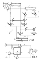
- Binary signals are applied to the filter via two signal leads p and m. These binary signals represent, according to the following Table 1, three transmit signal levels s. Table 1 s pm + 10 0 00 - 01
- the signals on the leads p and m are coupled to the respective two inputs of a NOR-gate 1 and to the two inputs of a logic circuit 3.
- the output signals q and r of gate 1 and logic circuit 3, respectively are linked, as is shown in the respective Tables 2 and 3 following hereinafter, with the signals on the leads p and m.
- the signal q indicates whether the binary signal is representative or not representative of the transmit level zero. If the transmit level is zero, an 1 is entered into the N-bit shift register 2 and, in the opposite case, a 0.
- the signal r indicates whether the binary signal is representative of the transmit level +1 or of the transmit level -1.
- an 1 is entered into the N-bit shift register 4, and a 0 in the opposite case.
- the input signal and the output signals of the shift register 4 control switches 50-5 N , the sliding contact being connected, for a binary signal 1, to a conductor carrying a signal which corresponds to the transmit signal level +1 and for a binary signal 0 to a conductor carrying a signal which corresponds to the transmit signal level -1.
- the fixed contact of the switch 50 carries a voltage having the signal level +1 when the output voltage r of circuit 3 was a 1 and a signal level -1 when the output voltage r of circuit 3 was a 0.
- the signals on the fixed contacts of the switches 50 - 5 N are coupled to the respective inputs of the multiplying circuits 70 - 7 N .
- the input signal and the output signals of the shift register 2 are always coupled via respective inverters 60 - 6 N to the second input terminal of the respective multiplying circuits 70 - 7 N , whilst these signals are also coupled to a first input of respective multipliers 90 - 9 N , whose respective second inputs are connected to a coefficient register, not shown, which can produce coefficient C00 - C ON .
- the output signal of the multipliers 70 - 7 N is coupled to the respective first inputs of multipliers 80 - 8 N whose respective second inputs are coupled to a coefficient register, also not shown, which can produce the coefficients C s0 - C sN .
- the outputs of the multipliers 90 - 9 N are connected to the outputs of the corresponding multipliers 80 - 8 N and these combined output signals are coupled to the inputs 0 - N of a summing circuit 10 whose output produces a linear approximation ê of the echo cancellation signal.
- the coefficient C si therefore does not contribute towards the echo cancellation signal ê.
- multiplier 9 i the signal q(a logic 1) is multiplied by the coefficient C 0i , so that the i th transmit symbol, having a zero level contributes towards the echo cancellation signal which is determined by the zero level coefficient C01, which coefficient also has a relatively low value which in any case is significantly smaller than the transmit signal level amplitude since the zero level to be cancelled is only determined by shifting the zero level between transmission and receiving the transmit signal having the zero level again via the echo path.
- This shift can be produced either by a symmetry in the transmit amplifier, which determines the transmit levels from the signals p and m, or by offset voltages in the hybrid circuit which couples the transmit amplifier to the two-wire connection via which the transmission is effected.
- the coefficient C 0i needs only be capable of assuming a comparatively low value the storage capacity for the register of coefficients C0 can be small and only a very small chip surface area must be reserved for this purpose.
- the coefficient C 0i does not contribute towards the echo cancellation signal as a logic 0 is applied to the first input terminal of multiplier 9 i .
- the output signal of inverter 6 i is a logic 1, so that the input signal of amplifier 7, which in this case is the signal level +1, is multiplied in multiplier 7 i by a logic 1 and thereafter in multiplier 8 i by the coefficient C si , in order to determine the echo cancellation component for the signal i having the level +1.
- the register containing the coefficients C si must have such a storage capacity that the coefficients can assume the full value of the signal level amplitude.
- the signal t i applied to multiplier 7 i is a signal having the -1 level, which signal having the -1 level is multiplied in multiplier 8 i by the coefficient C si .
- Figure 2 shows in what way the adaptive transversal filter according to the invention can be incorporated in a schematically shown transceiver system.
- An input signal is applied via input terminals to the filter 11 and also to a transmit amplifier 12 which converts the signal into transmit symbols s.
- the input signal may consist of the above-described binary signals p and m which are then converted into transmit symbols in accordance with Table 1 by amplifier 12. It is however alternatively possible to apply to the input terminals the signals q and r which already contain the information derived in the circuit of Figure 1 from the input signal by the logic circuits 1 and 3. It will be obvious that amplifier 12 should then convert the signals q and r into transmit symbols in a different manner.
- the system is arranged for communication via a two-wire line, for which purpose a hybrid circuit 13 is provided for a most adequate separation between the received and transmitted signal.
- the system shown in Figure 2 includes a circuit 15 which on the basis of the coefficients used for forming the echo cancellation signal and the signal s ⁇ determines new coefficients and enters them into the coefficient registers in the filter 15. Consequently the circuit 15 constitutes the adaptive control for optimizing the coefficients C 0i and C si in known manner.
- the adaptive control for optimizing the coefficients C 0i and C si has a high convergence rate, that is to say that it results faster in an optimum compensation signal, since the amplitude range of the coefficients C 0i is low the optimum coefficient values are reached fast, as furthermore the register containing the coefficients C si is always addressed when the transmit level is unequal to the zero level, the coefficient values C si are addressed and consequently optimized twice as often as in the case of a filter structure having separate coefficient registers for the +1 level and for the -1 level.
Landscapes
- Engineering & Computer Science (AREA)
- Computer Networks & Wireless Communication (AREA)
- Signal Processing (AREA)
- Power Engineering (AREA)
- Cable Transmission Systems, Equalization Of Radio And Reduction Of Echo (AREA)
- Filters That Use Time-Delay Elements (AREA)
Claims (5)
- Filtre adaptatif transversal comprenant une entrée destinée à recevoir un signal d'entrée discret dans le temps qui est représentatif de trois niveaux de signal; un premier (2) et un second (4) moyen à retard pour produire des versions retardées du signal d'entrée discret dans le temps; un premier et un second registre de coefficients contenant un coefficient spécifique (C₀₀-C0N; CS0-CSN) pour la version non retardée et pour chaque version retardée du signal d'entrée provenant respectivement du premier et du second moyen à retard; un moyen (8₀-8N; 9₀-9N) pour multiplier des coefficients par les versions des signaux d'entrée qui y sont associées et un moyen (10) pour additionner tous les résultats de multiplication obtenus en vue de fournir un signal d'annulation (ê) à une sortie du filtre, caractérisé en ce que le premier moyen à retard (2) contient M versions retardées du signal discret dans le temps, que le premier registre de coefficients contient M+l coefficients (C₀₀-C0N), que le second moyen à retard (4) contient N versions retardées du signal discret dans le temps et que le second registre de coefficients contient N+1 coefficients (CS0-CSN), où M ≦ N, que l'information représentant le niveau central du signal est appliquée au premier moyen à retard (2), que l'information représentant l'un ou l'autre des niveaux extrêmes du signal est appliquée au second moyen à retard (4), et que des moyens sont prévus pour n'appliquer les résultats des multiplications des coefficients (C₀₀-C0N) du premier registre de coefficients par leurs versions associées respectives du signal d'entrée, fournies par le premier moyen à retard (2), au moyen additionneur (10) qu'exclusivement lorsqu'une telle version associée du signal d'entrée contient l'information indiquant la présence du niveau central du signal.
- Filtre transversal suivant la revendication 1, caractérisé en ce que l'information appliquée respectivement au premier (2) et au second (4) moyen à retard est de l'information binaire et que les moyens destinés à n'appliquer au moyen additionneur (10) qu'exclusivement les résultats de multiplication obtenus à l'aide du premier registre de coefficients et du premier moyen à retard (2) sont conçus de manière à toujours bloquer l'application au moyen additionneur (10) d'un résultat de multiplication obtenu à l'aide du second moyen à retard, lorsque la version correspondante du signal d'entrée telle qu'elle est fournie par le premier moyen à retard contient l'information indiquant la présence du niveau central du signal.
- Filtre transversal suivant la revendication 2 dans lequel le premier (2) et le second (4) moyen à retard sont des registres à décalage comprenant des sections comportant chacune M bornes, caractérisé en ce que les moyens destinés à n'appliquer au moyen additionneur (10) qu'exclusivement les résultats de multiplication obtenus à l'aide du premier registre de coefficients et du premier moyen à retard (2) comprennent un inverseur (6₀-6N) et un circuit multiplicateur (7₀-7N) pour chaque paire de bornes correspondantes du premier et du second moyen à retard, l'entrée de l'inverseur étant toujours connectée à une borne du premier moyen à retard, une première entrée du circuit multiplicateur étant toujours connectée à une borne correspondante du second moyen à retard, une seconde entrée du circuit multiplicateur étant connectée à la sortie de l'inverseur et la sortie du circuit multiplicateur étant connectée au moyen pour multiplier le signal provenant du second moyen à retard par son coefficient associé.
- Filtre transversal suivant la revendication 3, caractérisé en ce qu'il comprend N+1 éléments de commutation (S₀-SN), que le signal à une entrée et à chacune des bornes du second moyen à retard forme un signal de commande pour un élément de commutation associé des N+1 éléments de commutation, le signal binaire du second moyen à retard commandant les éléments de commutation d'une manière telle qu'à une première valeur du signal binaire, un niveau positif donné du signal émis et à une seconde valeur du signal binaire, un niveau négatif donné du signal émis soit connecté à la première entrée du circuit multiplicateur (7₀-7N).
- Filtre transversal suivant la revendication 1 ou 2, caractérisé en ce que M = N et que, dans le premier registre de coefficients, les coefficients P jusqu'à et y compris N+1 sont égaux à zéro, où P < N.
Applications Claiming Priority (2)
| Application Number | Priority Date | Filing Date | Title |
|---|---|---|---|
| NL8600816 | 1986-03-28 | ||
| NL8600816A NL8600816A (nl) | 1986-03-28 | 1986-03-28 | Adaptief transversaal filter. |
Publications (2)
| Publication Number | Publication Date |
|---|---|
| EP0241069A1 EP0241069A1 (fr) | 1987-10-14 |
| EP0241069B1 true EP0241069B1 (fr) | 1991-09-11 |
Family
ID=19847796
Family Applications (1)
| Application Number | Title | Priority Date | Filing Date |
|---|---|---|---|
| EP19870200455 Expired EP0241069B1 (fr) | 1986-03-28 | 1987-03-11 | Filtre adaptatif transversal |
Country Status (7)
| Country | Link |
|---|---|
| US (1) | US4786884A (fr) |
| EP (1) | EP0241069B1 (fr) |
| JP (1) | JPH0783240B2 (fr) |
| AU (1) | AU600207B2 (fr) |
| CA (1) | CA1261008A (fr) |
| DE (1) | DE3772810D1 (fr) |
| NL (1) | NL8600816A (fr) |
Families Citing this family (3)
| Publication number | Priority date | Publication date | Assignee | Title |
|---|---|---|---|---|
| NL8600816A (nl) | 1986-03-28 | 1987-10-16 | At & T & Philips Telecomm | Adaptief transversaal filter. |
| US5303228A (en) * | 1991-08-27 | 1994-04-12 | Industrial Technology Research Institute | A far-end echo canceller with a digital filter for simulating a far end echo containing a frequency offset |
| US5339264A (en) * | 1992-07-27 | 1994-08-16 | Tektronix, Inc. | Symmetric transposed FIR digital filter |
Family Cites Families (7)
| Publication number | Priority date | Publication date | Assignee | Title |
|---|---|---|---|---|
| GB1108415A (en) * | 1966-05-06 | 1968-04-03 | Int Standard Electric Corp | Echo suppression in long distance telephone circuits |
| DE2060159C3 (de) * | 1970-12-07 | 1978-06-15 | Siemens Ag, 1000 Berlin Und 8000 Muenchen | Adaptives Filter |
| DE3037778A1 (de) * | 1980-10-07 | 1982-05-19 | Robert Bosch Gmbh, 7000 Stuttgart | Verfahren zur zeitlichen korrektur von digitalen schaltsignalen |
| NL8006543A (nl) * | 1980-12-02 | 1982-07-01 | Philips Nv | Zelfinstellend filter. |
| JPS587935A (ja) * | 1981-07-07 | 1983-01-17 | Kokusai Denshin Denwa Co Ltd <Kdd> | トランスバーサル形スミアデスミアフイルタ |
| US4707824A (en) * | 1983-12-15 | 1987-11-17 | Nec Corporation | Method and apparatus for cancelling echo |
| NL8600816A (nl) | 1986-03-28 | 1987-10-16 | At & T & Philips Telecomm | Adaptief transversaal filter. |
-
1986
- 1986-03-28 NL NL8600816A patent/NL8600816A/nl not_active Application Discontinuation
-
1987
- 1987-03-11 EP EP19870200455 patent/EP0241069B1/fr not_active Expired
- 1987-03-11 DE DE8787200455T patent/DE3772810D1/de not_active Expired - Lifetime
- 1987-03-20 US US07/028,631 patent/US4786884A/en not_active Expired - Lifetime
- 1987-03-26 CA CA000533102A patent/CA1261008A/fr not_active Expired
- 1987-03-27 JP JP62071908A patent/JPH0783240B2/ja not_active Expired - Fee Related
- 1987-03-30 AU AU70725/87A patent/AU600207B2/en not_active Ceased
Also Published As
| Publication number | Publication date |
|---|---|
| CA1261008A (fr) | 1989-09-26 |
| EP0241069A1 (fr) | 1987-10-14 |
| NL8600816A (nl) | 1987-10-16 |
| JPH0783240B2 (ja) | 1995-09-06 |
| US4786884A (en) | 1988-11-22 |
| AU7072587A (en) | 1987-10-01 |
| AU600207B2 (en) | 1990-08-02 |
| DE3772810D1 (de) | 1991-10-17 |
| JPS62294314A (ja) | 1987-12-21 |
Similar Documents
| Publication | Publication Date | Title |
|---|---|---|
| US4605826A (en) | Echo canceler with cascaded filter structure | |
| US4621172A (en) | Fast convergence method and system for echo canceller | |
| EP0541225B1 (fr) | Egaliseur pour un appareil de réception de données | |
| AU609715B2 (en) | Adaptive filter for producing an echo cancellation signal in a transceiver system for duplex digital communication through one single pair of conductors | |
| EP0145022B1 (fr) | Procédé et dispositif pour la compensation d'écho | |
| US5375147A (en) | Jitter compensating device | |
| EP0543568A2 (fr) | Filtrage à haute résolution utilisant des processeurs à basse résolution | |
| US4920530A (en) | Adaptive time-discrete filter for forming a cancelling signal from synchronous data symbols | |
| US4272648A (en) | Gain control apparatus for digital telephone line circuits | |
| EP0241069B1 (fr) | Filtre adaptatif transversal | |
| JPH0230226A (ja) | エコーキャンセラ | |
| US6263015B1 (en) | Analog/digital integrated subscriber circuit | |
| EP0246425B1 (fr) | Dispositif d'annulation d'échos dans un système de transmission numérique en duplex | |
| JP2591230B2 (ja) | データ復号装置 | |
| JP2511157B2 (ja) | 自動等化器 | |
| JPH0473649B2 (fr) | ||
| EP0875992A2 (fr) | Filtre numérique à réponse impulsionnelle longue | |
| JPS58223928A (ja) | エコ−キヤンセラ−装置 | |
| JPS59194537A (ja) | 自動等化器 | |
| JPH07226704A (ja) | 適応等化器 | |
| JPH07123237B2 (ja) | デ−タ伝送用エコ−キヤンセル装置 | |
| JPH01180126A (ja) | エコーキャンセラ | |
| JPH0473331B2 (fr) | ||
| JPH03284010A (ja) | 適応型通信路インパルスレスポンス推定方式 | |
| JPS61206330A (ja) | エコ−キヤンセラ |
Legal Events
| Date | Code | Title | Description |
|---|---|---|---|
| PUAI | Public reference made under article 153(3) epc to a published international application that has entered the european phase |
Free format text: ORIGINAL CODE: 0009012 |
|
| AK | Designated contracting states |
Kind code of ref document: A1 Designated state(s): BE DE FR GB IT NL SE |
|
| 17P | Request for examination filed |
Effective date: 19880402 |
|
| 17Q | First examination report despatched |
Effective date: 19900202 |
|
| RAP1 | Party data changed (applicant data changed or rights of an application transferred) |
Owner name: AT&T NETWORK SYSTEMS INTERNATIONAL B.V. Owner name: APT NEDERLAND B.V. |
|
| GRAA | (expected) grant |
Free format text: ORIGINAL CODE: 0009210 |
|
| AK | Designated contracting states |
Kind code of ref document: B1 Designated state(s): BE DE FR GB IT NL SE |
|
| REF | Corresponds to: |
Ref document number: 3772810 Country of ref document: DE Date of ref document: 19911017 |
|
| ET | Fr: translation filed | ||
| ITF | It: translation for a ep patent filed | ||
| RAP4 | Party data changed (patent owner data changed or rights of a patent transferred) |
Owner name: AT&T NETWORK SYSTEMS INTERNATIONAL B.V. Owner name: AT&T NETWORK SYSTEMS NEDERLAND B.V. |
|
| NLT1 | Nl: modifications of names registered in virtue of documents presented to the patent office pursuant to art. 16 a, paragraph 1 |
Owner name: AT&T NETWORK SYSTEMS NEDERLAND B.V. TE HILVERSUM. |
|
| PLBE | No opposition filed within time limit |
Free format text: ORIGINAL CODE: 0009261 |
|
| STAA | Information on the status of an ep patent application or granted ep patent |
Free format text: STATUS: NO OPPOSITION FILED WITHIN TIME LIMIT |
|
| 26N | No opposition filed | ||
| EAL | Se: european patent in force in sweden |
Ref document number: 87200455.1 |
|
| PGFP | Annual fee paid to national office [announced via postgrant information from national office to epo] |
Ref country code: BE Payment date: 20000106 Year of fee payment: 14 |
|
| PGFP | Annual fee paid to national office [announced via postgrant information from national office to epo] |
Ref country code: SE Payment date: 20001227 Year of fee payment: 15 |
|
| PGFP | Annual fee paid to national office [announced via postgrant information from national office to epo] |
Ref country code: FR Payment date: 20010222 Year of fee payment: 15 |
|
| PGFP | Annual fee paid to national office [announced via postgrant information from national office to epo] |
Ref country code: GB Payment date: 20010226 Year of fee payment: 15 |
|
| PGFP | Annual fee paid to national office [announced via postgrant information from national office to epo] |
Ref country code: NL Payment date: 20010312 Year of fee payment: 15 |
|
| PG25 | Lapsed in a contracting state [announced via postgrant information from national office to epo] |
Ref country code: BE Free format text: LAPSE BECAUSE OF NON-PAYMENT OF DUE FEES Effective date: 20010331 |
|
| BERE | Be: lapsed |
Owner name: AT&T NETWORK SYSTEMS INTERNATIONAL B.V. Effective date: 20010331 |
|
| REG | Reference to a national code |
Ref country code: GB Ref legal event code: IF02 |
|
| PG25 | Lapsed in a contracting state [announced via postgrant information from national office to epo] |
Ref country code: GB Free format text: LAPSE BECAUSE OF NON-PAYMENT OF DUE FEES Effective date: 20020311 |
|
| PG25 | Lapsed in a contracting state [announced via postgrant information from national office to epo] |
Ref country code: SE Free format text: LAPSE BECAUSE OF NON-PAYMENT OF DUE FEES Effective date: 20020312 |
|
| PG25 | Lapsed in a contracting state [announced via postgrant information from national office to epo] |
Ref country code: NL Free format text: LAPSE BECAUSE OF NON-PAYMENT OF DUE FEES Effective date: 20021001 |
|
| EUG | Se: european patent has lapsed |
Ref document number: 87200455.1 |
|
| GBPC | Gb: european patent ceased through non-payment of renewal fee |
Effective date: 20020311 |
|
| PG25 | Lapsed in a contracting state [announced via postgrant information from national office to epo] |
Ref country code: FR Free format text: LAPSE BECAUSE OF NON-PAYMENT OF DUE FEES Effective date: 20021129 |
|
| NLV4 | Nl: lapsed or anulled due to non-payment of the annual fee |
Effective date: 20021001 |
|
| REG | Reference to a national code |
Ref country code: FR Ref legal event code: ST |
|
| PGFP | Annual fee paid to national office [announced via postgrant information from national office to epo] |
Ref country code: DE Payment date: 20060314 Year of fee payment: 20 |
|
| PGFP | Annual fee paid to national office [announced via postgrant information from national office to epo] |
Ref country code: IT Payment date: 20060331 Year of fee payment: 20 |