EP0239128A2 - Dispositif de traitement de données avec fonction d'accès de mémoire directe - Google Patents
Dispositif de traitement de données avec fonction d'accès de mémoire directe Download PDFInfo
- Publication number
- EP0239128A2 EP0239128A2 EP87104610A EP87104610A EP0239128A2 EP 0239128 A2 EP0239128 A2 EP 0239128A2 EP 87104610 A EP87104610 A EP 87104610A EP 87104610 A EP87104610 A EP 87104610A EP 0239128 A2 EP0239128 A2 EP 0239128A2
- Authority
- EP
- European Patent Office
- Prior art keywords
- interrupt
- data
- direct memory
- address
- memory
- Prior art date
- Legal status (The legal status is an assumption and is not a legal conclusion. Google has not performed a legal analysis and makes no representation as to the accuracy of the status listed.)
- Withdrawn
Links
Images
Classifications
-
- G—PHYSICS
- G06—COMPUTING; CALCULATING OR COUNTING
- G06F—ELECTRIC DIGITAL DATA PROCESSING
- G06F13/00—Interconnection of, or transfer of information or other signals between, memories, input/output devices or central processing units
- G06F13/14—Handling requests for interconnection or transfer
- G06F13/20—Handling requests for interconnection or transfer for access to input/output bus
- G06F13/32—Handling requests for interconnection or transfer for access to input/output bus using combination of interrupt and burst mode transfer
Definitions
- This invention relates to a data processing device which is fabricated on a single semiconductor chip and which can have a direct access to a memory.
- DMA direct memory-access
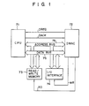
- Fg. I shows a block diagram of a conventional computer system with the DMA function, for example, a micro computer system.
- the system comprises central processing unit (CPU) 71 and direct memory-access controller (DMAC) 72.
- the system further comprises a read/write memory 73, 1/0 interface 74, data bus 75, and address bus 76.
- DMAC 72 renders a DMA- request signal DREQ active to transfer data from memory 73 to 1/O interface 74 by using the DMA function.
- DREQ DMA- request signal
- CPU 7l renders DMA acknowledge signal DACK active.
- the bus- use right is transferred to DMAC 72.
- DMAC 72 addresses memory 73 and 1/0 interface 74.
- Read control signal RD is made active for memory 73.
- Write control signal WR is made active for 1/0 interface 74.
- data is read out from memory 73 and written into I/O interface 74.
- the DMA data transfer is executed between memory 73 and VO interface 74.
- DMA data transfer does not need the fetching of instructions by CPU 7i or the decoding of instructions.
- the DMA data transfer system can transfer data at speed several times higher than in the normal program processing achieved by CPU 71.
- Such an operation needs the special hardware of DMAC 72, as has been just mentioned.
- DMAC 72 needs many functional components: a source address register for storing an address of the data to transfer, a destination address register for storing an address to which the data will be transferred to, a transfer counter register for storing the number of data transfers, an incrementor for incrementing the contents of the source address register and the destination address register, a decrementor for decrementing the contents of the source address register and the destination address register, and an interface with the CPU, for example. Therefore, if the DMAC is formed in a single chip, the hardware for the microcomputer extremely increases, inevitably increasing the chip size and the manufacture cost
- an object of this invention is to provide a data processing device which can have a direct access to a memory and can realize the high speed DMA data transfer with a relatively small hardware increase.
- a data processing device comprising: interrupt detect means for detecting an interrupt signal and for generating a vector corresponding to the interrupt signal detected; control signal generating means for generating, in response to vector, a control signal showing whether or not the interrupt is a normal interrupt or an interrupt for requesting the direct memory-access operation; logical operation processing means for storing the control function as a micro-codes to achieve the direct memory access operation, and for sequentially reading out the micro-codes when the control signal generating means generates a control signal corresponding to the interrupt signal requesting the direct memory-access operation, whereby the logical operation processing means executes and controls the direct memory-access operation; and parameter memory means for storing parameters necessary for the direct memory-access operation, and for reading out these parameters in response to the vector to supply them to the logical operation processing means.
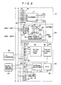
- Fig. 2 shows a block diagram illustrating a data processing device according to this invention.
- the device comprises 8-bit data buses DBO to DB7 and 16-bit address buses ABO to ABI5.
- the device further comprises interrupt controller 10, DMA controller 20, and CPU 30. These components are all integrated into a single chip.
- Data buses DBO to DB7 and address buses ABO to ABI5 are connected to 1/0 interface 50 and read/write memory 60.
- Interrupt controller 10 contains encoder II coupled with 16 interrupt signal lines IRO to IRIS. Interrupt states of these sixteen signal lines IRO to IR15 are encoded into a vector made up of binary signals A to D of 4 bits. When an interrupt is present in any one of signal lines IRO to IRI5, interrupt request signal INTREQ is generated by encoder II and applied to CPU 30.
- Interrupt controller 10 contains vector converter 12 which is for converting the 4-bit vector made of signals A to D output from encoder II into an 8-bit vector.
- Vector converter 12 is made up of eight transfer gates 13. Of the eight transfer gates 13, those of the lower three bits are supplied with the earth potential corresponding to "0" of data. Those of the 4th bits to the 7th bits are supplied with binary signals A to D. The earth potential corresponding to the data "0" is supplied to the 8th bit as the most significant bit (MSB).
- vector read signal VRD (described later), transfer gates 13 produce the data as input thereto, to convert the 4-bit data into 8-bit data.
- the converted 8-bit vector (hereinafter referred to as "V", and expressed in hexadecimal number) is output to data buses DBO to DB7.
- DMA controller 20 is provided with vector latch circuit 21 for latching binary signal A to D of 4 bits output from encoder II, which are contained in the vector "V" output onto data buses DBO to DB7.
- Vector latch circuit 21 latches this vector in response to vector read signal VRD.
- the vector made up of signals A to D is supplied to decoder 22.
- Decoder 22 converts the vector consisting of four bits binary signals A to D into 16 signals 0 to 15. These sixteen signals are applied to first input terminals of 16 AND gates 23, which are provided in DMA controller 20.
- DMA controller 20 further contains DMA enable flag register 24 for latching 16-bit data.
- the 16-bit data to be latched in DMA enable flag register 24 is preset corresponding to the interrupt by 16 interrupt signal lines IRO to IRIS.
- CPU30 comprises mode register (MR) 31, counter 32, instruction register (IR) 33, micro-code ROM 34, timing signal generator 35, arithmetic/logic unit 36, program counter PC (not shown), intemal register 37, address latch 38, data latch 39, and latches 40 and 41.
- Micro-code ROM 34 stores micro-codes. This ROM 34 is addressed by the outputs of mode register 31, counter 32 and instruction register 33, and produces the micro-code from the addressed memory location. The micro-code as read out from micro-code ROM 34 is supplied to timing signal generator 35. In response- to the supplied micro-code, timing signal generator 35 generates various types of timing signals for controlling the operation of the whole device.
- Arithmetic/logic unit (ALU) 36 executes arithmetic and logical operations.
- Internal register 37 is made up of various counters and registers such as program status word PSW (not shown).
- Address latch 38 is composed of upper address latch ALH for latching the addresses of upper 8 bits on address bus ABO to ABI5, and lower address latch ALL for latching the addresses of lower 8 bits.
- Data latch 39 latches the data on data buses DBO to DB7.
- Latch 40 latches the data of hexadecimal "00”.
- Latch 41 latches the data of hexadecimal "FF”.
- Mode register 31 is supplied with interrupt request signal INTREQ which is generated by interrupt controller 10, and control signal DMA/ I NT which is generated by DMA controller 20. These signals are both stored in mode register 31.
- Micro-code ROM 34 stores the programs as micro-codes for controlling the operation of the whole device. This program include the microprogram for executing and controlling the normal processing and the normal interrupt processing, and also the microprogram for executing and controlling the DMA operation.
- Timing signal generator 35 generates, in response to the micro-code read out from micro-code ROM 34, various types of timing signals including vector read signal VRD.
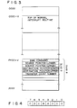
- Fig. 3 shows a data memory map of a data area to which the data processing device is accessible.
- the data area contains I/O interface 50 and memory 60. This data area is sized such that it is defined by the addresses of hexadecimal "0000" to "FFFF". The area having address "0000" + “V” as the top address is included in memory 60. In this area, the processing program for normal interrupt routine is stored. The area starting at address "FFOO" + "V” is included in memory 60.
- the DMA command is stored in the Ist byte of the 8-byte area starting at address ''FF00" + “V”. This command contains many parameters. The first parameter designates if the DMA transfer is the I]-byte transfer or the 2-byte transfer.
- the second param-- eter indicates if the contents of the source pointer indicating the data area of the data transfer source is incremented or decremented every data transfer, or left unchanged.
- the third parameter indicates if the content of the destination pointer indicating the data area of the data transfer destination is incremented or decremented every data transfer, or left unchanged.
- the second byte location stores the lower order bits of the source pointer.
- the third byte location stores the upper order bits of the source pointer.
- the fourth byte location stores the lower order bits of the destination pointer.
- the fifth byte location stores the upper order bits of the destination pointer.
- the sixth byte location stores the transfer count number equal to the maximum number of data transfers. No data is stored in the seventh and eighth bytes for the reason that the address designated by vector "V" is changed every 8 bytes.
- each transfer gate 13 of vector converter 12 in interrupt controller 10 operates, vector "V" is output onto data buses DBO to DB7.
- the Oth to second bits, and the seventh bit are fixed to "0".
- the third bit to sixth bit are used as output data A to D and output from encoder II.
- the third bit of the vector "V” is set to "I”. This is "08" of hexadecimal number.
- Vector "V” is input to DMA controller 20 via data buses DBO to DB7.
- the data from the third bit to the sixth bit of vector "V" i.e. signal A to D, are latched in vector latch circuit 21.
- the latched data is converted by decoder 22 to make only one of the sixteen output signals active.
- the interrupt signal line IRI is used as an interrupt signal line for requesting the DMA operation
- the flag data of the DMA enable flag register 24, which corresponds to signal line IRI is set to "I”.
- the output signal of AND gate 23 to which the signal made active by decoder 22 is supplied is "I”.
- the output signal DMA/ INT of OR gate 25 is made active.
- micro-code ROM 34 When signal DMA/ I NT is made active, micro-code ROM 34 is addressed by the output signal from mode register 31 in CPU 30. The micro-code is read out from the memory area as addressed. This micro-code is the top of the micro-code for executing and controfling the DMA operation.
- the vector “V” output from interrupt controller 10 is also input to CPU 30, by way of data buses DBO to DB7.
- This vector “V” is temporarily stored in internal register 37 in response to the timing signal from timing signal generator 35.
- the vector “V” as stored in internal register 37 is then transferred to lower order address latch ALL of address latch circuit 38. Then, it is latched by this latch.
- the data "FF” latched by latch circuit 41 is transferred to upper order address latch ALH of address latch circuit 38. Then, it is latched by this latch.
- address "FF00" + “V” is latched in address latch circuit 38. Then, this address is output to address buses ABO to AB15.
- This address signal sequentially reads out the data and address value, i.e.
- DMA command, source pointer, destination pointer, and transfer count number which are necessary for the DMA operation as prestored with 6 bytes length in the memory area of memory 60.
- the memory area is contained in the data area and has "FFOO" + "V" at the top address.
- the data and address value contain DMA command, source pointer, destination pointer, and the transfer count number.
- Fig. 3 The read out data are sent to internal register 37 in CPU 30.
- the DMA operation which is based on the read out data and address value, is executed under control of the micro-codes as prestored in micro-code ROM 34 in CPU 30.
- the addressing of micro-code ROM 34 is performed at this time by the output signal from counter 32.
- CPU 30 updates the data and address value for the DMA operation, such as source pointer or destination pointer, and transfer count number. Those updated ones are stored in the original data area of memory 60, again. The operation similar to the above is performed again. Such an operation is repeated several times. With progression of the operation, it is detected that the transfer count number stored at the 6th " byte in the data area starting at address "FFOO" + "V" is zero. At this time, CPU 30 decides that the DMA transfer is completed, and stops the DMA transfer operation.
- one of interrupt signal lines IRI to IRI5 is rendered active, and the interrupt signal requests the normal interrupt.
- the data latched in DMA enable flag register 24 corresponding to this interrupt has been set to "0".
- the output signal from AND gate 23, which has been supplied with the signal made active by decoder 22, is "0".
- the output signal DMA/ I NT of OR gate 25 is made nonactive.
- the micro-code as read out from micro-code ROM 34 is located at the top of the program for executing the normal interrupt.
- the vector "V" from internal register 37 is sent to lower order address latch ALL of address latch circuit 38.
- the data "00" latched in latch circuit 40 is sent to the upper order address latch ALH of address latch circuit 38, and latched therein. In this way, address "0000" + “V” is latched in address latch circuit 38. This address is then output onto address buses ABO to ABI5. By this address signal, the normal interrupt routine is read out from the memory area of memory 60 starting at address "0000" + "V", which is contained in the data area of Fig. 3. The interrupt routine as read out is executed in the conventional way.
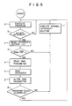
- step "a” A predetermined program prestored in memory 60 is executed (step “a").
- step "b" Check is made as to whether or not the data processing device accepts the interrupt from the peripheral device (step “b”). The detection of the interrupt accept is performed depending on whether or not the interrupt request signal INTREQ is generated in interrupt controller 10. If the interrupt is rejected, control goes back to step “a” where execution of the program is continued.
- step "c” vector "V” is read out (step “c”). Following the read out of vector "V”, it is checked whether or not the control signal DMA/ I NT as generated by DMA controller 20 is "I” or not (step “d”). If the answer is "I” and the interrupt is the one for requesting the DMA transfer, the DMA parameter is read out from the memory area at "FF00" + “V” in the data area (step “e”).
- the DMA transfer is executed by using the parameter (step "f").
- the details of the DMA transfer follows.
- the contents in the memory address location as indicated by source pointer within the 6- byte length starting at address "FF00" + “V” in Fig. 3 are transferred to internal register 37 in CPU 30, and temporarily stored therein. This is a read- cycle.
- the data stored in internal register 37 is transferred to the location at the address as indicated by the destination pointer with the 6-byte length, and stored in this memory. location. This is a write-cycle. In the 2-byte transfer, such an operation is repeated two times.
- step "g" the transfer counter number in the DMA parameter is "0" (step "h"). In this step, if the transfer counter number is not 0, control returns to step "a" since the DMA transfer is not yet completed.
- step “d” When in step “d” it is detected that signal DMA/ I NT is "0" and the interrupt is for requesting the normal interrupt, the program counter (PC) and the program status word (PSW) are pushed. A program is read out from the memory location at address "0000" + “V” in the data area, so that the normal interrupt is processed (step " I ").
- step "h” detects that the transfer counter number is "0"
- CPU decides that the DMA transfer has been ended and executes stop "i”.
- the end of the DMA transfer can be detected by CPU 30.
- the normal interrupt is processed, so that the processing is executed using the data as obtained through the DMA transfer.
- the data processing device is realized by additional applying DMA controller 20 to the conventional data processing device with the data interrupt function.
- the function of the prior DMAC is realised by using the micro-codes in micro-code ROM 34 and the stored data in the data area.
- the hardware used for the whole data processing device can remarkably be reduced when compared with the prior device using the DMAC dedicated for the DMA transfer.
- the data processing device of this invention needs the hardware increased by an amount necessary for storing the data for the DMA interrupt processing by DMA controller 20 and micro-code ROM 34. This increase of hardware is much smaller than that due to use of the dedicated DMAC.
- the DMA transfer speed is controlled by the micro-codes read out from micro-code ROM 34. Therefore, it is slightly slower than that when the dedicated DMAC is used, but can be remarkably improved when compared with that in the case of the interrupt processing by the program processing.
Applications Claiming Priority (2)
| Application Number | Priority Date | Filing Date | Title |
|---|---|---|---|
| JP69215/86 | 1986-03-27 | ||
| JP61069215A JPS62226257A (ja) | 1986-03-27 | 1986-03-27 | 演算処理装置 |
Publications (2)
| Publication Number | Publication Date |
|---|---|
| EP0239128A2 true EP0239128A2 (fr) | 1987-09-30 |
| EP0239128A3 EP0239128A3 (fr) | 1990-01-17 |
Family
ID=13396272
Family Applications (1)
| Application Number | Title | Priority Date | Filing Date |
|---|---|---|---|
| EP87104610A Withdrawn EP0239128A3 (fr) | 1986-03-27 | 1987-03-27 | Dispositif de traitement de données avec fonction d'accès de mémoire directe |
Country Status (3)
| Country | Link |
|---|---|
| US (1) | US5063498A (fr) |
| EP (1) | EP0239128A3 (fr) |
| JP (1) | JPS62226257A (fr) |
Cited By (1)
| Publication number | Priority date | Publication date | Assignee | Title |
|---|---|---|---|---|
| EP0426081A2 (fr) * | 1989-10-30 | 1991-05-08 | Kabushiki Kaisha Toshiba | Dispositif de commande programmable avec unité de commande d'interruption pour déterminer la priorité de demandes d'interruption de plusieurs unités d'entrée/de sortie et pour la génération de vecteur d'interruption |
Families Citing this family (16)
| Publication number | Priority date | Publication date | Assignee | Title |
|---|---|---|---|---|
| JPH01258163A (ja) * | 1988-04-08 | 1989-10-16 | Fujitsu Ltd | ダイレクトメモリアクセス制御装置 |
| JPH02199542A (ja) * | 1989-01-30 | 1990-08-07 | Ricoh Co Ltd | 情報処理装置 |
| JP2539058B2 (ja) * | 1989-03-30 | 1996-10-02 | 三菱電機株式会社 | デ―タプロセッサ |
| GB2271204B (en) * | 1992-10-01 | 1996-01-03 | Digital Equipment Int | Digital system memory access |
| DE19733527A1 (de) * | 1997-08-02 | 1999-02-04 | Philips Patentverwaltung | Kommunikationssystem mit einer DMA-Einheit |
| DE19733526A1 (de) * | 1997-08-02 | 1999-02-04 | Philips Patentverwaltung | Kommunikationssystem mit einer Schnittstelle |
| EP1116352A4 (fr) * | 1998-09-24 | 2003-09-17 | Xircom Wireless Inc | Gestion d'operations en creneaux pour communication sans fil |
| US6260082B1 (en) * | 1998-12-23 | 2001-07-10 | Bops, Inc. | Methods and apparatus for providing data transfer control |
| US6810443B2 (en) | 2002-12-31 | 2004-10-26 | Intel Corporation | Optical storage transfer performance |
| US7243178B2 (en) * | 2003-05-16 | 2007-07-10 | Intel Corporation | Enable/disable claiming of a DMA request interrupt |
| US7895411B2 (en) * | 2003-10-02 | 2011-02-22 | Nvidia Corporation | Physics processing unit |
| US7739479B2 (en) * | 2003-10-02 | 2010-06-15 | Nvidia Corporation | Method for providing physics simulation data |
| US20050086040A1 (en) * | 2003-10-02 | 2005-04-21 | Curtis Davis | System incorporating physics processing unit |
| US20050251644A1 (en) * | 2004-05-06 | 2005-11-10 | Monier Maher | Physics processing unit instruction set architecture |
| US8386704B2 (en) * | 2006-10-25 | 2013-02-26 | HGST Netherlands B.V. | Techniques for improving hard disk drive efficiency |
| JP7249968B2 (ja) * | 2020-03-09 | 2023-03-31 | 株式会社東芝 | 情報処理装置およびストレージ |
Citations (1)
| Publication number | Priority date | Publication date | Assignee | Title |
|---|---|---|---|---|
| EP0169577A2 (fr) * | 1984-07-27 | 1986-01-29 | Hitachi, Ltd. | Micro-ordinateur |
Family Cites Families (7)
| Publication number | Priority date | Publication date | Assignee | Title |
|---|---|---|---|---|
| JPS5248440A (en) * | 1975-10-15 | 1977-04-18 | Toshiba Corp | Memory access control system |
| US4090238A (en) * | 1976-10-04 | 1978-05-16 | Rca Corporation | Priority vectored interrupt using direct memory access |
| US4133030A (en) * | 1977-01-19 | 1979-01-02 | Honeywell Information Systems Inc. | Control system providing for the transfer of data in a communications processing system employing channel dedicated control blocks |
| US4532587A (en) * | 1981-08-26 | 1985-07-30 | Texas Instruments Incorporated | Single chip processor connected to an external memory chip |
| JPS6019269A (ja) * | 1983-07-13 | 1985-01-31 | Nec Corp | 高速デ−タ転送方式 |
| US4648029A (en) * | 1984-08-27 | 1987-03-03 | International Business Machines Corporation | Multiplexed interrupt/DMA request arbitration apparatus and method |
| US4716523A (en) * | 1985-06-14 | 1987-12-29 | International Business Machines Corporation | Multiple port integrated DMA and interrupt controller and arbitrator |
-
1986
- 1986-03-27 JP JP61069215A patent/JPS62226257A/ja active Granted
-
1987
- 1987-03-27 EP EP87104610A patent/EP0239128A3/fr not_active Withdrawn
-
1989
- 1989-07-20 US US07/383,266 patent/US5063498A/en not_active Expired - Lifetime
Patent Citations (1)
| Publication number | Priority date | Publication date | Assignee | Title |
|---|---|---|---|---|
| EP0169577A2 (fr) * | 1984-07-27 | 1986-01-29 | Hitachi, Ltd. | Micro-ordinateur |
Non-Patent Citations (1)
| Title |
|---|
| 18th NUCLEAR SCIENCE SYMPOSIUM AND 3rd NUCLEAR POWER SYSTEMS SYMPOSIUM, San Francisco, 3rd-5th November 1971, pages 682-688, New York, US; J.A. BUCHANAN et al.: "Camac multi-microprogrammed IO processor" * |
Cited By (3)
| Publication number | Priority date | Publication date | Assignee | Title |
|---|---|---|---|---|
| EP0426081A2 (fr) * | 1989-10-30 | 1991-05-08 | Kabushiki Kaisha Toshiba | Dispositif de commande programmable avec unité de commande d'interruption pour déterminer la priorité de demandes d'interruption de plusieurs unités d'entrée/de sortie et pour la génération de vecteur d'interruption |
| EP0426081A3 (en) * | 1989-10-30 | 1991-12-18 | Kabushiki Kaisha Toshiba | Programmable controller having interrupt controller for determining priority for interrupt requests from a plurality of i/o devices and generating interrupt vector |
| US5430879A (en) * | 1989-10-30 | 1995-07-04 | Kabushiki Kaisha Toshiba | Programmable controller having a means to accept a plurality of I/O devices mountable in arbitrary slots |
Also Published As
| Publication number | Publication date |
|---|---|
| JPS62226257A (ja) | 1987-10-05 |
| US5063498A (en) | 1991-11-05 |
| EP0239128A3 (fr) | 1990-01-17 |
| JPH0442699B2 (fr) | 1992-07-14 |
Similar Documents
| Publication | Publication Date | Title |
|---|---|---|
| EP0239128A2 (fr) | Dispositif de traitement de données avec fonction d'accès de mémoire directe | |
| US4090238A (en) | Priority vectored interrupt using direct memory access | |
| US5212795A (en) | Programmable DMA controller | |
| US4144562A (en) | System and method for increasing microprocessor output data rate | |
| US4038642A (en) | Input/output interface logic for concurrent operations | |
| US4349873A (en) | Microprocessor interrupt processing | |
| US3962682A (en) | Split low order internal address bus for microprocessor | |
| EP0458304B1 (fr) | Appareil de commande de transfert pour l'accès direct en mémoire et utilisation | |
| US4010448A (en) | Interrupt circuitry for microprocessor chip | |
| JP3982716B2 (ja) | 梯子図マクロ命令を使用したプログラマブルコントローラ | |
| US4053950A (en) | Residual status reporting during chained cycle steal input/output operations | |
| US4268908A (en) | Modular macroprocessing system comprising a microprocessor and an extendable number of programmed logic arrays | |
| JP3676882B2 (ja) | マイクロプロセッサ及びその周辺装置 | |
| US5432943A (en) | Data processing apparatus having interruption control unit | |
| US5287471A (en) | Data transfer controller using direct memory access method | |
| US4016546A (en) | Bus switch coupling for series-coupled address bus sections in a microprocessor | |
| US4037204A (en) | Microprocessor interrupt logic | |
| US5724604A (en) | Data processing system for accessing an external device and method therefor | |
| KR900004291B1 (ko) | 데이터 프로세서 | |
| US4004281A (en) | Microprocessor chip register bus structure | |
| US4030079A (en) | Processor including incrementor and program register structure | |
| US4040035A (en) | Microprocessor having index register coupled to serial-coupled address bus sections and to data bus | |
| US4032896A (en) | Microprocessor having index register coupled to serial-coupled address bus sections and to data bus | |
| US4153942A (en) | Industrial control processor | |
| CA1203917A (fr) | Systeme a micro-ordinateurs |
Legal Events
| Date | Code | Title | Description |
|---|---|---|---|
| PUAI | Public reference made under article 153(3) epc to a published international application that has entered the european phase |
Free format text: ORIGINAL CODE: 0009012 |
|
| 17P | Request for examination filed |
Effective date: 19870424 |
|
| AK | Designated contracting states |
Kind code of ref document: A2 Designated state(s): DE FR GB |
|
| PUAL | Search report despatched |
Free format text: ORIGINAL CODE: 0009013 |
|
| AK | Designated contracting states |
Kind code of ref document: A3 Designated state(s): DE FR GB |
|
| 17Q | First examination report despatched |
Effective date: 19911205 |
|
| STAA | Information on the status of an ep patent application or granted ep patent |
Free format text: STATUS: THE APPLICATION IS DEEMED TO BE WITHDRAWN |
|
| 18D | Application deemed to be withdrawn |
Effective date: 19930217 |
|
| RIN1 | Information on inventor provided before grant (corrected) |
Inventor name: ABE, AKIHITOC/O PATENT DIVISION Inventor name: HIRAHARA, ZIROC/O PATENT DIVISION |