EP0239085B1 - Device for micro-movement of objects - Google Patents
Device for micro-movement of objects Download PDFInfo
- Publication number
- EP0239085B1 EP0239085B1 EP87104373A EP87104373A EP0239085B1 EP 0239085 B1 EP0239085 B1 EP 0239085B1 EP 87104373 A EP87104373 A EP 87104373A EP 87104373 A EP87104373 A EP 87104373A EP 0239085 B1 EP0239085 B1 EP 0239085B1
- Authority
- EP
- European Patent Office
- Prior art keywords
- movement
- elements
- scanning
- movement device
- movement elements
- Prior art date
- Legal status (The legal status is an assumption and is not a legal conclusion. Google has not performed a legal analysis and makes no representation as to the accuracy of the status listed.)
- Expired - Lifetime
Links
- 238000010276 construction Methods 0.000 claims description 5
- 238000009413 insulation Methods 0.000 claims description 4
- 238000003754 machining Methods 0.000 claims 1
- 239000000463 material Substances 0.000 abstract description 9
- 238000000034 method Methods 0.000 description 5
- 239000012799 electrically-conductive coating Substances 0.000 description 3
- 230000005484 gravity Effects 0.000 description 3
- 238000004519 manufacturing process Methods 0.000 description 3
- 241000894006 Bacteria Species 0.000 description 1
- 241001000287 Helvetia Species 0.000 description 1
- 241000700605 Viruses Species 0.000 description 1
- 230000003321 amplification Effects 0.000 description 1
- 238000005452 bending Methods 0.000 description 1
- 230000015572 biosynthetic process Effects 0.000 description 1
- 229910010293 ceramic material Inorganic materials 0.000 description 1
- 238000006243 chemical reaction Methods 0.000 description 1
- 239000011248 coating agent Substances 0.000 description 1
- 238000000576 coating method Methods 0.000 description 1
- 238000005336 cracking Methods 0.000 description 1
- 229910003460 diamond Inorganic materials 0.000 description 1
- 239000010432 diamond Substances 0.000 description 1
- 238000006073 displacement reaction Methods 0.000 description 1
- 230000005684 electric field Effects 0.000 description 1
- 238000005516 engineering process Methods 0.000 description 1
- 238000010353 genetic engineering Methods 0.000 description 1
- 150000002430 hydrocarbons Chemical class 0.000 description 1
- 238000001393 microlithography Methods 0.000 description 1
- 238000000386 microscopy Methods 0.000 description 1
- 230000004048 modification Effects 0.000 description 1
- 238000012986 modification Methods 0.000 description 1
- 238000001208 nuclear magnetic resonance pulse sequence Methods 0.000 description 1
- 238000003199 nucleic acid amplification method Methods 0.000 description 1
- 229920002120 photoresistant polymer Polymers 0.000 description 1
- 230000001105 regulatory effect Effects 0.000 description 1
- 238000004621 scanning probe microscopy Methods 0.000 description 1
- 239000004065 semiconductor Substances 0.000 description 1
- 238000000926 separation method Methods 0.000 description 1
- 238000004904 shortening Methods 0.000 description 1
- 238000001228 spectrum Methods 0.000 description 1
- 239000000126 substance Substances 0.000 description 1
- 230000005641 tunneling Effects 0.000 description 1
Images


Classifications
-
- G—PHYSICS
- G01—MEASURING; TESTING
- G01Q—SCANNING-PROBE TECHNIQUES OR APPARATUS; APPLICATIONS OF SCANNING-PROBE TECHNIQUES, e.g. SCANNING PROBE MICROSCOPY [SPM]
- G01Q10/00—Scanning or positioning arrangements, i.e. arrangements for actively controlling the movement or position of the probe
- G01Q10/04—Fine scanning or positioning
-
- B—PERFORMING OPERATIONS; TRANSPORTING
- B82—NANOTECHNOLOGY
- B82Y—SPECIFIC USES OR APPLICATIONS OF NANOSTRUCTURES; MEASUREMENT OR ANALYSIS OF NANOSTRUCTURES; MANUFACTURE OR TREATMENT OF NANOSTRUCTURES
- B82Y35/00—Methods or apparatus for measurement or analysis of nanostructures
-
- H—ELECTRICITY
- H02—GENERATION; CONVERSION OR DISTRIBUTION OF ELECTRIC POWER
- H02N—ELECTRIC MACHINES NOT OTHERWISE PROVIDED FOR
- H02N2/00—Electric machines in general using piezoelectric effect, electrostriction or magnetostriction
- H02N2/02—Electric machines in general using piezoelectric effect, electrostriction or magnetostriction producing linear motion, e.g. actuators; Linear positioners ; Linear motors
- H02N2/021—Electric machines in general using piezoelectric effect, electrostriction or magnetostriction producing linear motion, e.g. actuators; Linear positioners ; Linear motors using intermittent driving, e.g. step motors, piezoleg motors
- H02N2/025—Inertial sliding motors
-
- H—ELECTRICITY
- H02—GENERATION; CONVERSION OR DISTRIBUTION OF ELECTRIC POWER
- H02N—ELECTRIC MACHINES NOT OTHERWISE PROVIDED FOR
- H02N2/00—Electric machines in general using piezoelectric effect, electrostriction or magnetostriction
- H02N2/10—Electric machines in general using piezoelectric effect, electrostriction or magnetostriction producing rotary motion, e.g. rotary motors
- H02N2/101—Electric machines in general using piezoelectric effect, electrostriction or magnetostriction producing rotary motion, e.g. rotary motors using intermittent driving, e.g. step motors
-
- H—ELECTRICITY
- H10—SEMICONDUCTOR DEVICES; ELECTRIC SOLID-STATE DEVICES NOT OTHERWISE PROVIDED FOR
- H10N—ELECTRIC SOLID-STATE DEVICES NOT OTHERWISE PROVIDED FOR
- H10N30/00—Piezoelectric or electrostrictive devices
- H10N30/20—Piezoelectric or electrostrictive devices with electrical input and mechanical output, e.g. functioning as actuators or vibrators
- H10N30/202—Piezoelectric or electrostrictive devices with electrical input and mechanical output, e.g. functioning as actuators or vibrators using longitudinal or thickness displacement combined with bending, shear or torsion displacement
- H10N30/2027—Piezoelectric or electrostrictive devices with electrical input and mechanical output, e.g. functioning as actuators or vibrators using longitudinal or thickness displacement combined with bending, shear or torsion displacement having cylindrical or annular shape
Definitions
- the invention relates to a movement device for objects to be examined by scanning microscopy with a piezoelectrically movable scanning needle.
- the previously known actuators for RTM's use a combination of three piezoelectric actuators for rasterization (a tripod with one actuator each in the three coordinate directions x, y, z) and further actuators for object manipulation, which work either piezoelectrically, electronically or mechanically, G Binning and H. Rohrer, "The scanning tunneling microscope", Spectrum of Science, 1985, pp. 62/68; J. Moreland et al, "Electromagnetic Squeezer for Compressing Squeezable Electron Tunnel Junctions," Rev. Sci. Instrument. 53, 1984, p. 399.
- These control elements which are complex in their construction, are prone to failure, Vibration and temperature drift can hardly be avoided.
- the high voltages required to operate the piezoceramics are also critical.
- the object of the invention is to provide a device for motion sequences, which is characterized by high stability, precise control of the movement, simple structure, low susceptibility to vibration and low temperature drift.
- This object is achieved in a movement device of the type specified by the features specified in claim 1.
- the object is then mounted on three similarly designed, piezoelectrically adjustable movement elements which support the object.
- the movement elements are permanently connected to the RTM's raster needle.
- the movement elements are deformed by applying electrical voltage to the piezoelectric material.
- the tension By varying the tension, the position of the movement elements can be changed in such a way that the object supported by the movement elements moves in a desired direction within the plane specified by the object being placed on the movement elements.
- This movement can be purely translational, but the object can also be rotated or tilted about an axis by the movement elements.
- each piezoelectric movement element can be controlled separately.
- the movement elements are designed like hollow cylinders and are provided with a support for the object on the end face.
- a cylindrical movement element has a high mechanical rigidity.
- To control the movement elements are on one of them Cylinder walls a closed electrically conductive covering and arranged on their other cylinder wall several, electrically insulated, electrically conductive partial coverings.
- the mutually insulated partial coverings extend in the direction of the cylinder axis of the movement element.
- the grid element is designed in the same way as a moving element. It thus consists in particular of hollow cylindrical piezoelectric material which is provided on its inner and outer cylinder wall with electrically conductive coverings or partial coverings.
- This analog design of raster element and movement elements leads to extensive freedom from vibration and compensation of the temperature drift when using the movement device in an RTM.
- the same structure of movement elements and grid element also enables the grid movement necessary for the RTM application instead of with to execute the grid element with the movement elements.
- To measure the temperature of the object at least one of the movement elements is equipped with a thermal sensor.
- the electrically conductive partial coverings which are insulated from one another are preferably arranged on the outer cylinder wall of a movement element.
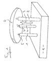
- FIG. 1 shows a movement device for a raster tunnel microscope (RTM) consisting of three movement elements 1, 2, 3 with a raster element 4 arranged here centrally between the movement elements 1, 2, 3 for measuring the tunnel current.
- RTM raster tunnel microscope
- the movement elements 1, 2, 3 are arranged at the same distance from one another. All movement elements 1, 2, 3 and the grid element 4 have the same structure.
- cylindrical parts made of piezoelectric material, for example piezoceramic were used for the formation of the elements, the movement elements on the end face having a support 5 for a part to be examined with the RTM Object 6 and the raster element 4 are provided with a scanning needle 7 (tunnel tip).
- the movement elements 1, 2, 3 and the grid element 4 are attached to a common base plate 8 in the exemplary embodiment.
- Varyable stresses or voltage profiles can be applied to each of the elements or by continuously changing the voltages, which cause a shortening or lengthening or bending of the ceramic material.
- the object 6 rests on the supports 5 of the movement elements 1, 2, 3 that are spherical in the exemplary embodiment. This three-point support of the object 6 ensures a stable support for the object. If this cannot be achieved solely by the action of gravity, the object can also be pressed onto the supports 5 of the movement elements by means of spring force.
- FIG. 2 shows a movement element with an attached support 5 in a perspective view.
- a cross section of the movement element is shown in Figure 2a.
- a tube 9 made of piezoceramic material was used to form the movement element.
- the piezoceramic tube has an outside diameter of 2 mm and an inside diameter of 1 mm.
- the piezoceramic tube 9 is provided with a closed, electrically conductive coating 10 as the inner electrode.
- the outer cylinder wall of the movement element carries four electrically conductive partial coverings 11 to 14, which are electrically insulated from one another as strip electrodes by means of insulations 15.
- the partial coverings 11 to 14 are laid on the outer cylinder wall parallel to the axis 16 of the movement element, the insulations 15 run in the axial direction.
- the piezoelectric material is radially polarized, as is marked by arrows 17 in FIG. 2a.
- Electrical lines 18 to 22 are connected to the inner covering 10 and to the partial coverings 11 to 14, via which voltages or voltage profiles can be applied to the moving element.
- the voltages required for the movements of the movement element in the X, Y and Z directions are generated by a controllable voltage transmitter 23.
- the movement element deforms in the axial direction, ie it lengthens or shortens in the Z direction, depending on the polarity of the applied voltage.
- a voltage is applied between the individual partial coverings and the inner cover 10 of the piezoelectric tube 9
- the free end of the movement element with the support 5 bends perpendicular to its axis 16 in the X or Y direction.
- the deflection is increased when voltages of opposite polarity between the opposite on the outer cylinder wall Partial coverings are created, for example between the partial coverings 11 and 13 or 12 and 14, the inner covering 10 being at zero potential.
- the movement element By superimposing the aforementioned voltages, the movement element can thus be deformed in such a way that the support 5 executes every movement required for a desired change in the position of the object, the operating voltages required for this being relatively small because of the dimensions and thin-walled design of the movement element.
- the movement elements 1, 2, 3 and the raster element 4 are adjusted in their level to one another in the base plate 8 so that the scanning needle 7 of the pushbutton element is at a sufficiently small distance from the object surface to be examined when the object 6 is placed on the supports 5 of the movement elements .
- a fine adjustment of the distance between the scanning needle and the object surface is then carried out by applying a corresponding voltage to movement elements and / or to the grid element.
- the arrangement of movement elements and grid element on the same base plate and the identical design selected for the movement elements and the grid element from the same piezoceramic material and with the same dimensions lead to the same thermal expansion behavior for movement elements and grid element, so that the temperature expansion is compensated between the object surface and the grid element.
- FIG. 3 shows schematically two possible movement sequences for the movement elements:
- Steps b and c can be repeated as long as necessary until the object has reached the desired working position for the RTM examination. This is followed by step d for moving the object to the scanning needle 7.
- Each of the movement sequences shown in FIGS. 3a and 3b can be carried out continuously in steps that repeat continuously, either individually or with a voltage pulse sequence applied to the movement elements.
- the step size and step frequency of the supports of the movement elements can be varied within wide limits by appropriate choice of voltage amplitude and pulse frequency. With the piezoelectric movement elements, steps with a step size of less than 10 nm can be carried out reproducibly.
- the movement sequences that can be carried out with the movement elements are not limited to the movements shown in FIGS. 3a and 3b. Rather, the movement of the movement elements can be adapted to the respective application. For example, in addition to the movement sequences described above, elliptical movements of the supports or a throwing up of the object with a rapid change of location of the supports are also possible.
- the motion sequences are controlled taking into account the inertia of the object.
- the movement device there is also a rotation of the objects about an axis possible perpendicular to the support plane.
- the objects are rotated by corresponding vectorial addition of the voltages in the X and Y directions for each individual movement element.
- the objects can also be tilted.
- the individual movement elements are to be stretched or shortened differently.
- the movement device thus also allows the objects to be rotated and tilted.
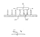
- FIG. 4 shows a transport table 24 with a plurality of movement elements 25 arranged adjacent to one another.
- the movement elements are at such a distance from one another that the object to be moved is supported in every position by at least three movement elements and can be moved in any manner on the transport table 24.
- FIG. 5 shows a perspective view of a raster element 4 of the movement device shown in FIG. 1 for an RTM.
- the grid element is designed in the same way as a movement element. It has a tube 26 made of the same, radially polarized piezoelectric material as the tube 9 in FIG. 2 and is on its inner cylinder wall with a closed, electrically conductive coating 27 as an inner electrode and on its outer cylinder wall provided with electrically conductive partial coverings 28 to 31, between each of which an insulation layer 32 runs in the axial direction.
- the scanning needle 7 is used instead of a support 5 for the raster element 4.
- FIG. 5 also shows schematically the electrical connections for the raster element 4.
- the tunnel current tapped in the operating case by the scanning needle 7 is discharged via an electrical line 33 connected to the scanning needle 7 and amplified in an amplifier 34.
- the output voltage of the amplifier is used to move the grid element in the Z direction (axis direction).
- Two ramp generators 35, 36 are used to control the scanning needle in the X and Y planes.
- the base potential of these generators can be superimposed by an adjustable voltage for the Z direction.
- the output of the ramp generator 35 is connected to the partial coverings 28 and 30 via connections 37, 38, and the output of the ramp generator 36 is connected to the partial coverings 29, 31 of the grid element via connections 39, 40.
- the inner closed coating 27, the inner electrode is connected to earth potential in the exemplary embodiment. In this way, the inner electrode can also serve as a shield for the electrical line 33.
- FIG. 6 shows the electrical line 33 running inside the raster element, which is connected to the scanning needle 7.
- the amplification and recording of the tunnel current is carried out in the manner known from RTM's.
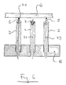
- the temperature of the object surface can be measured via a thermal sensor 41, which is installed in one of the movement elements, in the exemplary embodiment in movement element 3 (see FIG. 6).
- a thermocouple is provided as a temperature sensor, which is inserted into the support 5.
- FIG. 6 also shows a moving element, in the exemplary embodiment the moving element 2, in the cavity of which a potential supply 42 is laid.
- the potential supply 42 is connected to the support 5 of the movement element.
- the electrical potential of the object which is placed on the movement element 2 can be set accordingly via the potential supply.
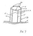
- FIG. 7 Another exemplary embodiment of a movement element is shown in FIG. 7.
- the construction of the movement element 50 is similar to that of the movement element shown in FIG. 2.
- the movement element 50 instead of the support 5 in FIG. 2, the movement element 50 has three hemispherical support supports 52 on the upper end face 51 thereof.
- the dimensions of the movement element 50 are selected in such a way that a stable object position is achieved when an object is placed on the support supports 52.
- the movement element 50 can thus also be used as an individual object support instead of the three movement elements shown in FIG. 1.
- FIGS. 8 and 8a show a further movement element 53, which has three outer electrodes 54 to 56 distributed over the circumference. in the otherwise it shows the same structure as the movement element shown in FIG. 2. All movements can also be carried out with the movement element 53, as shown in FIGS. 3a and 3b.
- the respective direction of movement of the movement element or that of the support 5 for the object follows from the electrical voltages which are applied to the three electrodes.
- the movement device described in the exemplary embodiment cannot only be used for object movement in the RTM. It can of course also be used for object manipulation in any type of micro movement, both in microscopic examinations and in the processing of objects in microtechnology. If it is used, for example, in microlithography, the movement device is merely to be equipped with an element corresponding to the processing instead of with a scanning needle. In addition, the structure of the movement device can in principle be kept unchanged.
- the movement device of the type described is not only able to analyze atomic structures according to the RTM method, but also to generate structures with lateral resolutions in the nm range. In the simplest case, such an arrangement can - as already described above - be carried out similarly to the RTM.
- the object to be processed rests on at least 3 support elements.
- a suitable "processing tool” can be mounted on one or more other movement elements (instead of the scanning needle used in the RTM).
- This processing tool can consist, for example, of a sharp tip (e.g. diamond tip), which can be guided over the object surface to be machined when the movement device is appropriately activated, and in this way digs holes and structures on this surface.
- the movement elements are expediently computer-controlled. The operations can thus be carried out with high speed and precision. Since the device described can be used to transport objects of any size in microtechnology over large distances and since several movement elements can be used and operated in parallel with processing tools, a large area (e.g. a semiconductor wafer of large dimensions) can be provided with microstructures at the same time.
- Suitable as another processing tool that can be mounted on a moving element a field emission peak. It can be used to locally activate surface atoms of an object by electron emission or ion emission or even only due to high electrical fields. This process is used, for example, for the local cracking of hydrocarbon compounds, which leads to a chemical conversion of the "processed" molecule.
- Another application example for the described movement device with processing element is its use in microbiology.
- Organic molecular chains, viruses or bacteria can not only be analyzed, but also by using local fields at targeted points, a separation or modification of the molecular chains can be brought about. This possibility of a targeted operation in the molecular area opens up completely new possibilities also in the field of genetic engineering.
- Another possibility is to use the movement element similar to a "MOUSE”, as they are known as electronic scanning devices.
- the object to be processed remains agitated while the moving element moves over the object.
Landscapes
- Chemical & Material Sciences (AREA)
- Radiology & Medical Imaging (AREA)
- Engineering & Computer Science (AREA)
- Nuclear Medicine, Radiotherapy & Molecular Imaging (AREA)
- Nanotechnology (AREA)
- Physics & Mathematics (AREA)
- Health & Medical Sciences (AREA)
- General Health & Medical Sciences (AREA)
- General Physics & Mathematics (AREA)
- Crystallography & Structural Chemistry (AREA)
- Analytical Chemistry (AREA)
- Manipulator (AREA)
- Measurement Of Length, Angles, Or The Like Using Electric Or Magnetic Means (AREA)
- General Electrical Machinery Utilizing Piezoelectricity, Electrostriction Or Magnetostriction (AREA)
- Length Measuring Devices With Unspecified Measuring Means (AREA)
- Details Of Measuring And Other Instruments (AREA)
- Microscoopes, Condenser (AREA)
- Control And Other Processes For Unpacking Of Materials (AREA)
- Ultra Sonic Daignosis Equipment (AREA)
- Apparatus Associated With Microorganisms And Enzymes (AREA)
Abstract
Description
Die Erfindung bezieht sich auf eine Bewegungseinrichtung für rastermikroskopisch zu untersuchende Objekte mit piezoelektrisch bewegbarer Rasternadel.The invention relates to a movement device for objects to be examined by scanning microscopy with a piezoelectrically movable scanning needle.
Bei Untersuchungen mit dem Raster-Tunnel-Mikroskop (RTM) von G. Binnig und H. Rohrer sind sehr präzise Mikrobewegungen der Objekte notwendig, vgl. Helvetia Phys. Acta 55, 1982, S. 726. Das RTM erfordert ein Höchstmaß an Präzision und Stabilität für die Bewegung des jeweils zu untersuchenden Objektes. Sowohl für das Abrastern des Objektes als auch für die Objektmanipulation sind Präzisionsbewegungen im Nanometerbereich für das Erzielen gewünschter Ergebnisse Voraussetzung, wobei die Bewegungen zuverlässig, reproduzierbar und rasch durchgeführt und gesteuert werden müssen.Examinations with the scanning tunnel microscope (RTM) by G. Binnig and H. Rohrer require very precise micro movements of the objects, cf. Helvetia Phys. Acta 55, 1982, p. 726. The RTM requires maximum precision and stability for the movement of the object to be examined. Precision movements in the nanometer range are a prerequisite for achieving the desired results, both for scanning the object and for object manipulation, the movements having to be carried out and controlled reliably, reproducibly and quickly.
Die bisher bekannten Stellelemente für RTM's verwenden eine Kombination von drei piezoelektrischen Stellgliedern für die Rasterung (ein Dreibein mit je einem Stellglied in den drei Koordinatenrichtungen x, y, z) und weitere Stellglieder für die Objektmanipulation, die entweder piezoelektrisch, elektronmagnetisch oder mechanisch arbeiten, G. Binning und H. Rohrer, "Das Raster-Tunnelmikroskop", Spektrum der Wissenschaft, 1985, S. 62/68; J. Moreland et al, "Electromagnetic Squeezer for Compressing Squeezable Electron Tunnel Junctions", Rev. Sci. Instrum. 53, 1984, S. 399. Diese in ihrem Aufbau komplexen Stellelemente sind störanfällig, Vibration und Temperaturdrift lassen sich kaum vermeiden. Kritisch sind auch die für den Betrieb der Piezokeramiken notwendigen hohen Spannungen.The previously known actuators for RTM's use a combination of three piezoelectric actuators for rasterization (a tripod with one actuator each in the three coordinate directions x, y, z) and further actuators for object manipulation, which work either piezoelectrically, electronically or mechanically, G Binning and H. Rohrer, "The scanning tunneling microscope", Spectrum of Science, 1985, pp. 62/68; J. Moreland et al, "Electromagnetic Squeezer for Compressing Squeezable Electron Tunnel Junctions," Rev. Sci. Instrument. 53, 1984, p. 399. These control elements, which are complex in their construction, are prone to failure, Vibration and temperature drift can hardly be avoided. The high voltages required to operate the piezoceramics are also critical.
Aufgabe der Erfindung ist es, eine Einrichtung für Bewegungsabläufe zu schaffen, die sich durch hohe Stabilität, eine präzise Steuerung der Bewegung, einfachen Aufbau, geringe Vibrationsanfälligkeit und geringe Temperaturdrift auszeichnet.The object of the invention is to provide a device for motion sequences, which is characterized by high stability, precise control of the movement, simple structure, low susceptibility to vibration and low temperature drift.
Diese Aufgabe wird bei einer Bewegungseinrichtung der eingangs angegebenen Art durch die in Patentanspruch 1 angegebenen Merkmale gelöst. Danach ist das Objekt auf drei gleichartig ausgebildeten piezoelektrisch einstellbaren Bewegungselementen gelagert, die das Objekt abstützen. Die Bewegungselemente sind mit der Rasternadel des RTM's ortsfest verbunden. Die Bewegungselemente werden durch Anlegen elektrischer Spannung am piezoelektrischen Material verformt. Durch Variation der Spannung lassen sich die Bewegungselemente in ihrer Lage jeweils derart verändern, daß sich das von den Bewegungselementen abgestützte Objekt in einer gewünschten Richtung innerhalb der durch Auflage des Objekts auf den Bewegungselementen vorgegebenen Ebene bewegt. Diese Bewegung kann rein translatorisch sein, das Objekt kann von den Bewegungselementen aber auch um eine Achse gedreht oder gekippt werden. Hierzu ist jedes piezoelektrische Bewegungselement gesondert ansteuerbar.This object is achieved in a movement device of the type specified by the features specified in
Die Bewegungselemente sind hohlzylinderartig ausgebildet und stirnseitig mit einer Auflage für das Objekt versehen. Ein solches zylindrisches Bewegungselement weist eine hohe mechanische Steifigkeit auf. Zur Ansteuerung der Bewegungselemente sind auf einer ihrer Zylinderwände ein geschlossener elektrisch leitfähiger Belag und auf ihrer anderen Zylinderwand mehrere, gegeneinander elektrisch isolierte, elektrisch leitfähige Teilbeläge angeordnet. Die gegeneinander isolierten Teilbeläge erstrecken sich in Richtung der Zylinderachse des Bewegungselements. Durch Anlegen einer Spannung zwischen den Belägen auf beiden Zylinderwänden wird eine Verkürzung oder Dehnung des Bewegungselementes erreicht. Zum Verbiegen des Bewegungselementes ist eine Spannung zwischen den geschlossenen Belag und einem Teilbelag anzulegen. Solche Bewegungselemente sind aus US-A-4 087 715 bekannt.The movement elements are designed like hollow cylinders and are provided with a support for the object on the end face. Such a cylindrical movement element has a high mechanical rigidity. To control the movement elements are on one of them Cylinder walls a closed electrically conductive covering and arranged on their other cylinder wall several, electrically insulated, electrically conductive partial coverings. The mutually insulated partial coverings extend in the direction of the cylinder axis of the movement element. By applying a tension between the pads on both cylinder walls, the movement element is shortened or stretched. To bend the movement element, a tension must be applied between the closed covering and a partial covering. Such movement elements are known from US-A-4 087 715.
Man kann somit durch Überlagerung der angelegten Spannungen alle für die Bewegung des Objektes erforderlichen Lageveränderungen ausführen, wobei die hierfür notwendigen elektrischen Spannungen wegen der mit verhältnismäßig geringer Wandstärke ausführbaren Bewegungselementen entsprechend klein gehalten werden können.Thus, by superimposing the applied voltages, all changes in position required for the movement of the object can be carried out, the electrical voltages required for this being able to be kept correspondingly small because of the movement elements which can be implemented with a relatively small wall thickness.
Die starre Verbindung zwischen Bewegungselementen und Rasterelement führt zu einer geschlossenen kompakten Baueinheit mit hoher mechanischer Stabilität und Temperaturunempfindlichkeit bei der Raster-Tunnel-Mikroskopie. Nach Patentanspruch 2 ist das Rasterelement in gleicher Weise wie ein Bewegungselement ausgebildet. Es besteht somit insbesondere aus hohlzylindrischem piezoelektrischen Material, das auf seiner inneren und äußeren Zylinderwand mit elektrisch leitenden Belägen bzw. Teilbelägen versehen ist. Diese analoge Ausbildung von Rasterelement und Bewegungselementen führt beim Einsatz der Bewegungseinrichtung bei einem RTM zu weitgehender Vibrationsfreiheit und zur Kompensation der Temperaturdrift. Der gleiche Aufbau von Bewegungselementen und Rasterelement ermöglicht es auch, die für die RTM-Anwendung notwendige Rasterbewegung statt mit dem Rasterelement mit den Bewegungselementen auszuführen. Zur Temperaturmessung des Objekts ist zumindest eines der Bewegungselemente mit einem Thermofühler ausgestattet, Patentanspruch 3.The rigid connection between motion elements and raster element leads to a closed, compact unit with high mechanical stability and insensitivity to temperature in raster tunnel microscopy. According to
Aus herstellungstechnischen Gründen sind die gegeneinander isolierten, elektrisch leitenden Teilbeläge bevorzugt auf der äußeren Zylinderwand eines Bewegungselementes angeordnet, Patentanspruch 4.For manufacturing reasons, the electrically conductive partial coverings which are insulated from one another are preferably arranged on the outer cylinder wall of a movement element.
Eine optimale elektrische Steuerung der Bewegungselemente ist nach Patentansprüchen 5 und 6 dann gegeben, wenn jeder elektrisch leitende Belag auf den Zylinderflächen eines Bewegungselementes gesondert ansteuerbar ist. Die Objektbewegung läßt sich dann jeweils durch unterschiedliche elektrische Betriebsspannungen an den Belägen optimal regulieren. Eine Justierung der Ruhelage der Bewegungselemente läßt sich durch Anlegen einer Gleichspannung erreichen, die von der für den Betrieb erforderlichen Wechselspannung überlagert wird.An optimal electrical control of the movement elements is given according to
Die Erfindung und weitere Erfindungsmerkmale werden im folgenden anhand von Ausführungsbeispielen näher erläutert. Die Zeichnung zeigt im einzelnen:
Figur 1- Bewegungseinrichtung als Objektträger und Rasterelement bei einem Raster-Tunnel-Mikroskop (RTM);
Figur 2- Bewegungselement in perspektivischer Darstellung und im Querschnitt (Figur 2a);
Figur 3- Bewegungsabläufe der Bewegungselemente bei einer Objektmanipulation: mit vom Objekt abhebendem Bewegungselement (Fig. 3a) mit rutschender Bewegung des Bewegungselementes auf der Objektoberfläche (Fig. 3b);
Figur 4- Transporteinrichtung zur Mikrobewegung von Objekten über eine größere Distanz;
Figur 5- Rasterelement in perspektivischer Darstellung und im Querschnitt (Fig. 5a);
Figur 6- Bewegungselemente mit Thermofühler und Potentialzuführung sowie Rasterelement im Längsschnitt;
Figur 7- Bewegungselement in perspektivischer Darstellung mit Auflagestützen für das Objekt;
Figur 8- Bewegungselement mit drei Außenelektroden in perspektivischer Darstellung und im Querschnitt (Fig. 8a).
- Figure 1
- Movement device as slide and raster element in a raster tunnel microscope (RTM);
- Figure 2
- Movement element in perspective and in cross section (Figure 2a);
- Figure 3
- Movement sequences of the movement elements in the case of object manipulation: with a movement element lifting off the object (FIG. 3a) with a sliding movement of the movement element on the object surface (FIG. 3b);
- Figure 4
- Transport device for micro-movement of objects over a greater distance;
- Figure 5
- Raster element in perspective and in cross section (Fig. 5a);
- Figure 6
- Movement elements with thermal sensor and potential supply as well as raster element in longitudinal section;
- Figure 7
- Movement element in perspective with support supports for the object;
- Figure 8
- Movement element with three outer electrodes in perspective and in cross section (Fig. 8a).
Figur 1 zeigt eine aus drei Bewegungselementen 1, 2, 3 bestehende Bewegungseinrichtung für ein Raster-Tunnel-Mikroskop (RTM) mit einem hier zentral zwischen den Bewegungselementen 1, 2, 3 angeordnetem Rasterelement 4 zur Messung des Tunnelstroms. Die Bewegungselemente 1, 2, 3 sind im Ausführungsbeispiel in gleichem Abstand zueinander angeordnet. Alle Bewegungselemente 1, 2, 3 und das Rasterelement 4 weisen den gleichen Aufbau auf. Für die Ausbildung der Elemente wurden im Ausführungsbeispiel zylinderförmige Teile aus piezoelektrischem Material, beispielsweise Piezokeramik, verwendet, wobei die Bewegungselemente stirnseitig mit einer Auflage 5 für ein mit dem RTM zu untersuchendes Objekt 6 und das Rasterelement 4 mit einer Abtastnadel 7 (Tunnelspitze) versehen sind. Die Bewegungselemente 1, 2, 3 und das Rasterelement 4 sind im Ausführungsbeispiel an einer gemeinsamen Grundplatte 8 befestigt. An jedes der Elemente sind variierbare Spannungen bzw. durch stetiges Verändern der Spannungen Spannungsverläufe anlegbar, die eine Verkürzung oder Verlängerung oder ein Verbiegen des keramischen Materials bewirken.FIG. 1 shows a movement device for a raster tunnel microscope (RTM) consisting of three
Das Objekt 6 ruht auf den im Ausführungsbeispiel kugelförmig ausgebildeten Auflagen 5 der Bewegungselemente 1, 2, 3. Durch diese Dreipunktunterstützung des Objektes 6 ist eine stabile Auflage für das Objekt gewährleistet. Ist dies allein durch Schwerkraftwirkung nicht zu erreichen, kann das Objekt auch mittels Federkraft auf die Auflagen 5 der Bewegungselemente aufgedrückt werden.The
Der Aufbau eines Bewegungselementes 1, 2 oder 3 wird anhand von Figur 2 erläutert. Figur 2 zeigt ein Bewegungselement mit aufgesetzter Auflage 5 in perspektivischer Darstellung. Ein Querschnitt des Bewegungselementes ist in Figur 2a wiedergegeben. Für die Ausbildung des Bewegungselementes wurde ein Rohr 9 aus piezokeramischen Material verwendet. Im Ausführungsbeispiel weist das piezokeramische Rohr einen Außendurchmesser von 2 mm und einen Innendurchmesser von 1 mm auf. Auf seiner inneren Zylinderwand ist das piezokeramischen Rohr 9 mit einem geschlossenen, elektrisch leitfähigen Belag 10 als Innenelektrode versehen. Die äußere Zylinderwand des Bewegungselementes trägt vier elektrisch leitfähige Teilbeläge 11 bis 14, die als Streifenelektroden mittels Isolationen 15 gegeneinander elektrisch isoliert sind. Die Teilbeläge 11 bis 14 sind auf der äußeren Zylinderwand parallel zur Achse 16 des Bewegungselementes verlegt, die Isolationen 15 verlaufen in Achsrichtung. Im Ausführungsbeispiel ist das piezoelektrische Material radial polarisiert, wie es in Figur 2a durch Pfeile 17 markiert ist.The structure of a
Am inneren Belag 10 und an den Teilbelägen 11 bis 14 sind elektrische Leitungen 18 bis 22 angeschlossen, über die am Bewegungselement Spannungen bzw. Spannungsverläufe anlegbar sind. Die erforderlichen Spannungen für die Bewegungen des Bewegungselementes in X-, Y-, Z-Richtung werden von einem regelbaren Spannungsgeber 23 erzeugt.
Werden alle Teilbeläge 11 bis 14 auf gleiches elektrisches Potential gebracht und wird zwischen diesen und dem inneren Belag 10 eine Spannungsdifferenz angelegt, so deformiert sich das Bewegungselement in Achsrichtung, d.h. es verlängert oder verkürzt sich in Z-Richtung, je nach Polarität der angelegten Spannung. Wird jedoch zwischen einzelnen Teilbelägen und innerem Belag 10 des piezoelektrischen Rohres 9 eine Spannung angelegt, so verbiegt sich das freie Ende des Bewegungselementes mit der Auflage 5 senkrecht zu seiner Achse 16 in X- oder Y-Richtung. Die Verbiegung wird verstärkt, wenn Spannungen entgegengerichteter Polarität zwischen den auf der aüßeren Zylinderwand gegenüberliegenden Teilbelägen angelegt werden, also beispielsweise zwischen den Teilbelägen 11 und 13 oder 12 und 14, wobei der innere Belag 10 auf Potential Null liegt.If all of the
Durch Überlagern der vorgenannten Spannungen läßt sich das Bewegungselement somit derartig verformen, daß die Auflage 5 jede für eine gewünschte Lagerveränderung des Objekts erforderliche Bewegung ausführt, wobei die hierfür notwendigen Betriebsspannungen wegen der Abmessungen und dünnwandigen Ausführung des Bewegungselementes relativ klein sind.By superimposing the aforementioned voltages, the movement element can thus be deformed in such a way that the
Die Bewegungselemente 1, 2, 3 und das Rasterelement 4 sind in ihrem Niveau zueinander in der Grundplatte 8 so justiert, daß die Abtastnadel 7 des Tasterelementes bei Auflegen des Objektes 6 auf die Auflagen 5 der Bewegungselemente einen hinreichend geringen Abstand von der zu untersuchenden Objektoberfläche aufweist. Eine Feineinstellung des Abstandes zwischen Abtastnadel und Objektoberfläche wird dann durch Anlegen einer entsprechenden Spannung an Bewegungselementen und/oder am Rasterelement vorgenommen. Die Anordnung von Bewegungselementen und Rasterelement auf derselben Grundplatte und die für die Bewegungselemente und das Rasterelement gewählte identische Ausbildung aus gleichem piezokeramischen Material und mit gleicher Abmessung führen für Bewegungselemente und Rasterelement zu gleichem thermischen Ausdehnungsverhalten, so daß zwischen Objektoberfläche und Rasterelement die Temperaturausdehnung kompensiert wird.The
Um eine Verschiebung oder Drehung des Objektes zu erreichen, zeigt Figur 3 schematisch zwei mögliche Bewegungsabläufe für die Bewegungselemente:In order to achieve a displacement or rotation of the object, FIG. 3 shows schematically two possible movement sequences for the movement elements:
Figur 3a zeigt einen Bewegungsablauf, bei dem zum Transport eines Objektes von einem Punkte A bis zu einem Punkte B die Auflage 5 eines Bewegungselementes in vier aufeinanderfolgenden Arbeitsschritten wie folgt bewegt wird:
- a) Durch synchrones und einheitliches Verlängern aller drei Bewegungselemente 1, 2, 3 wird das Objekt im ersten Schritt a zunächst in Z-Richtung aus der Arbeitsposition der Abtastnadel 7 abgehoben.
- b) Im zweiten Schritt b werden die Bewegungselemente in Z-Richtung rasch abgesenkt, dabei in der X-Y-Ebene geschwenkt und wieder angehoben, so daß sich als Bewegungslinie etwa eine Halbkreisbahn ergibt. Dieser zweite Schritt b wird in seinem Ablauf so gesteuert, daß die Geschwindigkeit des Absenkens der Auflage 5 in Z-Richtung größer ist als eine Bewegung des Objektes in gleicher Richtung unter Einwirkung der Schwerkraft.
Die Auflagen 5 der Bewegungselemente lösen sich bei diesem zweiten Arbeitsschritt im Punkt A vom Objekt, das aufgrund seiner Trägkeit praktisch in seiner Position verharrt, und unterstützen es am Ende des Arbeitsschrittes im Punkt B erneut. - c) Als dritter Schritt c folgt dann eine langsame Bewegung der Auflage 5 in der X-Y-Ebene, wobei das Objekt auf den drei Bewegungselementen ruhen bleibt und in Richtung der Bewegung der Bewegungselemente um eine Strecke transportiert wird, die dem Abstand zwischen den Punkten A und B entspricht.
- d) Um wieder in die Arbeitsposition für die
Abtastnadel 7 zu gelangen, bedarf es als vierten Arbeitsschritt d noch einer Absenkung des Objektes in Z-Richtung. Am Ende dieses Arbeitsschrittes befinden sich die Bewegungselemente wieder in ihrer Ausgangsposition und das Objekt ist um die Strecke zwischen den Punkten A und B verschoben worden.
- a) By synchronously and uniformly extending all three
movement elements scanning needle 7 in the first step a. - b) In the second step b, the movement elements are quickly lowered in the Z direction, pivoted in the XY plane and raised again, so that there is approximately a semicircular path as the movement line. The sequence of this second step b is controlled such that the speed of lowering the
support 5 in the Z direction is greater than a movement of the object in the same direction under the influence of gravity. Thesupports 5 of the movement elements detach from the object in this second step in point A, which practically remains in position due to its inertia, and support it again in point B at the end of the step. - c) The third step c is followed by a slow movement of the
support 5 in the XY plane, with the object on the three movement elements remains at rest and is transported in the direction of the movement of the movement elements by a distance which corresponds to the distance between points A and B. - d) In order to return to the working position for the
scanning needle 7, a fourth step d requires a lowering of the object in the Z direction. At the end of this step, the movement elements are back in their starting position and the object has been moved by the distance between points A and B.
Die Arbeitsschritte b und c lassen sich beliebig wiederholen, so lange, bis das Objekt die für die RTM-Untersuchung gewünschte Arbeitsstellung erreicht hat. Anschließend erfolgt dann Arbeitsschritt d zum Heranführen des Objekts an die Abtastnadel 7.Steps b and c can be repeated as long as necessary until the object has reached the desired working position for the RTM examination. This is followed by step d for moving the object to the
Ein gegenüber dem vorbeschriebenen Verfahren vereinfachter Bewegungsablauf für die Bewegungselemente ist in Figur 3b wiedergegeben. Die Bewegungselemente werden danach in nur zwei Arbeitsschritten gesteuert:
- a) Als erster Schritt a erfolgt eine schnelle Bewegung der Auflage 5 auf der Objektoberfläche vom Punkt A nach Punkt B. Bei dieser Bewegung der Bewegungselemente bleibt das Objekt aufgrund seiner Massenträgheit wieder in nahezu unveränderter Position.
- b) Beim zweiten Schritt b wird das Bewegungselement in seine Ausgangsposition zurückgeholt, wobei das Objekt bei langsamer Bewegung des Bewegungselementes um die zwischen den Punkten A und B liegende Strecke transportiert wird.
- a) The first step a is a rapid movement of the
support 5 on the object surface from point A to point B. With this movement of the movement elements, the object remains in an almost unchanged position due to its inertia. - b) In the second step b, the movement element is brought back into its starting position, the object being transported by the distance between points A and B when the movement element is moving slowly.
Jeder der in Fig. 3a und 3b wiedergegebene Bewegungsablauf kann einzeln oder bei einer an den Bewegungselementen angelegten Spannungsimpulsfolge in Schritten, die sich kontinuierlich wiederholen, fortlaufend durchgeführt werden. Schrittweite und Schrittfrequenz der Auflagen der Bewegungselemente lassen sich in weiten Grenzen durch entsprechende Wahl von Spannungsamplitude und Impulsfrequenz variieren. Mit den piezoelektrischen Bewegungselementen lassen sich Schritte mit einer Schrittweite von weniger als 10 nm reproduzierbar ausführen.Each of the movement sequences shown in FIGS. 3a and 3b can be carried out continuously in steps that repeat continuously, either individually or with a voltage pulse sequence applied to the movement elements. The step size and step frequency of the supports of the movement elements can be varied within wide limits by appropriate choice of voltage amplitude and pulse frequency. With the piezoelectric movement elements, steps with a step size of less than 10 nm can be carried out reproducibly.
Die mit den Bewegungselementen ausführbaren Bewegungsabläufe sind auf die in Fig. 3a und 3b wiedergegebenen Bewegungen nicht beschränkt. Vielmehr läßt sich die Bewegung der Bewegungselemente dem jeweiligen Anwendungsfall entsprechend anpassen. Beispielsweise sind neben den vorbeschriebenen Bewegungsabläufen auch ellipsenförmige Bewegungen der Auflagen oder ein Hochwerfen des Objekts mit schnellem Ortswechsel der Auflagen möglich. Die Steuerung der Bewegungsabläufe erfolgt dabei unter Berücksichtigung der Massenträgheit des Objekts.The movement sequences that can be carried out with the movement elements are not limited to the movements shown in FIGS. 3a and 3b. Rather, the movement of the movement elements can be adapted to the respective application. For example, in addition to the movement sequences described above, elliptical movements of the supports or a throwing up of the object with a rapid change of location of the supports are also possible. The motion sequences are controlled taking into account the inertia of the object.
Mit der beschriebenen Bewegungseinrichtung ist auch eine Drehung der Objekte um eine Achse senkrecht zur Auflagenebene möglich. Das Drehen der Objekte erfolgt durch entsprechende vektorielle Addition der Spannungen in X- und Y-Richtung für jedes einzelne Bewegungselement. Darüberhinaus lassen sich die Objekte auch kippen. Hierzu sind die einzelnen Bewegungselemente unterschiedlich zu strecken oder zu verkürzen. Die Bewegungseinrichtung erlaubt somit neben translatorischen Bewegungen auch ein Drehen und Kippen der Objekte.With the described movement device, there is also a rotation of the objects about an axis possible perpendicular to the support plane. The objects are rotated by corresponding vectorial addition of the voltages in the X and Y directions for each individual movement element. The objects can also be tilted. For this purpose, the individual movement elements are to be stretched or shortened differently. In addition to translational movements, the movement device thus also allows the objects to be rotated and tilted.
Mit den Bewegungselementen der angegebenen Art können Objekte aber auch über weitere Entfernung mit hoher Präzision transportiert werden. Einen Transporttisch 24 mit mehreren benachbart zueinander angeordneten Bewegungselementen 25 zeigt Figur 4. Die Bewegungselemente weisen untereinander einen solchen Abstand auf, daß das zu bewegende Objekt in jeder Position zumindest von drei Bewegungselementen gestützt ist und in beliebiger Weise auf dem Transporttisch 24 verschoben werden kann.With the movement elements of the specified type, objects can also be transported over great distances with high precision. FIG. 4 shows a transport table 24 with a plurality of
Figur 5 zeigt in perspektivischer Darstellung ein Rasterelement 4 der in Figur 1 gezeigten Bewegungseinrichtung für ein RTM. Das Rasterelement ist in gleicher Weise wie ein Bewegungselement ausgebildet. Es weist ein Rohr 26 aus demselben, radial polarisiertem piezoelektrischen Material auf wie das Rohr 9 in Fig. 2 und ist auf seiner inneren Zylinderwand mit einem geschlossenen, elektrisch leitfähigen Belag 27 als Innenelektrode und auf seiner äußeren Zylinderwand mit elektrisch leitfähigen Teilbelägen 28 bis 31 versehen, zwischen denen in axialer Richtung jeweils eine Isolationsschicht 32 verläuft. Im Gegensatz zu einem Bewegungselement ist jedoch statt einer Auflage 5 beim Rasterelement 4 die Abtastnadel 7 eingesetzt.FIG. 5 shows a perspective view of a
Figur 5 zeigt schematisch auch die elektrischen Anschlüsse für das Rasterelement 4. Der im Betriebsfall von der Abtastnadel 7 abgegriffene Tunnelstrom wird über eine an der Abtastnadel 7 angeschlossene elektrische Leitung 33 abgeführt und in einem Verstärker 34 verstärkt. Die Ausgangsspannung des Verstärkers wird zur Bewegung des Rasterelementes in Z-Richtung (Achsrichtung) benutzt.FIG. 5 also shows schematically the electrical connections for the
Für die Steuerung der Abtastnadel in der X-und Y-Ebene dienen zwei Rampengeneratoren 35, 36. Das Basispotential dieser Generatoren ist überlagerbar durch eine regulierbare Spannung für die Z-Richtung. Im Ausführungsbeispiel ist der Ausgang des Rampengenerators 35 über Anschlüsse 37, 38 mit den Teilbelägen 28 und 30, der Ausgang des Rampengenerators 36 über Anschlüsse 39, 40 mit den Teilbelägen 29, 31 des Rasterelementes verbunden. Der innere geschlossene Belag 27, die Innenelektrode, ist im Ausführungsbeispiel auf Erdpotential gelegt. Auf diese Weise kann die Innenelektrode zugleich als Abschirmung für die elektrische Leitung 33 dienen. Figur 6 zeigt die im Inneren des Rasterelementes verlaufende elektrische Leitung 33, die mit der Abtastnadel 7 verbunden ist. Die Verstärkung und Aufzeichnung des Tunnelstromes erfolgt in der bei RTM's üblichen, bekannten Weise.Two
Die Temperatur der Objektoberfläche läßt sich über einen Thermofühler 41 messen, der in einem der Bewegungselemente, im Ausführungsbeispiel im Bewegungselement 3 (s. Figur 6), verlegt ist. Im Ausführungsbeispiel ist als Temperaturfühler ein Thermoelement vorgesehen, das in die Auflage 5 eingesetzt ist. In Figur 6 ist auch ein Bewegungselement gezeigt, im Ausführungsbeispiel das Bewegungselement 2, in dessen Hohlraum eine Potentialzuführung 42 verlegt ist. Die Potentialzuführung 42 ist mit der Auflage 5 des Bewegungselementes verbunden. Über die Potentialzuführung ist das elektrische Potential des Objektes, das auf das Bewegungselement 2 aufgelegt wird, entsprechend einstellbar.The temperature of the object surface can be measured via a
Ein weiteres Ausführungsbeispiel für ein Bewegungselement ist in Fig. 7 dargestellt. Das Bewegungselement 50 ist in seinem Aufbau ähnlich dem in Fig. 2 wiedergegebenen Bewegungselement. Es befinden sich jedoch statt der Auflage 5 in Fig. 2 beim Bewegungselement 50 auf dessen oberer Stirnfläche 51 drei halbkugelförmige Auflagestützen 52. Die Abmessungen des Bewegungselementes 50 sind in gewählt, daß beim Auflegen eines Objektes auf die Auflagestützen 52 eine stabile Objektlage erreicht wird. Das Bewegungselement 50 läßt sich somit auch als einzelne Objetstütze statt der in Fig. 1 gezeigten drei Bewegungselemente einsetzen.Another exemplary embodiment of a movement element is shown in FIG. 7. The construction of the movement element 50 is similar to that of the movement element shown in FIG. 2. However, instead of the
In Fig. 8 und 8a ist ein weiteres Bewegungselement 53 gezeigt, das auf dem Umfang verteilt drei Außenelektroden 54 bis 56 aufweist. Im übrigen zeigt es den gleichen Aufbau wie das in Fig. 2 dargestellte Bewegungselement. Auch mit dem Bewegungselement 53 lassen sich alle Bewegungen ausführen, wie sie in Fig. 3a und 3b wiedergegeben sind. Die jeweilige Bewegungsrichtung des Bewegungselementes bzw. die der Auflage 5 für das Objekt folgt aus den elektrischen Spannungen, die an den drei Elektroden angelegt werden.8 and 8a show a further movement element 53, which has three
Die im Ausführungsbeispiel beschriebene Bewegungseinrichtung ist nicht nur für die Objektbewegung beim RTM einsetzbar. Sie kann selbstverständlich darüberhinaus zur Objektmanipulation bei jeder Art von Mikrobewegung, sowohl bei mikroskopischen Untersuchungen als auch bei der Bearbeitung von Objekten in der Mikrotechnik verwendet werden. Wird sie beispielsweise bei der Mikrolithographie eingesetzt, so ist die Bewegungseinrichtung lediglich statt mit einer Abtastnadel mit einem der Bearbeitung entsprechenden Element auszurüsten. Im übrigen kann der Aufbau der Bewegungseinrichtung prinzipiell unverändert beibehalten werden.The movement device described in the exemplary embodiment cannot only be used for object movement in the RTM. It can of course also be used for object manipulation in any type of micro movement, both in microscopic examinations and in the processing of objects in microtechnology. If it is used, for example, in microlithography, the movement device is merely to be equipped with an element corresponding to the processing instead of with a scanning needle. In addition, the structure of the movement device can in principle be kept unchanged.
In der modernen Hochintegrations-Technologie zur Herstellung elektronischer Schaltkreise ist man mit den bisher üblichen Methoden (Photoresistverfahren, Laser-, Elektronen- und Ionensätzen) an einer Grenze angelangt. Zur Erzeugung hoch qualifizierter Strukturen, wie sie für die moderne Mikrochip-Herstellung nötig wären, ist die Bewegungseinrichtung geeignet.In modern high-integration technology for the production of electronic circuits, a limit has been reached with the usual methods (photoresist processes, laser, electron and ion sets). The movement device is suitable for producing highly qualified structures, as would be necessary for modern microchip production.
Die Bewegungseinrichtung der beschriebenen Art ist nicht nur in der Lage, nach dem RTM-Verfahren atomare Strukturen zu analysieren, sondern auch Strukturen mit lateralen Auflösungen im nm-Bereich zu erzeugen. Im einfachsten Fall kann der Aufbau einer solchen Anordnung - wie oben bereits beschrieben - ähnlich wie beim RTM erfolgen. Das zu bearbeitende Objekt ruht wieder auf mindestens 3 Trägerelementen.The movement device of the type described is not only able to analyze atomic structures according to the RTM method, but also to generate structures with lateral resolutions in the nm range. In the simplest case, such an arrangement can - as already described above - be carried out similarly to the RTM. The object to be processed rests on at least 3 support elements.
Auf einem oder auch mehreren weiteren Bewegungselementen kann (statt der beim RTM eingesetzten Abtastnadel) ein geeigentes "Bearbeitungswerkzeug" montiert sein. Dieses Bearbeitungswerkzeug kann beispielsweise aus einer scharfen Spitze (z.B. Diamantspitze) bestehen, die bei entsprechender piezoelektrischer Aktivierung der Bewegungseinrichtung über die zu bearbeitende Objektoberfläche geführt werden kann und auf ihrem Wege Löcher und Strukturen auf dieser Oberfläche gräbt. Die Bewegungselemente werden zweckmäßigerweise computergesteuert. Die Operationen lassen sich somit mit hoher Geschwindigkeit und Präzision durchführen. Da mit der beschriebenen Einrichtung beliebig große Objekte in der Mikrotechnologie über große Distanzen transportiert werden können und da mehrere Bewegungselemente mit Bearbeitungswerkzeugen gleichzeitig parallel eingesetzt und betrieben werden können, kann somit eine große Fläche (z.B. ein Halbleiterwaver großer Dimension) gleichzeitig mit Mikrostrukturen versehen werden.A suitable "processing tool" can be mounted on one or more other movement elements (instead of the scanning needle used in the RTM). This processing tool can consist, for example, of a sharp tip (e.g. diamond tip), which can be guided over the object surface to be machined when the movement device is appropriately activated, and in this way digs holes and structures on this surface. The movement elements are expediently computer-controlled. The operations can thus be carried out with high speed and precision. Since the device described can be used to transport objects of any size in microtechnology over large distances and since several movement elements can be used and operated in parallel with processing tools, a large area (e.g. a semiconductor wafer of large dimensions) can be provided with microstructures at the same time.
Als weiteres Bearbeitungswerkzeug, das an ein Bewegungselement montiert werden kann, eignet sich auch eine Feldemissionsspitze. Mit ihr können durch Elektronenemission oder Ionenemission oder auch nur aufgrund hoher elektrischer Felder Oberflächenatome eines Objektes lokal aktiviert werden. Dieser Vorgang wird z.B. zum lokalen Cracken von Kohlenwasserstoff-Verbindungen angewandt, was zu einer chemischen Umwandlung des "bearbeiteten" Moleküls führt.Suitable as another processing tool that can be mounted on a moving element a field emission peak. It can be used to locally activate surface atoms of an object by electron emission or ion emission or even only due to high electrical fields. This process is used, for example, for the local cracking of hydrocarbon compounds, which leads to a chemical conversion of the "processed" molecule.
Ein weiteres Anwendungsbeispiel für die beschriebene Bewegungseinrichtung mit Bearbeitungselement ist deren Einsatz in der Mikrobiologie. Organische Molekülketten, Viren oder Bakterien lassen sich nicht nur analysieren, sondern es läßt sich auch durch Anwendung von lokalen Feldern an gezielten Punkten eine Trennung oder Modifikation der Molekülketten herbeiführen. Diese Möglichkeit einer gezielten Operation im Molekülbereich eröffnet völlig neue Möglichkeiten auch auf dem Gebiet der Gentechnologie.Another application example for the described movement device with processing element is its use in microbiology. Organic molecular chains, viruses or bacteria can not only be analyzed, but also by using local fields at targeted points, a separation or modification of the molecular chains can be brought about. This possibility of a targeted operation in the molecular area opens up completely new possibilities also in the field of genetic engineering.
Eine andere Möglichkeit besteht auch darin, das Bewegungselement ähnlich einer "MAUS" einzusetzen, wie sie als elektronische Abtastgeräte bekannt sind. Dabei bleibt das zu bearbeitende Objekt ruhren, während sich das Bewegungselement über das Objekt bewegt.Another possibility is to use the movement element similar to a "MOUSE", as they are known as electronic scanning devices. The object to be processed remains agitated while the moving element moves over the object.
Claims (7)
- Device for moving objects to be examined by scanning microscope with a piezoelectrically movable scanning tip, characterised in that three piezoelectrically adjustable movement elements (1, 2, 3) of similar construction are disposed as supports for the object and are permanently connected to the scanning tip, the movement elements (1, 2, 3) being of hollow cylindrical construction and having on one of their end faces a bracket (5) for the object (6), and having on one cylinder wall a sealed, electrically conductive layer (10) and on their other cylinder wall a plurality of electrically conductive partial layers (11 to 14) which are insulated electrically from one another and which extend over the cylinder wall in the direction of the cylinder axis (16) and are separated from one another by insulations (15) running between the partial layers (11 to 14) parallel to the cylinder axis (16).
- Movement device according to claim 1,
characterised in that the scanning element (4) is of identical construction to a movement element (1, 2, 3). - Movement device according to claim 1 or 2,
characterised in that at least one of the movement elements (3) is equipped with a temperature sensor (41) for measuring the temperature of the object (6). - Movement device according to claim 1, 2 or 3,
characterised in that the partial layers (11 to 14) which are insulated from one another are disposed on the outer wall of the cylinder. - Movement device according to one of the preceding claims,
characterised in that a separate electrical operating voltage corresponding to the desired movement of the object can be applied to each layer (10) or partial layer (11 to 14). - Movement device according to one of the preceding claims,
characterised in that a direct voltage can be superimposed on the alternating voltage required for operation. - Movement device according to one of the preceding claims,
characterised by its use in microengineering, a machining element being employed in place of the scanning tip (7) and scanning element (4).
Priority Applications (1)
| Application Number | Priority Date | Filing Date | Title |
|---|---|---|---|
| AT87104373T ATE91823T1 (en) | 1986-03-27 | 1987-03-25 | MOTION DEVICE FOR MICRO-MOVEMENT OF OBJECTS. |
Applications Claiming Priority (2)
| Application Number | Priority Date | Filing Date | Title |
|---|---|---|---|
| DE3610540 | 1986-03-27 | ||
| DE19863610540 DE3610540A1 (en) | 1986-03-27 | 1986-03-27 | MOTION DEVICE FOR MICROMOVING OBJECTS |
Publications (3)
| Publication Number | Publication Date |
|---|---|
| EP0239085A2 EP0239085A2 (en) | 1987-09-30 |
| EP0239085A3 EP0239085A3 (en) | 1989-08-23 |
| EP0239085B1 true EP0239085B1 (en) | 1993-07-21 |
Family
ID=6297479
Family Applications (1)
| Application Number | Title | Priority Date | Filing Date |
|---|---|---|---|
| EP87104373A Expired - Lifetime EP0239085B1 (en) | 1986-03-27 | 1987-03-25 | Device for micro-movement of objects |
Country Status (7)
| Country | Link |
|---|---|
| US (1) | US4785177A (en) |
| EP (1) | EP0239085B1 (en) |
| JP (1) | JP2667166B2 (en) |
| AT (1) | ATE91823T1 (en) |
| AU (1) | AU601405B2 (en) |
| CA (1) | CA1259710A (en) |
| DE (2) | DE3610540A1 (en) |
Families Citing this family (125)
| Publication number | Priority date | Publication date | Assignee | Title |
|---|---|---|---|---|
| EP0640829B1 (en) * | 1987-08-12 | 2004-11-17 | Olympus Optical Co., Ltd. | Scanning probe microscope |
| JP2598665B2 (en) * | 1988-03-03 | 1997-04-09 | セイコー電子工業株式会社 | Fine movement element |
| US4841148A (en) * | 1988-03-21 | 1989-06-20 | The Board Of Trustees Of The University Of Illinois | Variable temperature scanning tunneling microscope |
| GB8807385D0 (en) * | 1988-03-29 | 1988-05-05 | British Telecomm | Semiconductor device assembly |
| JPH0758164B2 (en) * | 1988-04-22 | 1995-06-21 | 三菱電機株式会社 | Fine movement mechanism of scanning tunneling microscope |
| US5338997A (en) * | 1988-04-29 | 1994-08-16 | Fraunhofer Gesellschaft Zur Foerderung Der Angewandten Forschung E.V. | Micromanipulator for moving objects |
| JPH0792462B2 (en) * | 1988-05-16 | 1995-10-09 | 三菱電機株式会社 | Fine movement mechanism of scanning tunneling microscope |
| US5257024A (en) * | 1988-05-26 | 1993-10-26 | Quan-Scan, Inc. | Search position encoder |
| DE3822504A1 (en) * | 1988-07-03 | 1990-01-04 | Kernforschungsanlage Juelich | MICROMANIPULATOR |
| US4944580A (en) * | 1988-07-27 | 1990-07-31 | Thermo Electron Technologies Corp. | Active segmented mirror including a plurality of piezoelectric drivers |
| US5043621A (en) * | 1988-09-30 | 1991-08-27 | Rockwell International Corporation | Piezoelectric actuator |
| US4928030A (en) * | 1988-09-30 | 1990-05-22 | Rockwell International Corporation | Piezoelectric actuator |
| US4884003A (en) * | 1988-12-28 | 1989-11-28 | Wyko Corporation | Compact micromotion translator |
| US4935634A (en) * | 1989-03-13 | 1990-06-19 | The Regents Of The University Of California | Atomic force microscope with optional replaceable fluid cell |
| JP2839543B2 (en) * | 1989-04-12 | 1998-12-16 | 株式会社東芝 | Displacement generator |
| US5323082A (en) * | 1989-05-03 | 1994-06-21 | Spectra Physics Lasers, Inc. | Piezoelectric actuator for planar alignment |
| DE3918249C1 (en) * | 1989-06-05 | 1990-09-13 | Forschungszentrum Juelich Gmbh, 5170 Juelich, De | |
| NL8902094A (en) * | 1989-08-18 | 1991-03-18 | Philips Nv | ELECTRO-MECHANICAL TRANSDUCENT AND POSITIONING DEVICE EQUIPPED WITH SUCH ELECTRO-MECHANICAL TRANSDUCER. |
| US5113117A (en) * | 1989-09-08 | 1992-05-12 | Massachusetts Institute Of Technology | Miniature electrical and mechanical structures useful for constructing miniature robots |
| US4999494A (en) * | 1989-09-11 | 1991-03-12 | Digital Instruments, Inc. | System for scanning large sample areas with a scanning probe microscope |
| US5081391A (en) * | 1989-09-13 | 1992-01-14 | Southwest Research Institute | Piezoelectric cylindrical transducer for producing or detecting asymmetrical vibrations |
| GB8928952D0 (en) * | 1989-12-21 | 1990-02-28 | Queensgate Instr Ltd | Piezo-electric actuators |
| US5103095A (en) * | 1990-05-23 | 1992-04-07 | Digital Instruments, Inc. | Scanning probe microscope employing adjustable tilt and unitary head |
| US5198715A (en) * | 1990-05-23 | 1993-03-30 | Digital Instruments, Inc. | Scanner for scanning probe microscopes having reduced Z-axis non-linearity |
| JPH0757108B2 (en) * | 1990-06-22 | 1995-06-14 | 日本電信電話株式会社 | Moving table and driving method thereof |
| DE4023311A1 (en) * | 1990-07-21 | 1992-01-23 | Omicron Vakuumphysik | ADJUSTMENT DEVICE FOR MICRO MOVEMENTS |
| DE4025618A1 (en) * | 1990-08-13 | 1992-02-20 | Siemens Ag | Piezoelectric tube with polygonally disposed plates - has ceramic walls not exceeding 0.5 mm thickness able to respond to low voltage |
| JP2744346B2 (en) * | 1990-10-19 | 1998-04-28 | キヤノン株式会社 | Information recording unit, information recording and / or reproducing apparatus, information recording and / or reproducing method, and information recording medium |
| US5341056A (en) * | 1991-01-18 | 1994-08-23 | The United States Of America As Represented The Secretary Of The Navy | Magnetostrictive motor system |
| US5345137A (en) * | 1991-04-08 | 1994-09-06 | Olympus Optical Co., Ltd. | Two-dimensionally driving ultrasonic motor |
| US5173605A (en) * | 1991-05-02 | 1992-12-22 | Wyko Corporation | Compact temperature-compensated tube-type scanning probe with large scan range and independent x, y, and z control |
| US5103094A (en) * | 1991-05-02 | 1992-04-07 | Wyko Corporation | Compact temperature-compensated tube-type scanning probe with large scan range |
| US5155361A (en) * | 1991-07-26 | 1992-10-13 | The Arizona Board Of Regents, A Body Corporate Acting For And On Behalf Of Arizona State University | Potentiostatic preparation of molecular adsorbates for scanning probe microscopy |
| DE4133108A1 (en) * | 1991-10-05 | 1993-04-08 | Philips Patentverwaltung | ELECTRIC ROTATIONAL OR LINEAR MOTOR WHOSE RUNNER IS DRIVEN BY MEANS OF ULTRASONIC VIBRATIONS |
| DE4133121A1 (en) * | 1991-10-05 | 1993-04-08 | Inst Festkoerperphysik Und Ele | Precision focused ion probe for treatment of micro surfaces - has liquid phase emitter located in housing and accurately positioned relative to surface of specimen |
| US5448399A (en) * | 1992-03-13 | 1995-09-05 | Park Scientific Instruments | Optical system for scanning microscope |
| AU3794893A (en) * | 1992-03-13 | 1993-10-05 | Park Scientific Instruments Corp. | Scanning probe microscope |
| DE69302084T2 (en) * | 1992-09-07 | 1996-09-12 | Stephan 72074 Tuebingen Kleindiek | ELECTROMECHANICAL POSITIONING DEVICE. |
| DE4232079B4 (en) * | 1992-09-25 | 2004-12-23 | Carl Zeiss | Linear, finely adjustable table for a device requiring play-free guidance |
| US5438451A (en) * | 1992-09-25 | 1995-08-01 | Schweizer; Bruno | Linearly fine-adjustable stage |
| JPH0741207B2 (en) * | 1993-02-18 | 1995-05-10 | インターナショナル・ビジネス・マシーンズ・コーポレイション | Micro actuator |
| DE4315628C2 (en) * | 1993-05-04 | 1995-02-23 | Zeiss Carl Jena Gmbh | Incremental positioning and measuring system |
| US5438206A (en) * | 1993-06-02 | 1995-08-01 | Matsushita Electric Industrial Co., Ltd. | Positioning device |
| JPH0727982A (en) * | 1993-07-14 | 1995-01-31 | Nippon Telegr & Teleph Corp <Ntt> | Micro xytheta stage |
| JPH08115128A (en) * | 1993-07-15 | 1996-05-07 | Agency Of Ind Science & Technol | Parallel link mechanism |
| US5440920A (en) * | 1994-02-03 | 1995-08-15 | Molecular Imaging Systems | Scanning force microscope with beam tracking lens |
| US5515719A (en) * | 1994-05-19 | 1996-05-14 | Molecular Imaging Corporation | Controlled force microscope for operation in liquids |
| US5753814A (en) * | 1994-05-19 | 1998-05-19 | Molecular Imaging Corporation | Magnetically-oscillated probe microscope for operation in liquids |
| US5513518A (en) * | 1994-05-19 | 1996-05-07 | Molecular Imaging Corporation | Magnetic modulation of force sensor for AC detection in an atomic force microscope |
| US5866805A (en) * | 1994-05-19 | 1999-02-02 | Molecular Imaging Corporation Arizona Board Of Regents | Cantilevers for a magnetically driven atomic force microscope |
| US5629577A (en) | 1994-07-15 | 1997-05-13 | Micro Medical Devices | Miniature linear motion actuator |
| US5750989A (en) * | 1995-02-10 | 1998-05-12 | Molecular Imaging Corporation | Scanning probe microscope for use in fluids |
| US5621210A (en) * | 1995-02-10 | 1997-04-15 | Molecular Imaging Corporation | Microscope for force and tunneling microscopy in liquids |
| US5675154A (en) * | 1995-02-10 | 1997-10-07 | Molecular Imaging Corporation | Scanning probe microscope |
| US5739624A (en) * | 1995-03-02 | 1998-04-14 | Lucent Technologies Inc. | Micropositioning devices, using single-crystal piezoelectric bodies, having at least two spatial degrees of freedom |
| US5569918A (en) * | 1995-03-17 | 1996-10-29 | Rhk Technology, Inc. | Probe holder and probe mounting method for a scanning probe microscope |
| IL113291A0 (en) * | 1995-04-06 | 1995-07-31 | Nanomotion Ltd | A multi-axis rotation device |
| DE19524068A1 (en) * | 1995-07-01 | 1997-01-02 | Behr Gmbh & Co | Actuator arrangement and device using the same |
| US5654546A (en) * | 1995-11-07 | 1997-08-05 | Molecular Imaging Corporation | Variable temperature scanning probe microscope based on a peltier device |
| US5821545A (en) * | 1995-11-07 | 1998-10-13 | Molecular Imaging Corporation | Heated stage for a scanning probe microscope |
| DE19542452A1 (en) * | 1995-11-14 | 1996-08-08 | Wilhelm Koenig | Biaxial translation-rotation module with piezo drive e.g. for precision axle drives |
| US5705878A (en) * | 1995-11-29 | 1998-01-06 | Lewis; Aaron | Flat scanning stage for scanned probe microscopy |
| FR2745664B1 (en) * | 1996-02-29 | 1998-05-15 | Figest Bv | PROGRESSIVE WAVE PIEZOELECTRIC MOTOR |
| US5726454A (en) * | 1996-05-03 | 1998-03-10 | Taiwan Semiconductor Manufacturing Company, Ltd. | Tripod for polishing a sample and for viewing the sample under a microscope |
| US6313566B1 (en) * | 1997-07-08 | 2001-11-06 | John Cunningham | Piezoelectric motor |
| US6072898A (en) | 1998-01-16 | 2000-06-06 | Beaty; Elwin M. | Method and apparatus for three dimensional inspection of electronic components |
| US6252333B1 (en) * | 1998-02-20 | 2001-06-26 | Seiko Instruments Inc. | Stage utilizing ultrasonic motor and electronic equipment and printer utilizing the stage |
| JP3905254B2 (en) * | 1998-06-22 | 2007-04-18 | エスアイアイ・ナノテクノロジー株式会社 | Scanning probe microscope |
| DE19833905C2 (en) * | 1998-07-22 | 2002-05-08 | Hahn Meitner Inst Berlin Gmbh | Piezoelectric adjustment device for the positioning of a sample table |
| DE19847995A1 (en) * | 1998-10-17 | 2000-04-20 | Zeiss Carl Jena Gmbh | Object positioning arrangement by causing hammer-like knocks of piezo-electric element against plot surface of plot block, whereby piezo-electric element and/or plot block are fastened to object |
| US6085581A (en) * | 1998-11-18 | 2000-07-11 | Sandia Corporation | Method for accurately positioning a device at a desired area of interest |
| DE19935570C2 (en) * | 1999-07-30 | 2001-07-05 | Forschungszentrum Juelich Gmbh | Micromanipulator |
| DE10012751B4 (en) * | 2000-03-16 | 2004-05-27 | Carl Zeiss Jena Gmbh | Adjustment device for moving individual elements of optical systems or measuring systems |
| AU7289801A (en) * | 2000-04-11 | 2001-10-23 | Sandia Corp | Microelectromechanical apparatus for elevating and tilting a platform |
| DE10156870A1 (en) * | 2000-11-22 | 2002-07-11 | Univ Ilmenau Tech | System for generating force-path steady state characteristics in linear driving mechanisms interconnects multiple single primary actuators in series/parallel in a flexible manner |
| US6936951B1 (en) | 2000-11-27 | 2005-08-30 | Grq Instruments, Inc. | Smart sonic bearings and method for frictional force reduction and switching |
| EP1220596A1 (en) | 2000-12-29 | 2002-07-03 | Icos Vision Systems N.V. | A method and an apparatus for measuring positions of contact elements of an electronic component |
| TW558629B (en) * | 2001-09-19 | 2003-10-21 | Siemens Ag | Device and method to plain-parallel alignment of an inspectable even object-surface to a focus-plain of an objective |
| DE60229980D1 (en) * | 2001-12-07 | 2009-01-02 | Chip Man Technology Oy | MICROMANIPULATOR WITH PIEZOELECTRIC BENDING DEVICES |
| JP4095913B2 (en) * | 2003-02-26 | 2008-06-04 | 株式会社日立ハイテクノロジーズ | High precision micro movement device |
| US7601953B2 (en) * | 2006-03-20 | 2009-10-13 | Alis Corporation | Systems and methods for a gas field ion microscope |
| US7485873B2 (en) * | 2003-10-16 | 2009-02-03 | Alis Corporation | Ion sources, systems and methods |
| US7786451B2 (en) * | 2003-10-16 | 2010-08-31 | Alis Corporation | Ion sources, systems and methods |
| US7554096B2 (en) * | 2003-10-16 | 2009-06-30 | Alis Corporation | Ion sources, systems and methods |
| US7554097B2 (en) * | 2003-10-16 | 2009-06-30 | Alis Corporation | Ion sources, systems and methods |
| US7557358B2 (en) * | 2003-10-16 | 2009-07-07 | Alis Corporation | Ion sources, systems and methods |
| US7504639B2 (en) * | 2003-10-16 | 2009-03-17 | Alis Corporation | Ion sources, systems and methods |
| US8110814B2 (en) | 2003-10-16 | 2012-02-07 | Alis Corporation | Ion sources, systems and methods |
| US7495232B2 (en) | 2003-10-16 | 2009-02-24 | Alis Corporation | Ion sources, systems and methods |
| US7557360B2 (en) | 2003-10-16 | 2009-07-07 | Alis Corporation | Ion sources, systems and methods |
| US7521693B2 (en) | 2003-10-16 | 2009-04-21 | Alis Corporation | Ion sources, systems and methods |
| US7786452B2 (en) | 2003-10-16 | 2010-08-31 | Alis Corporation | Ion sources, systems and methods |
| US7557361B2 (en) * | 2003-10-16 | 2009-07-07 | Alis Corporation | Ion sources, systems and methods |
| US7488952B2 (en) * | 2003-10-16 | 2009-02-10 | Alis Corporation | Ion sources, systems and methods |
| US7511279B2 (en) * | 2003-10-16 | 2009-03-31 | Alis Corporation | Ion sources, systems and methods |
| US7557359B2 (en) * | 2003-10-16 | 2009-07-07 | Alis Corporation | Ion sources, systems and methods |
| US9159527B2 (en) | 2003-10-16 | 2015-10-13 | Carl Zeiss Microscopy, Llc | Systems and methods for a gas field ionization source |
| US7511280B2 (en) | 2003-10-16 | 2009-03-31 | Alis Corporation | Ion sources, systems and methods |
| US7518122B2 (en) * | 2003-10-16 | 2009-04-14 | Alis Corporation | Ion sources, systems and methods |
| DE102004049371B4 (en) * | 2004-10-09 | 2015-05-21 | Forschungszentrum Jülich GmbH | Nanomanipulator for analyzing or editing objects |
| WO2006066286A1 (en) * | 2004-12-23 | 2006-06-29 | Upper Austrian Research Gmbh | Device for the microscopic examination of samples |
| US7876025B2 (en) * | 2005-09-26 | 2011-01-25 | Nanyang Technological University | Ultrasonic mechanical emulsifier |
| WO2007067296A2 (en) | 2005-12-02 | 2007-06-14 | Alis Corporation | Ion sources, systems and methods |
| TW200737267A (en) * | 2006-03-20 | 2007-10-01 | Alis Corp | Systems and methods for a helium ion pump |
| US7355325B2 (en) * | 2006-06-15 | 2008-04-08 | Piezomotor Uppsala Ab | Wide frequency range electromechanical actuator |
| US7804068B2 (en) * | 2006-11-15 | 2010-09-28 | Alis Corporation | Determining dopant information |
| US7884326B2 (en) * | 2007-01-22 | 2011-02-08 | Fei Company | Manipulator for rotating and translating a sample holder |
| EP2051280A1 (en) * | 2007-10-18 | 2009-04-22 | The Regents of the University of California | Motorized manipulator for positioning a TEM specimen |
| JP2009218389A (en) * | 2008-03-11 | 2009-09-24 | Psc Kk | Gas pressure control type slightly-inclining device |
| TWI472471B (en) * | 2011-06-03 | 2015-02-11 | Academia Sinica | Multi-axes actuating apparatus |
| CN103203729A (en) * | 2012-01-11 | 2013-07-17 | 昆山允升吉光电科技有限公司 | Three-point supporting platform |
| CN103206600A (en) * | 2012-01-11 | 2013-07-17 | 昆山允升吉光电科技有限公司 | Three-point supporting rack |
| CN103203728B (en) * | 2012-01-11 | 2017-04-05 | 昆山允升吉光电科技有限公司 | The leveling method of supported at three point platform |
| CN103206599A (en) * | 2012-01-11 | 2013-07-17 | 昆山允升吉光电科技有限公司 | Supporting platform |
| CN103206593A (en) * | 2012-01-11 | 2013-07-17 | 昆山允升吉光电科技有限公司 | Support table with auxiliary supporting points |
| CN103206602A (en) * | 2012-01-11 | 2013-07-17 | 昆山允升吉光电科技有限公司 | Support frame |
| JP6675121B2 (en) * | 2015-09-30 | 2020-04-01 | 学校法人金沢工業大学 | Sample holding / scanning mechanism, scanning probe microscope, and method of manufacturing probe |
| WO2017079374A1 (en) * | 2015-11-03 | 2017-05-11 | Board Of Regents, The University Of Texas System | Metrology devices for rapid specimen setup |
| JP6818588B2 (en) * | 2017-02-24 | 2021-01-20 | 株式会社ホロン | Sample tilt correction device and sample tilt correction method |
| CN107607038A (en) * | 2017-09-22 | 2018-01-19 | 铜陵泽辉电子有限责任公司 | A kind of metallized film precision intelligent Detection of capacitor |
| CN107677893A (en) * | 2017-09-22 | 2018-02-09 | 铜陵泽辉电子有限责任公司 | A kind of thin film capacitor precision automated detection system |
| US11372227B2 (en) | 2019-02-20 | 2022-06-28 | Raytheon Company | Microsection sample stabilizer |
| CN109773748B (en) * | 2019-03-13 | 2021-07-02 | 南方科技大学 | Micro robot |
| CN111230919B (en) * | 2020-01-20 | 2021-03-12 | 哈尔滨工业大学 | Four-finger pressure electric manipulator capable of manipulating rotors with various different structures and excitation method thereof |
| JP7280237B2 (en) * | 2020-12-28 | 2023-05-23 | 株式会社ホロン | Automatic sample tilt correction device and sample tilt automatic correction method |
Family Cites Families (10)
| Publication number | Priority date | Publication date | Assignee | Title |
|---|---|---|---|---|
| US3233749A (en) * | 1963-05-20 | 1966-02-08 | George C Devol | Micromanipulators |
| JPS5315060A (en) * | 1976-07-28 | 1978-02-10 | Hitachi Ltd | Inching device |
| US4087715A (en) * | 1976-11-18 | 1978-05-02 | Hughes Aircraft Company | Piezoelectric electromechanical micropositioner |
| US4195243A (en) * | 1978-11-06 | 1980-03-25 | Sperry Corporation | Piezoelectric wafer mover |
| CH643397A5 (en) * | 1979-09-20 | 1984-05-30 | Ibm | GRID TUNNEL MICROSCOPE. |
| DE3168777D1 (en) * | 1981-08-10 | 1985-03-21 | Ibm | Electric travelling support |
| JPS58139681A (en) * | 1982-02-09 | 1983-08-19 | Toshiba Corp | Rotary fine moving mechanism |
| JPS6052230A (en) * | 1983-09-02 | 1985-03-25 | Omron Tateisi Electronics Co | Minutely moving stage mechanism |
| JPS6069593A (en) * | 1983-09-26 | 1985-04-20 | オムロン株式会社 | Minutely movable stage mechanism |
| JPH0614789B2 (en) * | 1984-06-25 | 1994-02-23 | 株式会社東芝 | Table fine movement method and fine movement apparatus using this method |
-
1986
- 1986-03-27 DE DE19863610540 patent/DE3610540A1/en active Granted
-
1987
- 1987-03-13 US US07/025,336 patent/US4785177A/en not_active Expired - Lifetime
- 1987-03-25 AT AT87104373T patent/ATE91823T1/en not_active IP Right Cessation
- 1987-03-25 DE DE8787104373T patent/DE3786573D1/en not_active Expired - Lifetime
- 1987-03-25 EP EP87104373A patent/EP0239085B1/en not_active Expired - Lifetime
- 1987-03-26 JP JP62070519A patent/JP2667166B2/en not_active Expired - Lifetime
- 1987-03-26 CA CA000533024A patent/CA1259710A/en not_active Expired
- 1987-03-27 AU AU70706/87A patent/AU601405B2/en not_active Expired
Also Published As
| Publication number | Publication date |
|---|---|
| JPS62264543A (en) | 1987-11-17 |
| AU601405B2 (en) | 1990-09-13 |
| EP0239085A3 (en) | 1989-08-23 |
| DE3610540C2 (en) | 1989-03-30 |
| EP0239085A2 (en) | 1987-09-30 |
| DE3786573D1 (en) | 1993-08-26 |
| DE3610540A1 (en) | 1987-10-01 |
| AU7070687A (en) | 1987-10-01 |
| JP2667166B2 (en) | 1997-10-27 |
| CA1259710A (en) | 1989-09-19 |
| US4785177A (en) | 1988-11-15 |
| ATE91823T1 (en) | 1993-08-15 |
Similar Documents
| Publication | Publication Date | Title |
|---|---|---|
| EP0239085B1 (en) | Device for micro-movement of objects | |
| DE69302084T2 (en) | ELECTROMECHANICAL POSITIONING DEVICE. | |
| EP1797568B1 (en) | Nanomanipulator used for analyzing or machining objects | |
| DE3844821C2 (en) | Micromanipulator for raster tunnel microscope | |
| DE69228681T2 (en) | Submicron tip arrangement with opposite tips | |
| DE69825226T2 (en) | Micromechanical XYZ microscope slide for use with optical components | |
| DE69115724T2 (en) | Surface microscope | |
| DE9421715U1 (en) | Electromechanical positioning unit | |
| DE69931778T2 (en) | Multi-point probe | |
| DE102011004214A1 (en) | Apparatus and method for analyzing and altering a sample surface | |
| DE19715226A1 (en) | Precision micro=positioning method using piezoelectric setting elements | |
| DE69315953T2 (en) | Carrier device and positioning device for a raster scanning probe | |
| DE69514851T2 (en) | Interatomic measurement method | |
| DE69713821T2 (en) | Actuating device for a non-tilting plate of a micropositioning device | |
| DE102017124236A1 (en) | Defines switchable magnetic holder | |
| DE112007001684T5 (en) | Scanning probe microscope and method for measuring the relative position between probes | |
| DE60115272T2 (en) | PROBE FOR EXACT MOVEMENT AND LOW POWER CONSUMPTION | |
| DE3622557C2 (en) | ||
| WO1989010241A1 (en) | Micromanipulator for moving objects | |
| DE102008042560A1 (en) | Probe tip assembly for scanning probe microscopes | |
| DE10330239B4 (en) | Molekülpositioniereinrichtung | |
| DE19717142A1 (en) | Robotic system for automatically manipulating small objects | |
| DE19904487A1 (en) | Measuring axis symmetrical electric or magnetic fields produced by electric or magnetic field generator | |
| DE19524907A1 (en) | Scanning probe microscope - has probe holder, fixed to guide rail, moving macroscopically along rail with all microscope components, including test item but excluding probe holder and the probe, solidly linked together | |
| DE19754761A1 (en) | Tipping device for micromovement of microscopically examined object |
Legal Events
| Date | Code | Title | Description |
|---|---|---|---|
| PUAI | Public reference made under article 153(3) epc to a published international application that has entered the european phase |
Free format text: ORIGINAL CODE: 0009012 |
|
| AK | Designated contracting states |
Kind code of ref document: A2 Designated state(s): AT BE CH DE ES FR GB GR IT LI LU NL SE |
|
| PUAL | Search report despatched |
Free format text: ORIGINAL CODE: 0009013 |
|
| AK | Designated contracting states |
Kind code of ref document: A3 Designated state(s): AT BE CH DE ES FR GB GR IT LI LU NL SE |
|
| RAP3 | Party data changed (applicant data changed or rights of an application transferred) |
Owner name: FORSCHUNGSZENTRUM JUELICH GMBH |
|
| 17P | Request for examination filed |
Effective date: 19900219 |
|
| 17Q | First examination report despatched |
Effective date: 19910927 |
|
| RBV | Designated contracting states (corrected) |
Designated state(s): AT CH DE FR GB LI NL SE |
|
| GRAA | (expected) grant |
Free format text: ORIGINAL CODE: 0009210 |
|
| AK | Designated contracting states |
Kind code of ref document: B1 Designated state(s): AT CH DE FR GB LI NL SE |
|
| REF | Corresponds to: |
Ref document number: 91823 Country of ref document: AT Date of ref document: 19930815 Kind code of ref document: T |
|
| REF | Corresponds to: |
Ref document number: 3786573 Country of ref document: DE Date of ref document: 19930826 |
|
| ET | Fr: translation filed | ||
| GBT | Gb: translation of ep patent filed (gb section 77(6)(a)/1977) |
Effective date: 19930928 |
|
| PLBE | No opposition filed within time limit |
Free format text: ORIGINAL CODE: 0009261 |
|
| STAA | Information on the status of an ep patent application or granted ep patent |
Free format text: STATUS: NO OPPOSITION FILED WITHIN TIME LIMIT |
|
| 26N | No opposition filed | ||
| EAL | Se: european patent in force in sweden |
Ref document number: 87104373.3 |
|
| REG | Reference to a national code |
Ref country code: GB Ref legal event code: IF02 |
|
| PGFP | Annual fee paid to national office [announced via postgrant information from national office to epo] |
Ref country code: DE Payment date: 20060224 Year of fee payment: 20 |
|
| PGFP | Annual fee paid to national office [announced via postgrant information from national office to epo] |
Ref country code: NL Payment date: 20060320 Year of fee payment: 20 |
|
| PGFP | Annual fee paid to national office [announced via postgrant information from national office to epo] |
Ref country code: FR Payment date: 20060322 Year of fee payment: 20 |
|
| PGFP | Annual fee paid to national office [announced via postgrant information from national office to epo] |
Ref country code: GB Payment date: 20060323 Year of fee payment: 20 |
|
| PGFP | Annual fee paid to national office [announced via postgrant information from national office to epo] |
Ref country code: AT Payment date: 20060324 Year of fee payment: 20 Ref country code: CH Payment date: 20060324 Year of fee payment: 20 |
|
| PG25 | Lapsed in a contracting state [announced via postgrant information from national office to epo] |
Ref country code: GB Free format text: LAPSE BECAUSE OF EXPIRATION OF PROTECTION Effective date: 20070324 |
|
| PG25 | Lapsed in a contracting state [announced via postgrant information from national office to epo] |
Ref country code: NL Free format text: LAPSE BECAUSE OF EXPIRATION OF PROTECTION Effective date: 20070325 |
|
| REG | Reference to a national code |
Ref country code: CH Ref legal event code: PL |
|
| EUG | Se: european patent has lapsed | ||
| NLV7 | Nl: ceased due to reaching the maximum lifetime of a patent |
Effective date: 20070325 |
|
| PGFP | Annual fee paid to national office [announced via postgrant information from national office to epo] |
Ref country code: SE Payment date: 20060324 Year of fee payment: 20 |