JP3905254B2 - Scanning probe microscope - Google Patents
Scanning probe microscope Download PDFInfo
- Publication number
- JP3905254B2 JP3905254B2 JP16433399A JP16433399A JP3905254B2 JP 3905254 B2 JP3905254 B2 JP 3905254B2 JP 16433399 A JP16433399 A JP 16433399A JP 16433399 A JP16433399 A JP 16433399A JP 3905254 B2 JP3905254 B2 JP 3905254B2
- Authority
- JP
- Japan
- Prior art keywords
- probe
- detection
- scanning
- piezoelectric body
- piezoelectric
- Prior art date
- Legal status (The legal status is an assumption and is not a legal conclusion. Google has not performed a legal analysis and makes no representation as to the accuracy of the status listed.)
- Expired - Fee Related
Links
Images


Classifications
-
- G—PHYSICS
- G01—MEASURING; TESTING
- G01Q—SCANNING-PROBE TECHNIQUES OR APPARATUS; APPLICATIONS OF SCANNING-PROBE TECHNIQUES, e.g. SCANNING PROBE MICROSCOPY [SPM]
- G01Q10/00—Scanning or positioning arrangements, i.e. arrangements for actively controlling the movement or position of the probe
- G01Q10/04—Fine scanning or positioning
-
- B—PERFORMING OPERATIONS; TRANSPORTING
- B82—NANOTECHNOLOGY
- B82Y—SPECIFIC USES OR APPLICATIONS OF NANOSTRUCTURES; MEASUREMENT OR ANALYSIS OF NANOSTRUCTURES; MANUFACTURE OR TREATMENT OF NANOSTRUCTURES
- B82Y35/00—Methods or apparatus for measurement or analysis of nanostructures
-
- G—PHYSICS
- G01—MEASURING; TESTING
- G01Q—SCANNING-PROBE TECHNIQUES OR APPARATUS; APPLICATIONS OF SCANNING-PROBE TECHNIQUES, e.g. SCANNING PROBE MICROSCOPY [SPM]
- G01Q70/00—General aspects of SPM probes, their manufacture or their related instrumentation, insofar as they are not specially adapted to a single SPM technique covered by group G01Q60/00
- G01Q70/02—Probe holders
-
- Y—GENERAL TAGGING OF NEW TECHNOLOGICAL DEVELOPMENTS; GENERAL TAGGING OF CROSS-SECTIONAL TECHNOLOGIES SPANNING OVER SEVERAL SECTIONS OF THE IPC; TECHNICAL SUBJECTS COVERED BY FORMER USPC CROSS-REFERENCE ART COLLECTIONS [XRACs] AND DIGESTS
- Y10—TECHNICAL SUBJECTS COVERED BY FORMER USPC
- Y10S—TECHNICAL SUBJECTS COVERED BY FORMER USPC CROSS-REFERENCE ART COLLECTIONS [XRACs] AND DIGESTS
- Y10S977/00—Nanotechnology
- Y10S977/84—Manufacture, treatment, or detection of nanostructure
- Y10S977/849—Manufacture, treatment, or detection of nanostructure with scanning probe
- Y10S977/86—Scanning probe structure
- Y10S977/872—Positioner
Landscapes
- Nuclear Medicine, Radiotherapy & Molecular Imaging (AREA)
- Physics & Mathematics (AREA)
- Health & Medical Sciences (AREA)
- General Health & Medical Sciences (AREA)
- General Physics & Mathematics (AREA)
- Radiology & Medical Imaging (AREA)
- Chemical & Material Sciences (AREA)
- Engineering & Computer Science (AREA)
- Nanotechnology (AREA)
- Analytical Chemistry (AREA)
- Crystallography & Structural Chemistry (AREA)
- Measurement Of Length, Angles, Or The Like Using Electric Or Magnetic Means (AREA)
- Length Measuring Devices With Unspecified Measuring Means (AREA)
Description
【0001】
【発明の属する技術分野】
本発明は、プローブの距離制御手段として圧電体を利用する走査型プローブ顕微鏡に関する。
【0002】
【従来の技術】
従来、圧電体をプローブの距離制御手段として用いる走査型プローブ顕微鏡としては、例えばフォーク型水晶振動子を用いる走査型プローブ顕微鏡が知られていた。例えば、カレド・カライ等により、Appl. Phys. Lett. 66(14),1995,1842〜1844ページや特開平9-89911号公報に、このようなフォーク型の水晶振動子を 用いる走査型プローブ顕微鏡が開示されている。図10は、フォーク型水晶振動子を用いる走査型プローブ顕微鏡の主要部の概略図である。400は光ファイバープローブ、410はフォーク型水晶振動子である。光ファイバープローブを水晶振動子に接着し、水晶振動子を励振用圧電体(図10では省略)で励振する。水晶振動子は、励振されると圧電効果による電流を発生する。この電流を検出することで、水晶振動子の振動状態を測定することができる。プローブがサンプルに接近すると、プローブにはサンプルからの水平方向の力すなわちシアーフォースが働き、プローブに接合された水晶振動子の振動状態が変化する。シアーフォースを一定に保持するように、すなわち、水晶振動子出力の振幅または位相の変化量を一定に保持するようにZ軸微動素子(図10では省略)を用いて、サンプルとプローブの距離を調節する。
【0003】
【発明が解決しようとする課題】
しかし、このような従来のフォーク型水晶振動子を用いる走査型プローブ顕微鏡においては、下記の問題点があった。
(1)プローブがフォーク型水晶振動子に接着固定されているため、温度などの環境変化により固定状態が大きく変化する。また、接着剤の量や接着方法により固定部の状態を一定に保つことが困難である。その結果、プローブの振幅やQ値 などの振動パラメータが変化したり、力検出における検出特性が変化し、制御が不安定となる。
【0004】
(2)接着固定のためフォーク形水晶振動子の再利用が困難である。
(3)フォーク型水晶振動子の一方の側面の長手方向とプローブの軸方向が平行に固定されるため、プローブと振動子の接触面積が大きくなる。接触面積が大きくなると、取付状態の再現性が困難となり、プローブの振幅やQ値などの振動パ ラメータや力検出における検出特性のばらつきが大きくなる。
【0005】
(4)フォーク型水晶振動子において、プローブと接合されていない振動片が検出信号に影響を及ぼし、誤動作することがある。すなわち、フォーク型水晶振動子の場合、プローブと接合している振動片は、プローブを介してサンプルからの力を受け振動振幅が減少するが、他方の振動片は元の振動状態を維持する。このように2本の振動片の振動状態は全く異なり、一方は力を検出して変化するが他方は変化しないため、合成した出力は、直接に力を反映したものにはならない。この出力をZサーボのフィードバック信号として使用した場合、プローブとサンプルの距離を正確に制御できないという欠点があった。
【0006】
そこで、本発明は下記を課題とする。
(1)温度などの環境変化や接着剤の量や接着方法によらず固定部の状態を一定に保ち、安定した振動特性や検出特性が得られるような走査型プローブ顕微鏡を提供する。
(2)検出用圧電体の再利用が可能なような走査型プローブ顕微鏡を提供する。
(3)プローブの振幅やQ値などの振動パラメータのばらつきや、力検出における検出特性のばらつきが小さくなるような検出用圧電体とプローブの固定方法を提供する。
(4)サンプルから受ける力を直接反映した出力信号を出す検出用圧電体を得ることで、プローブとサンプルの距離を正確に制御する走査型プローブ顕微鏡を提供する。
【0007】
【課題を解決するための手段】
上記の課題を解決するために、本発明の走査型プローブ顕微鏡は以下に述べるような構成とした。
(1)先端が探針状に加工されたプローブと、励振用圧電体と交流電圧発生手段からなる励振部と、検出用圧電体と電流電圧増幅回路からなる振動検出部と、プローブおよび励振用圧電体および検出用圧電体を保持するためのプローブホルダと、プローブをサンプルに接近させる粗動機構と、Z軸微動素子とZサーボ回路からなるサンプルとプローブ間の距離制御手段と、XY微動素子とXY走査回路からなる2次元走査手段と、測定信号の3次元画像化を行うデータ処理装置とからなる走査型プローブ顕微鏡において、プローブと検出用圧電体の接合を弾性体のバネ圧により行うようにした。
【0008】
この方法により、プローブと検出用圧電体の接合に接着剤が不要となり、接着剤の影響を受けずに、安定した振動特性や検出特性が得られるようになるとともに、検出用圧電体の再利用が可能となる。
(2)プローブ自体の弾性を利用して、プローブと検出用圧電体との接合を行うようにした。この場合、プローブの先端がサンプル面に対して垂直になるようにプローブと検出用圧電体との取付角度を規定した取付部をプローブホルダに設けた。
【0009】
この方法により、プローブと検出用圧電体の接合に接着剤が不要となるとともに、プローブの先端がサンプル面に対して垂直になるようにプローブと検出用圧電体との取付角度が調整されるため分解能の低下も防止される。
(3)プローブの軸方向と検出用圧電体の梁の長手方向を概平行に接合する場合に比べて、プローブと検出用圧電体の接合部の接触面積が小さくなるようにプローブに対して検出用圧電体を接合面内で傾けて配置した。
【0010】
この方法により、長手方向に一様に接合する場合に比べて、プローブと検出用圧電体との接触面積が小さくなり、プローブを交換した場合においても取付状態の再現性が向上し、プローブの振幅やQ値などの振動パラメータのばらつきや、 力検出における検出特性のばらつきが小さくなる。
(4)1本の振動体を有する圧電体の梁により検出用圧電体を構成した。
【0011】
この方法により、サンプルから受ける力を直接反映した出力信号を出す検出用圧電体が得られ、プローブとサンプルの距離を正確に制御できる。
【0012】
【発明の実施の形態】
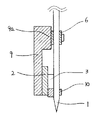
図1は、本発明の走査型プローブ顕微鏡の概略図である。
本発明の走査型プローブ顕微鏡は、先端が探針状に加工されたプローブ1と、 励振用圧電体2と交流電圧発生手段からなる励振部と、検出用圧電体3と電流電圧増幅回路からなる振動検出部と、プローブおよび励振用圧電体および検出用圧電体を保持するためのプローブホルダ4と、プローブをサンプルに接近させる粗動 機構8と、Z軸微動素子7aとZサーボ回路からなるサンプルとプローブ間の距離 制御手段と、XY微動素子7bとXY走査回路からなる2次元走査手段と、測定信号の3次元画像化を行うデータ処理装置とから構成される。
【0013】
検出用圧電体3は、励振用圧電体2とともにプローブホルダ4に取り付けられる 。一方、プローブ1は検出用圧電体とは独立にプローブホルダ4に固定され、先端付近が検出用圧電体3に押し当て固定される。このとき、プローブ自体を撓ませ ることにより、検出用圧電体との接触部3aに押圧が掛かり検出用圧電体上に安定に接合される。
【0014】
検出用圧電体3は、プローブとの接触面積を小さくして、プローブを交換した場合においても取付状態の再現性が保たれ、プローブの振幅やQ値などの振動パ ラメータのばらつきや、力検出における検出特性のばらつきを小さくするために、プローブ1の軸方向と検出用圧電体3の梁の長手方向を概平行に接合する場合に比べて、プローブと検出用圧電体の接合部の接触面積が小さくなるようにプローブ1に対して検出用圧電体3を接合面内で傾けて配置される。
【0015】
また、プローブホルダ上のプローブの固定部4aに傾斜を設け、プローブを撓ませた場合、検出用圧電体との接合部より先端部が、サンプル5に対して垂直とな るように角度と取付位置を規定している。
このようにセットされた、プローブ1を励振用圧電体2により、検出用圧電体3 とともに、サンプル表面と平行に振動させながらサンプル5に接近させると、シ アーフォースがプローブに作用し、プローブの振動振幅が減少する。プローブ1 と検出用圧電体3は接合され一体として動作するため、プローブ1の振動振幅の減少は検出用圧電体3の振幅の減少となる。この振幅の減少は検出用圧電体3の出力電流を減少させる。出力電流は電流電圧増幅回路で検出され、検出用圧電体3の 出力電流の変化量が一定になるように、Z軸微動素子7aとZサーボ回路によりサンプル5とプローブ1間の距離を制御する。このような状態でプローブ1をサンプ ル面上で2次元走査し、サンプルの形状を測定する。この測定信号をもとに、データ処理装置で3次元画像を得るようにした。
【0016】
このとき使用される検出用圧電体3の出力電流は、プローブ1と接合された1本の振動体のみから発生する。このように1本の振動体からなる検出用圧電体を用いることで、フォーク型水晶振動子を用いる走査型プローブ顕微鏡のようにプローブと接合されていない振動片の影響による誤動作がなく、サンプルから受ける力を直接反映した出力信号が得られ、プローブとサンプルの距離を正確に制御する走査型プローブ顕微鏡が実現可能である。
【0017】
【実施例】
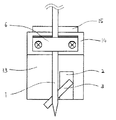
図1に本発明の走査型プローブ顕微鏡の第1の実施例の概略図を示す。また、図1のプローブホルダ部の正面図を図2に、図2の右側面図を図3に示す。
本実施例では、走査型プローブ顕微鏡の一種である走査型近接場顕微鏡に使用される光ファイバーの先端を探針状に加工したストレート型のプローブを使用した。
【0018】
検出用圧電体として、幅0.25mmラ厚さ0.1mmで、長さが5mmの水晶を材料とする梁を使用し、励振用圧電体には、縦10mmラ横5mmラ厚さ0.5mmの平板状に加工したPZTを使用した。励振用圧電体2はホルダ本体4に接着固定され、更に検出用圧電体3は励振用圧電体2に接着固定される。なお、励振用圧電体2と検出用圧電体3は電気的に絶縁されている。
【0019】
プローブ1はプローブ保持用治具6に固定され、治具ごとホルダ本体にネジ止め固定される。
検出用圧電体3はプローブ1の軸方向と、検出用圧電体3の梁の長手方向を一致 させて接合する場合に比べて接合部の面積が小さくなるように、プローブ1の軸 に対して、45度程度傾けられ、プローブ1を保持用治具6により固定部に固定した場合にプローブ1の先端部と検出用圧電体3が交差するよう配置した。なお、プローブ1と検出用圧電体3の接触面内での角度はプローブ1の軸方向と、検出用圧電 体3の長手方向を概平行状態で接合する場合に比べて接合部の面積が小さくなる ような状態であれば任意に設定できる。
【0020】
ホルダの固定部4aはプローブ1と検出用圧電体3が接合したときにプローブに撓みが生じ接合部に押し圧がかかるように、傾斜が設けられている。このとき、接合部より先端の部分がサンプル5に対して垂直となるように、取付部の高さと傾 斜角があらかじめ規定されている。
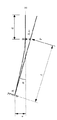
ここで、図11の模式図を用いて、プローブの取付方法と押圧の関係を説明する。
【0021】
図11に示すように、プローブと検出用圧電体の接触点をBとし、Bを通り、サンプルに対して垂直となる方向にZ軸をとる。プローブをZ軸から高さaだけ離れた 位置に角度αで固定する。ここで、A点はプローブの固定端である。
ここで、固定端Aから長さlの部分をΔωだけ撓ませて、B点において接触させ た場合、B点に掛かる押圧Pは式(1)となる。
【0022】
P=2EIα/l2 (1)
ここで、Eはプローブの材質のヤング率、Iはプローブの中立軸に関する断面二次モーメントである。
また、aとαの関係はαが微小な場合、式(2)となる。
a=lα/3 (2)
本実施例では、プローブの材料を石英ガラス製の光ファイバーとした。光ファイバーのヤング率Eと直径dをそれぞれ、E=6.9×10¹⁰Pa、直径d=125×10-6mとする。ここで、 長さlをl=14.5×10⁻³mに設定し、式(1)、式(2)より、a、α、Pをそれぞれ、a=8 ×10⁻⁴m、α=0.17 rad(9.5deg)、P=1.30mNに設定した。
【0023】
ここで、押圧Pが小さすぎた場合には、励振したときに、プローブと検出用圧 電体が離れてしまい動作が不安定になる。またPが大きすぎる場合には、励振力 が抑制されてしまい、やはり動作が不安定になるため前記の式に従って、実験により最適化した。また、接合部からプローブ先端までの長さdは任意に設定可能 であるが、dが著しく長くなると応答性が悪くなりやはり動作が不安定になるた め、本実施例ではd=1mmとした。
【0024】
以上のように構成することにより、固定に接着を用いないため、温度などの環境変化による固定部の状態変化を防ぐことができ、また接着剤の量や接着方法による固定状態のばらつきを押さえることが可能となった。その結果、プローブの振幅やQ値などの振動パラメータの変化や、力検出における検出特性の変化を防 止できた。特に、温度変化の影響を受けないため、極低温下や高温下での測定に有効である。
【0025】
また、検出用圧電体は繰り返し使用が可能である。
さらに、サンプルに対してプローブ先端が垂直でない場合には走査型近接場顕微鏡の光学像やシアフォースを利用した表面形状の分解能が低下するが、サンプルに対してプローブが垂直に設置されるため、分解能の低下が防止される。
本実施例では弾性体のバネ圧のみで接合を行ったが、外乱によるずれを防止するため、バネ圧に加えて補助的に接着剤で接合することも考えられる。接着力の弱いものを用いれば、接合状態はバネ圧に依存するため、接着剤に影響は少ない。さらに、接着力を弱くすれば、検出用圧電体から取り外しも可能となり繰り返し使用も可能である。
【0026】
このように構成したプローブホルダを使用して、励振用圧電体2に交流電圧を 印加すると、励振用圧電体2が振動し、検出用圧電体3が励振される。励振の周波数を検出用圧電体3の共振周波数にすると、検出用圧電体3が共振する。検出用圧電体3が振動すると、圧電効果により検出用圧電体3の電極に電荷が誘起され、電流として電流電圧増幅回路により検出される。検出用圧電体の振動振幅に比例した電流が発生するため、検出された電流により検出用圧電体の振動状態が測定できる。
【0027】
プローブホルダの下側には、XYZ微動素子7が配置され、微動素子上にサンプル5が載置される。微動素子としては、XYZの3軸スキャナーが一体となった円筒形ピエゾ圧電素子を用いた。微動素子としては、この他、Z軸とXY軸が分離したピエゾスキャナーや電歪素子を用いたものが考えられ、本発明に含まれる。この他、ピエゾステージや平行バネを用いたステージ、1軸ピエゾ素子をXYZの3軸に 配置し一体化したトライポッド形圧電素子、積層形のピエゾスキャナーなどが考えられ、いずれも本発明に含まれる。
【0028】
XYZ微動素子上のサンプル5は粗動機構8を用いてプローブ1に接近させる。粗動機構としては、ステッピングモーターと減速ギヤ、粗動ネジからなる粗動機構を用いた。粗動機構としては、この他にZステージにステッピングモーターを付加したものや、圧電素子を用いたステージ、例えばインチワーム機構などやZステージと圧電素子を組み合わせたステージなどが考えられ、いずれも本発明に含まれる。
【0029】
XY走査回路とZサーボ回路のデータはデータ処理装置へ入力され、3次元画像 化される。データ処理手段としては、電子計算機とCRT表示体を用いた。データ処理手段としてはこの他、ストレージオシロスコープや電子計算機と液晶表示体の組み合わせなど種々の方法が考えられるが、いずれも本発明に含まれる。
図4は、本発明の走査型プローブ顕微鏡の第2の実施例のプローブホルダ部の正面図、図5は図4のA-A線断面図である。
【0030】
本実施例では、図2の実施例と同様に、光ファイバーの先端を探針状に加工し たストレート型のプローブを使用し、また、検出用圧電体として、幅0.25mm×厚さ0.1mmで、長さが5mmの水晶を材料とする梁を使用し、励振用圧電体には、縦10mm×横5mm×厚さ0.5mmの平板状に加工したPZTを使用した。励振用圧電体2はホルダ本体に接着固定され、更に検出用圧電体3は励振用圧電体2に接着固定される。なお、励振用圧電体2と検出用圧電体3は電気的に絶縁されている。
【0031】
プローブ1はプローブ保持用治具6に固定され、治具ごとホルダ本体の取付部9aにネジ止め固定される。
検出用圧電体3はプローブ1の軸方向と、検出用圧電体3の梁の長手方向を一致 させて接合する場合に比べて接合部の面積が小さくなるように、プローブ1の軸 に対して、45度程度傾けられ、プローブ1を保持用治具6により固定部9aに固定した場合にプローブ1の先端部と検出用圧電体3が交差するように配置される。
【0032】
プローブの接合は、検出用圧電体3とプローブ1を交差させ、プローブの上から板バネ10の弾性を利用して押し付けるような方法を用いた。
本実施例の場合にも、固定に接着を用いないため、温度などの環境変化による固定部の状態変化を防ぐことができ、また接着剤の量や接着方法による固定状態のばらつきを押さえることが可能となった。その結果、プローブの振幅やQ値な どの振動パラメータの変化や、力検出における検出特性の変化を防止できた。また、検出用圧電体は繰り返し使用が可能である。
【0033】
接合に用いる弾性体としては板バネの他、コイル状のバネやゴムなどが考えられ、いずれも本発明に含まれる。
図6に本発明の走査型プローブ顕微鏡の第3の実施例のプローブホルダ部の正面図を、図7に図6の右側面図を示す。
本実施例でも、先の実施例と同様に、光ファイバーの先端を探針状に加工したストレート型のプローブを使用し、また、検出用圧電体として、棒状に加工した水晶を使用し、励振用圧電体には、平板状に加工したPZTを使用した。励振用圧 電体2はホルダ本体に接着固定され、更に検出用圧電体3は励振用圧電体2に接着 固定される。なお、励振用圧電体2と検出用圧電体3は電気的に絶縁されている。
【0034】
プローブ1はプローブ保持用治具6に固定され、治具ごとホルダ本体の取付部11aにネジ止め固定される。
検出用圧電体3はプローブ1の軸方向と、検出用圧電体3の梁の長手方向を一致 させて接合する場合に比べて接合部の面積が小さくなるように、プローブの軸に対して、45度程度傾けられ、プローブ1を保持用治具6により固定部11aに固定し た場合にプローブ1の先端部と検出用圧電体3が交差するよう配置される。
【0035】
プローブの接合は、検出用圧電体3とプローブ1を交差させ、接合部12を接着により行う方式とした。本実施例の場合、先の実施例とは異なり、検出用圧電体3の再利用が困難になったり、接着接合のため、温度などの環境変化を受けやすく、また、接合部12の接着状態のばらつきが多くなってしまうが、プローブの軸方向と検出用圧電体の梁の長手方向を概平行に接着固定する従来技術に比べ、検出用圧電体を接合面内で斜めに配置した効果により、接合部の面積が小さくなり、そのため、接合状態のばらつきが少なくなる。
【0036】
図8に本発明の走査型プローブ顕微鏡の第4の実施例のプローブホルダ部の正面図を、図9に図8右側面図を示す。本実施例は、基本的に図2と同様の装置構成で、同じ原理によりプローブ1と検出用圧電体3が接合されるが、プローブの取付角度を微調整できる機構を取り付けた。プローブ取付用の治具固定部14がホルダ本体13に枢着され、固定部14とホルダ本体13の間にくさび型の部材15を入れる。くさび型部材15を送りネジ機構(図示せず)で挿入することにより、プローブの取付角度が可変となり、サンプルに対するプローブ先端の角度の微調が可能となる。
【0037】
以上、説明した第1から第4の実施例において、励振用圧電体としては、板状PZTの他、円筒形のPZTスキャナーや積層PZT板などが考えられ、いずれも本発明に含まれる。
また、検出用圧電体の材料としては水晶のほか、PZTなどの圧電性を有するほ かの材料で形成された圧電体も本発明に含まれる。また、形状も断面が長方形の梁に限らず、断面が三角形や丸形のものなど任意の断面を有する梁や、フォーク型水晶振動子、バイモルフ型圧電素子、弾性部材に圧電薄膜を貼り付けた任意形状の検出装置なども考えられ、いずれも本発明に含まれる。さらに、検出用圧電体と励振用圧電体を一体化することも考えられる。
【0038】
また、図12に示すように、検出用圧電体にコストの安い時計用のフォーク型水晶振動子16を検出用圧電体に流用し、フォーク型水晶振動子の片側の振動片16bを欠き、1本の振動片16aのみの振動体に加工して用いることも考えられる。
従来のフォーク型水晶振動子を用いた方法では、プローブと接合している振動片16aは、プローブを介してサンプルからの力を受け振動振幅が減少するが、他 方の振動片16bは元の振動状態を維持し、2本の振動片の振動状態は全く異なり 、一方は力を検出して変化するが他方は変化しないため、合成した出力は、直接に力を反映したものにはならなかった。
【0039】
図12に示すように時計用水晶振動子を加工して検出用圧電体に用いることにより、プローブと接合されていない振動片16bが検出信号に影響を及ぼし誤動作 することが防止される。したがって、フォーク形水晶振動子の出力をZサーボのフィードバック信号として使用した場合、プローブとサンプルの距離を正確に制御できないという欠点が改善され、安定した出力特性を有しサンプルから受ける力を直接反映した出力信号を出す水晶振動子を得ることが可能となる。この結果、プローブとサンプルの距離を正確に制御でき、安定した装置特性により測定データの再現性を高めることが可能となった。
【0040】
また、プローブとしては、ストレート型の光ファイバープローブのほかにも、棒状のタングステンの先端を化学エッチングし、テーパー状に加工した金属製プローブや、ガラスピペットをテーパー状に加工したもの、光ファイバーの先端を曲げたベント型のプローブも本発明に含まれる。さらには第2、第3の実施例ではシリコンや窒化シリコンのカンチレバーを弾性体のバネ圧で接合したり、接着接合で使用する方法も考えられる。ストレート型プローブではシアフォースで制御を行ったが、ベント型のプローブやカンチレバーの場合には、原子間力により制御を行う。先端の加工方法については、化学エッチングや機械的研磨、加熱延伸加工も考えられ、いずれも本発明に含まれる。さらに探針先端については、磁性膜を形成し磁気力検知プローブとしたものや、金または白金膜を形成し、導電性プローブとしたものも考えられ、いずれも本発明に含まれる。
【0041】
【発明の効果】
以上説明したように、本発明の走査型プローブ顕微鏡では、
(1)先端が探針状に加工されたプローブと、励振用圧電体と交流電圧発生手段からなる励振部と、検出用圧電体と電流電圧増幅回路からなる振動検出部と、プローブおよび励振用圧電体および検出用圧電体を保持するためのプローブホルダと、プローブをサンプルに接近させる粗動機構と、Z軸微動素子とZサーボ回路からなるサンプルとプローブ間の距離制御手段と、XY微動素子とXY走査回路からなる2次元走査手段と、測定信号の3次元画像化を行うデータ処理手段とからなる走査型プローブ顕微鏡において、プローブと検出用圧電体の接合を板バネなどの弾性体のバネ圧やプローブ自体の弾性を利用して行うようにした。
【0042】
このようなプローブと検出用圧電体の接合方法を用いることにより、固定に接着を用いないため、温度などの環境変化による固定部の状態変化を防ぐことができ、また接着剤の量や接着方法による固定状態のばらつきを押さえることが可能となる。その結果、プローブの振幅やQ値などの振動パラメータの変化や、力検 出における検出特性の変化を防止できる。
【0043】
また、検出用圧電体の再利用が可能となり、プローブの組立工程が短縮され、検出用圧電体にかかるコストも削減できる。
さらに、プローブ自体の弾性を利用して、プローブと検出用圧電体との接合を行う場合、プローブの先端がサンプル面に対して垂直になるようにプローブと検出用圧電体との取付角度を規定した取付部をプローブホルダに設けた。
【0044】
この方法により、プローブの先端がサンプル面に対して垂直になり、分解能の低下なしに測定を行うことが可能となる。
さらに、本発明では、プローブの軸方向と検出用圧電体の梁の長手方向を概平行に接合する場合に比べて、プローブと検出用圧電体の接合部の接触面積が小さくなるようにプローブに対して検出用圧電体を接合面内で傾けて配置した。
【0045】
この方法により、長手方向に一様に接合する場合に比べて、プローブと検出用圧電体との接触面積が小さくなり、プローブを交換した場合においても取付状態の再現性が向上し、プローブの振幅やQ値などの振動パラメータのばらつきや、 力検出における検出特性のばらつきが小さくなった。その結果、安定した制御を行うことが可能となった。
【0046】
さらに、1本の振動体を有する圧電体により検出用圧電体を構成した。
この結果、サンプルから受ける力を直接反映した出力信号を出す検出用圧電体が得られ、プローブとサンプルの距離を正確に制御することが可能となった。
【図面の簡単な説明】
【図1】本発明走査型プローブ顕微鏡の第1の実施例の概略図である。
【図2】図1の実施例に示したプローブホルダ部の正面図である。
【図3】図2の右側面図である
【図4】本発明の走査型プローブ顕微鏡の第2の実施例のプローブホルダ部の正面図である。
【図5】図4のA-A線断面図である。
【図6】本発明の走査型プローブ顕微鏡の第3の実施例のプローブホルダ部の正面図で ある。
【図7】図6の右側面図である。
【図8】本発明の走査型プローブ顕微鏡の第4の実施例のプローブホルダ部の正面図で ある。
【図9】図8の右側面図である。
【図10】従来のフォーク型水晶振動子を用いる走査型プローブ顕微鏡の概略図である。
【図11】プローブの取付方法を説明するための模式図である。
【図12】フォーク型水晶振動子の片側の振動片を欠き、1本の振動片のみを検出用圧電体に用いた場合の概略図である。
【符号の説明】
1 プローブ
2 励振用圧電体
3 検出用圧電体
4 プローブホルダ
5 サンプル
6 プローブ保持用治具
7 XYZ微動素子
8 粗動機構
9 プローブホルダ
10 板バネ
11 プローブホルダ
12 接着部
13 プローブホルダ
14 治具固定部
15 くさび型部材
16 フォーク型水晶振動子[0001]
BACKGROUND OF THE INVENTION
The present invention relates to a scanning probe microscope using a piezoelectric body as a probe distance control means.
[0002]
[Prior art]
Conventionally, as a scanning probe microscope using a piezoelectric body as a probe distance control means, for example, a scanning probe microscope using a fork type quartz vibrator has been known. For example, according to Kared Karai et al., Appl. Phys. Lett. 66 (14), 1995, pages 1842 to 1844 and JP-A-9-89911, a scanning probe microscope using such a fork type crystal resonator Is disclosed. FIG. 10 is a schematic view of a main part of a scanning probe microscope using a fork type crystal resonator. 400 is an optical fiber probe, and 410 is a fork type crystal resonator. An optical fiber probe is bonded to a crystal resonator, and the crystal resonator is excited by an excitation piezoelectric body (not shown in FIG. 10). When excited, the quartz oscillator generates a current due to the piezoelectric effect. By detecting this current, the vibration state of the crystal resonator can be measured. When the probe approaches the sample, a horizontal force from the sample, that is, a shear force acts on the probe, and the vibration state of the crystal unit bonded to the probe changes. Use a Z-axis fine movement element (not shown in Fig. 10) to keep the shear force constant, that is, to keep the change in the amplitude or phase of the crystal oscillator output constant. Adjust.
[0003]
[Problems to be solved by the invention]
However, the scanning probe microscope using such a conventional fork type crystal resonator has the following problems.
(1) Since the probe is bonded and fixed to the fork type crystal resonator, the fixed state greatly changes due to environmental changes such as temperature. In addition, it is difficult to keep the fixed portion constant depending on the amount of adhesive and the bonding method. As a result, vibration parameters such as probe amplitude and Q value change, and detection characteristics in force detection change, resulting in unstable control.
[0004]
(2) It is difficult to reuse the fork-type quartz resonator because of adhesive fixation.
(3) Since the longitudinal direction of one side surface of the fork type crystal resonator and the axial direction of the probe are fixed in parallel, the contact area between the probe and the resonator is increased. When the contact area increases, the reproducibility of the mounting state becomes difficult, and the variation in detection parameters for vibration parameters such as probe amplitude and Q value and force detection increases.
[0005]
(4) In a fork-type crystal resonator, a vibrating piece that is not bonded to the probe may affect the detection signal and malfunction. That is, in the case of a fork-type crystal resonator, the vibration piece bonded to the probe receives a force from the sample through the probe and the vibration amplitude decreases, but the other vibration piece maintains the original vibration state. As described above, the vibration states of the two vibrating bars are completely different, and one of them changes by detecting a force but the other does not change. Therefore, the synthesized output does not directly reflect the force. When this output is used as a feedback signal for the Z servo, there is a drawback that the distance between the probe and the sample cannot be accurately controlled.
[0006]
Therefore, the present invention has the following problems.
(1) Provided is a scanning probe microscope which can maintain a fixed vibration state and stable vibration characteristics and detection characteristics regardless of environmental changes such as temperature, the amount of adhesive and the bonding method.
(2) Piezoelectric detectionbodyA scanning probe microscope that can be reused is provided.
(3) Detection piezoelectricity that reduces variations in vibration parameters such as probe amplitude and Q value, and variations in detection characteristics in force detectionbodyAnd provide a method of fixing the probe.
(4) Piezoelectric detector for detection that outputs an output signal that directly reflects the force received from the samplebodyThus, a scanning probe microscope that accurately controls the distance between the probe and the sample is provided.
[0007]
[Means for Solving the Problems]
In order to solve the above-described problems, the scanning probe microscope of the present invention has a configuration as described below.
(1) A probe whose tip is processed into a probe shape, an excitation unit composed of an excitation piezoelectric body and AC voltage generating means, a vibration detection unit composed of a detection piezoelectric body and a current-voltage amplification circuit, a probe, and an excitation A probe holder for holding the piezoelectric body and the detection piezoelectric body, a coarse movement mechanism for causing the probe to approach the sample, a distance control means between the sample and the probe comprising a Z-axis fine movement element and a Z servo circuit, and an XY fine movement element In a scanning probe microscope comprising a two-dimensional scanning means comprising an XY scanning circuit and a data processing device for producing a three-dimensional image of a measurement signal, the probe and the detection piezoelectric member are joined by a spring pressure of an elastic body. I made it.
[0008]
This method eliminates the need for an adhesive to join the probe and the detection piezoelectric member, and allows stable vibration characteristics and detection characteristics to be obtained without being affected by the adhesive.bodyCan be reused.
(2) The elasticity of the probe itself is used to join the probe and the detection piezoelectric member. In this case, the probe holder is provided with an attachment portion that defines an attachment angle between the probe and the detection piezoelectric body so that the tip of the probe is perpendicular to the sample surface.
[0009]
This method eliminates the need for an adhesive to join the probe and the detection piezoelectric member, and also attaches the probe and the detection piezoelectric member so that the tip of the probe is perpendicular to the sample surface.ButSince the adjustment is performed, a decrease in resolution is also prevented.
(3) Compared with the case where the axial direction of the probe and the longitudinal direction of the beam of the piezoelectric body for detection are joined approximately in parallel,Piezoelectric body for detectionTo the probe so that the contact area of the joint of thePiezoelectric body for detectionWere placed in a tilted manner in the joint surface.
[0010]
This method reduces the contact area between the probe and the piezoelectric detector for detection compared with the case where the probe is uniformly bonded in the longitudinal direction, improves the reproducibility of the mounting state even when the probe is replaced, and increases the amplitude of the probe. Variations in vibration parameters such as and Q values and variations in detection characteristics in force detection are reduced.
(4) The detecting piezoelectric member is constituted by a piezoelectric beam having one vibrating member.
[0011]
With this method, a detection piezoelectric sensor that outputs an output signal that directly reflects the force received from the sample.bodyAnd the distance between the probe and the sample can be accurately controlled.
[0012]
DETAILED DESCRIPTION OF THE INVENTION
FIG. 1 is a schematic view of a scanning probe microscope of the present invention.
The scanning probe microscope of the present invention comprises a
[0013]
The detection
[0014]
The piezoelectric body for
[0015]
In addition, when the
When the
[0016]
The output current of the detecting
[0017]
【Example】
FIG. 1 shows a schematic diagram of a first embodiment of the scanning probe microscope of the present invention. 1 is a front view of the probe holder portion of FIG. 1, and FIG. 3 is a right side view of FIG.
In this embodiment, a straight type probe in which the tip of an optical fiber used in a scanning near-field microscope, which is a kind of scanning probe microscope, is processed into a probe shape is used.
[0018]
Piezoelectric for detectionbodyUsing a beam made of quartz with a width of 0.25 mm, a thickness of 0.1 mm, and a length of 5 mm, the excitation piezoelectric body was processed into a flat plate with a length of 10 mm, a width of 5 mm, and a thickness of 0.5 mm. PZT was used. The
[0019]
The
The
[0020]
The
Here, the relationship between the probe mounting method and the pressing will be described with reference to the schematic diagram of FIG.
[0021]
As shown in FIG. 11, the contact point between the probe and the detection piezoelectric member is B, and the Z-axis is taken in a direction passing through B and perpendicular to the sample. Fix the probe at an angle α at a position a height a away from the Z axis. Here, point A is the fixed end of the probe.
Here, when the portion of the length l from the fixed end A is bent by Δω and brought into contact at the point B, the pressure P applied to the point B is expressed by the equation (1).
[0022]
P = 2EIα / l2 (1)
Here, E is the Young's modulus of the material of the probe, and I is the second moment of section with respect to the neutral axis of the probe.
Further, the relationship between a and α is expressed by Equation (2) when α is very small.
a = lα / 3 (2)
In this embodiment, the probe material is an optical fiber made of quartz glass. The Young's modulus E and the diameter d of the optical fiber are E = 6.9 × 10¹⁰ Pa and the diameter d = 125 × 10 respectively.-6m. Where the length l is l = 14.5 × 10⁻³m, and from Equation (1) and Equation (2), a, α, and P are each a = 8 × 10-Fourm, α = 0.17 rad (9.5 deg), and P = 1.30 mN were set.
[0023]
Here, when the pressure P is too small, the probe becomes separated from the detection piezoelectric body when excited, and the operation becomes unstable. In addition, when P is too large, the excitation force is suppressed, and the operation becomes unstable. Therefore, the experiment was optimized according to the above equation. In addition, the length d from the joint to the probe tip can be set arbitrarily. However, if d is significantly long, the response will deteriorate and the operation will be unstable. .
[0024]
By configuring as described above, since bonding is not used, it is possible to prevent changes in the state of the fixing portion due to environmental changes such as temperature, and to suppress variations in the fixing state due to the amount of adhesive and the bonding method. Became possible. As a result, it was possible to prevent changes in vibration parameters such as probe amplitude and Q value, as well as changes in detection characteristics in force detection. In particular, since it is not affected by temperature changes, it is effective for measurement at extremely low or high temperatures.
[0025]
Further, the detection piezoelectric body can be used repeatedly.
Furthermore, when the probe tip is not perpendicular to the sample, the resolution of the surface shape using the optical image and shear force of the scanning near-field microscope decreases, but the probe is placed perpendicular to the sample, A reduction in resolution is prevented.
In this embodiment, the joining is performed only with the spring pressure of the elastic body. However, in order to prevent the displacement due to the disturbance, it is conceivable to join with an adhesive in addition to the spring pressure. If a material having a weak adhesive force is used, the bonding state depends on the spring pressure, so that the adhesive has little influence. Further, if the adhesive force is weakened, it can be detached from the detection piezoelectric body and can be used repeatedly.
[0026]
When an AC voltage is applied to the
[0027]
The XYZ
[0028]
The
[0029]
The data of the XY scanning circuit and Z servo circuit are input to the data processing device and converted into a three-dimensional image. As a data processing means, an electronic computer and a CRT display were used. In addition to this, various methods such as a combination of a storage oscilloscope, an electronic computer, and a liquid crystal display can be considered as the data processing means, all of which are included in the present invention.
FIG. 4 is a front view of the probe holder portion of the second embodiment of the scanning probe microscope of the present invention, and FIG. 5 is a cross-sectional view taken along line AA in FIG.
[0030]
In this example, as in the example of FIG. 2, a straight type probe in which the tip of an optical fiber was processed into a probe shape was used, and a piezoelectric body for detection had a width of 0.25 mm × thickness of 0.1 mm. A beam made of quartz with a length of 5 mm was used, and PZT processed into a flat plate of 10 mm length × 5 mm width × 0.5 mm thickness was used as the excitation piezoelectric body. The
[0031]
The
The
[0032]
The probe was joined by using a method in which the
Even in the case of this embodiment, since no bonding is used for fixing, it is possible to prevent a change in the state of the fixing portion due to an environmental change such as temperature, and to suppress variations in the fixing state due to the amount of adhesive or the bonding method. It has become possible. As a result, it was possible to prevent changes in vibration parameters such as probe amplitude and Q value and changes in detection characteristics during force detection. Further, the detection piezoelectric body can be used repeatedly.
[0033]
As the elastic body used for bonding, a plate spring, a coiled spring, rubber or the like can be considered, and any of them is included in the present invention.
FIG. 6 is a front view of the probe holder portion of the third embodiment of the scanning probe microscope of the present invention, and FIG. 7 is a right side view of FIG.
Also in this embodiment, as in the previous embodiment, a straight type probe in which the tip of an optical fiber is processed into a probe shape is used, and a quartz crystal processed into a rod shape is used as a piezoelectric body for detection. PZT processed into a flat plate shape was used as the piezoelectric body. The
[0034]
The
With respect to the probe axis, the
[0035]
The probe was joined by crossing the
[0036]
FIG. 8 is a front view of the probe holder portion of the fourth embodiment of the scanning probe microscope of the present invention, and FIG. 9 is a right side view of FIG. In this example, the apparatus configuration is basically the same as that shown in FIG. 2, and the
[0037]
As described above, in the first to fourth embodiments described above, a piezoelectric PZT, a cylindrical PZT scanner, a laminated PZT plate, and the like can be considered as the excitation piezoelectric body, and these are included in the present invention.
In addition to quartz, the piezoelectric material for detection includes a piezoelectric material formed of other materials having piezoelectricity such as PZT. Also, the shape is not limited to a beam having a rectangular cross section, and a piezoelectric thin film is attached to a beam having an arbitrary cross section such as a triangular or round cross section, a fork type crystal resonator, a bimorph type piezoelectric element, or an elastic member. Arbitrary-shaped detection devices and the like are also conceivable and any of them is included in the present invention. It is also conceivable to integrate the detection piezoelectric member and the excitation piezoelectric member.
[0038]
Further, as shown in FIG. 12, a low-cost fork type
In the conventional method using a fork-type crystal resonator, the vibration piece 16a joined to the probe receives a force from the sample via the probe, and the vibration amplitude decreases, while the other vibration piece 16b has the original vibration piece 16b. The vibration state is maintained, and the vibration states of the two vibrating pieces are completely different. One of them changes by detecting force but the other does not change, so the synthesized output does not directly reflect the force. It was.
[0039]
As shown in FIG. 12, by processing a quartz crystal for a watch and using it as a piezoelectric body for detection, it is possible to prevent the vibration piece 16b not joined to the probe from affecting the detection signal and malfunctioning. Therefore, when using the output of a fork-type crystal unit as a feedback signal for the Z servo, the disadvantage of not being able to accurately control the distance between the probe and the sample has been improved, and it has a stable output characteristic and directly reflects the force received from the sample. It is possible to obtain a crystal resonator that outputs the output signal. As a result, the distance between the probe and the sample can be accurately controlled, and the reproducibility of the measurement data can be improved with stable device characteristics.
[0040]
In addition to straight-type optical fiber probes, the probe can be a metal probe that has been chemically etched at the tip of a rod-like tungsten and processed into a tapered shape, a glass pipette that has been processed into a tapered shape, or the tip of an optical fiber. A bent bent probe is also included in the present invention. Furthermore, in the second and third embodiments, a method in which a silicon or silicon nitride cantilever is joined by the spring pressure of an elastic body or by adhesive joining can be considered. The straight type probe is controlled by shear force, but the bent type probe or cantilever is controlled by atomic force. As for the processing method of the tip, chemical etching, mechanical polishing, and heat drawing are also conceivable, and any of them is included in the present invention. Further, regarding the tip of the probe, a magnetic film is formed as a magnetic force detection probe, and a gold or platinum film is formed as a conductive probe, both of which are included in the present invention.
[0041]
【The invention's effect】
As described above, in the scanning probe microscope of the present invention,
(1) A probe whose tip is processed into a probe shape, an excitation unit composed of an excitation piezoelectric body and AC voltage generating means, a vibration detection unit composed of a detection piezoelectric body and a current-voltage amplification circuit, a probe, and an excitation A probe holder for holding the piezoelectric body and the detection piezoelectric body, a coarse movement mechanism for causing the probe to approach the sample, a distance control means between the sample and the probe comprising a Z-axis fine movement element and a Z servo circuit, and an XY fine movement element In a scanning probe microscope comprising a two-dimensional scanning means comprising an XY scanning circuit and a data processing means for performing three-dimensional imaging of a measurement signal, an elastic spring such as a leaf spring is used to join the probe and the detection piezoelectric member. The pressure and the elasticity of the probe itself were used.
[0042]
By using such a bonding method of the probe and the piezoelectric body for detection, since the bonding is not used, it is possible to prevent a change in the state of the fixing portion due to an environmental change such as temperature, and the amount of the adhesive and the bonding method It is possible to suppress the variation in the fixed state due to. As a result, it is possible to prevent changes in vibration parameters such as probe amplitude and Q value, as well as changes in detection characteristics during force detection.
[0043]
In addition, the detection piezoelectric body can be reused, the probe assembly process is shortened, and the cost for the detection piezoelectric body can be reduced.
Furthermore, when joining the probe and the detection piezoelectric body using the elasticity of the probe itself, the mounting angle between the probe and the detection piezoelectric body is specified so that the tip of the probe is perpendicular to the sample surface. The attached portion was provided on the probe holder.
[0044]
With this method, the tip of the probe is perpendicular to the sample surface, and measurement can be performed without a reduction in resolution.
Furthermore, according to the present invention, compared to the case where the axial direction of the probe and the longitudinal direction of the beam of the detection piezoelectric body are joined substantially in parallel, the contact area of the joint between the probe and the detection piezoelectric body is reduced. On the other hand, the piezoelectric body for detection was disposed so as to be inclined in the bonding surface.
[0045]
This method reduces the contact area between the probe and the piezoelectric detector for detection compared with the case where the probe is uniformly bonded in the longitudinal direction, improves the reproducibility of the mounting state even when the probe is replaced, and increases the amplitude of the probe. Variations in vibration parameters such as vibration and Q values and variations in detection characteristics in force detection have been reduced. As a result, stable control can be performed.
[0046]
Further, a detection piezoelectric body is constituted by a piezoelectric body having one vibrating body.
As a result, a detection piezoelectric body that outputs an output signal that directly reflects the force received from the sample is obtained, and the distance between the probe and the sample can be accurately controlled.
[Brief description of the drawings]
FIG. 1 is a schematic view of a first embodiment of a scanning probe microscope of the present invention.
FIG. 2 is a front view of the probe holder portion shown in the embodiment of FIG.
FIG. 3 is a right side view of FIG.
FIG. 4 is a front view of a probe holder portion of a second embodiment of the scanning probe microscope of the present invention.
5 is a cross-sectional view taken along line AA in FIG.
FIG. 6 is a front view of a probe holder portion of a third embodiment of the scanning probe microscope of the present invention.
7 is a right side view of FIG. 6. FIG.
FIG. 8 is a front view of a probe holder portion of a fourth embodiment of the scanning probe microscope of the present invention.
9 is a right side view of FIG.
FIG. 10 is a schematic view of a scanning probe microscope using a conventional fork type crystal resonator.
FIG. 11 is a schematic diagram for explaining a method of attaching a probe.
FIG. 12 is a schematic view in the case where a vibrating piece on one side of a fork-type crystal resonator is omitted and only one vibrating piece is used as a detection piezoelectric body.
[Explanation of symbols]
1 Probe
2 Piezoelectric body for excitation
3 Piezoelectric body for detection
4 Probe holder
5 samples
6 Probe holding jig
7 XYZ fine movement element
8 Coarse motion mechanism
9 Probe holder
10 leaf spring
11 Probe holder
12 Bonding part
13 Probe holder
14 Jig fixing part
15 Wedge type member
16 Fork crystal unit
Claims (12)
電圧を印加することで振動する励振用圧電体と、
振動状態を測定するための検出用圧電体と、
前記励振用圧電体と前記検出用圧電体を保持するプローブホルダと、
前記プローブをサンプルに接近させる粗動機構と、Z軸微動素子とZサーボ回路からなるサンプルと前記プローブ間の距離制御手段と、XY微動素子とXY走査回路からなる2次元走査手段と、測定信号の3次元画像化を行うデータ処理装置とからなる走査型プローブ顕微鏡において、
前記プローブと振動状態を測定するための前記検出用圧電体とは、弾性体のバネ圧で接合したことを特徴とする走査型プローブ顕微鏡。A probe whose tip is processed into a probe shape;
An excitation piezoelectric body that vibrates by applying a voltage;
And detecting piezoelectric element for measuring the vibration state,
A probe holder for holding the excitation piezoelectric member and the detection piezoelectric member;
A coarse movement mechanism for bringing the probe closer to the sample, a sample comprising a Z-axis fine movement element and a Z servo circuit, a distance control means between the probes, a two-dimensional scanning means comprising an XY fine movement element and an XY scanning circuit, and a measurement signal In a scanning probe microscope comprising a data processing device for performing three-dimensional imaging of
A scanning probe microscope characterized in that the probe and the detection piezoelectric body for measuring a vibration state are joined by a spring pressure of an elastic body.
Priority Applications (2)
| Application Number | Priority Date | Filing Date | Title |
|---|---|---|---|
| JP16433399A JP3905254B2 (en) | 1998-06-22 | 1999-06-10 | Scanning probe microscope |
| US09/337,613 US6257053B1 (en) | 1998-06-22 | 1999-06-21 | Scanning probe microscope having piezoelectric member for controlling movement of probe |
Applications Claiming Priority (3)
| Application Number | Priority Date | Filing Date | Title |
|---|---|---|---|
| JP10-174424 | 1998-06-22 | ||
| JP17442498 | 1998-06-22 | ||
| JP16433399A JP3905254B2 (en) | 1998-06-22 | 1999-06-10 | Scanning probe microscope |
Related Child Applications (1)
| Application Number | Title | Priority Date | Filing Date |
|---|---|---|---|
| JP2006014383A Division JP4209891B2 (en) | 1998-06-22 | 2006-01-23 | Scanning probe microscope |
Publications (3)
| Publication Number | Publication Date |
|---|---|
| JP2000081443A JP2000081443A (en) | 2000-03-21 |
| JP2000081443A5 JP2000081443A5 (en) | 2005-05-19 |
| JP3905254B2 true JP3905254B2 (en) | 2007-04-18 |
Family
ID=26489478
Family Applications (1)
| Application Number | Title | Priority Date | Filing Date |
|---|---|---|---|
| JP16433399A Expired - Fee Related JP3905254B2 (en) | 1998-06-22 | 1999-06-10 | Scanning probe microscope |
Country Status (2)
| Country | Link |
|---|---|
| US (1) | US6257053B1 (en) |
| JP (1) | JP3905254B2 (en) |
Families Citing this family (20)
| Publication number | Priority date | Publication date | Assignee | Title |
|---|---|---|---|---|
| US6100523A (en) * | 1997-10-29 | 2000-08-08 | International Business Machines Corporation | Micro goniometer for scanning microscopy |
| US6459088B1 (en) * | 1998-01-16 | 2002-10-01 | Canon Kabushiki Kaisha | Drive stage and scanning probe microscope and information recording/reproducing apparatus using the same |
| JP3387846B2 (en) * | 1999-03-04 | 2003-03-17 | セイコーインスツルメンツ株式会社 | Scanning probe microscope |
| US6477898B1 (en) * | 2000-07-06 | 2002-11-12 | Motorola, Inc. | Membrane mask stress measurement apparatus and method therefor |
| US6888135B2 (en) * | 2000-10-18 | 2005-05-03 | Nec Corporation | Scanning probe microscope with probe formed by single conductive material |
| US6748795B1 (en) | 2001-07-27 | 2004-06-15 | Molecular Imaging Corporation | Pendulum scanner for scanning probe microscope |
| JP4782953B2 (en) * | 2001-08-06 | 2011-09-28 | 東京エレクトロン株式会社 | Probe card characteristic measuring device, probe device, and probe method |
| IL145136A0 (en) * | 2001-08-27 | 2002-06-30 | Multiple plate tip or sample scanning reconfigurable scanning probe microscope with transparent interfacing of far-field optical microscopes | |
| US6953930B2 (en) * | 2001-08-27 | 2005-10-11 | Nippon Telegraph And Telephone Corporation | Conductive transparent probe and probe control apparatus |
| US6677697B2 (en) * | 2001-12-06 | 2004-01-13 | Veeco Instruments Inc. | Force scanning probe microscope |
| US6991948B2 (en) * | 2003-11-05 | 2006-01-31 | Solid State Measurements, Inc. | Method of electrical characterization of a silicon-on-insulator (SOI) wafer |
| US7180662B2 (en) * | 2004-04-12 | 2007-02-20 | Applied Scientific Instrumentation Inc. | Stage assembly and method for optical microscope including Z-axis stage and piezoelectric actuator for rectilinear translation of Z stage |
| DE112006003492T5 (en) * | 2005-12-28 | 2008-10-30 | Karma Technology, Inc., Agoura Hills | Special module with integrated actuator for a scanning probe microscope |
| US8302456B2 (en) | 2006-02-23 | 2012-11-06 | Asylum Research Corporation | Active damping of high speed scanning probe microscope components |
| JP2007309919A (en) * | 2006-04-20 | 2007-11-29 | Hitachi Kenki Fine Tech Co Ltd | Scanning probe microscope |
| JP4378385B2 (en) * | 2006-05-17 | 2009-12-02 | キヤノン株式会社 | Driving stage in scanning probe apparatus, scanning probe apparatus |
| JP4899162B2 (en) * | 2007-07-17 | 2012-03-21 | 独立行政法人産業技術総合研究所 | Scanning probe microscope probe and scanning probe microscope using the same |
| KR101065981B1 (en) * | 2009-05-20 | 2011-09-19 | 인하대학교 산학협력단 | Mechanically-coupled vibrating tuning fork-scanning probe system |
| US9383388B2 (en) | 2014-04-21 | 2016-07-05 | Oxford Instruments Asylum Research, Inc | Automated atomic force microscope and the operation thereof |
| CN105092896B (en) * | 2015-08-03 | 2018-06-29 | 中国科学院合肥物质科学研究院 | The multidimensional piezo-electric motor and can search for scanning probe microscopy that single sweep pipe drives |
Family Cites Families (8)
| Publication number | Priority date | Publication date | Assignee | Title |
|---|---|---|---|---|
| CH643397A5 (en) * | 1979-09-20 | 1984-05-30 | Ibm | GRID TUNNEL MICROSCOPE. |
| DE3610540A1 (en) * | 1986-03-27 | 1987-10-01 | Kernforschungsanlage Juelich | MOTION DEVICE FOR MICROMOVING OBJECTS |
| US4800274A (en) * | 1987-02-02 | 1989-01-24 | The Regents Of The University Of California | High resolution atomic force microscope |
| DE4013742C2 (en) * | 1990-04-28 | 1994-06-30 | Focus Mestechnik Gmbh & Co Kg | Scanning head for a machine for measuring the micro surface contour of workpieces |
| JP2500373B2 (en) * | 1993-11-09 | 1996-05-29 | 工業技術院長 | Atomic force microscope and sample observation method in atomic force microscope |
| US6006594A (en) * | 1994-05-11 | 1999-12-28 | Dr. Khaled Und Dr. Miles Haines Gesellschaft Burgerlichen Rechts | Scanning probe microscope head with signal processing circuit |
| JPH10283972A (en) * | 1997-04-10 | 1998-10-23 | Seiko Instr Inc | Machining, recording, and reproducing device using scanning probe microscope |
| US5900618A (en) * | 1997-08-26 | 1999-05-04 | University Of Maryland | Near-field scanning microwave microscope having a transmission line with an open end |
-
1999
- 1999-06-10 JP JP16433399A patent/JP3905254B2/en not_active Expired - Fee Related
- 1999-06-21 US US09/337,613 patent/US6257053B1/en not_active Expired - Lifetime
Also Published As
| Publication number | Publication date |
|---|---|
| JP2000081443A (en) | 2000-03-21 |
| US6257053B1 (en) | 2001-07-10 |
Similar Documents
| Publication | Publication Date | Title |
|---|---|---|
| JP3905254B2 (en) | Scanning probe microscope | |
| EP0871006B1 (en) | Scanning probe microscope | |
| JP3511361B2 (en) | Scanning probe microscope | |
| US5641896A (en) | Coupled oscillator scanning imager | |
| US6439051B2 (en) | Vibrators, vibratory gyroscopes, devices for measuring a linear acceleration and a method of measuring a turning angular rate | |
| USRE42923E1 (en) | Piezoelectric vibration angular velocity meter and camera using the same | |
| EP0871166B1 (en) | Apparatus for machining, recording, or reproducing, using scanning probe microscope | |
| Akiyama et al. | Symmetrically arranged quartz tuning fork with soft cantilever for intermittent contact mode atomic force microscopy | |
| US6006594A (en) | Scanning probe microscope head with signal processing circuit | |
| JP2000081443A5 (en) | ||
| JP4209891B2 (en) | Scanning probe microscope | |
| US6240771B1 (en) | Device for noncontact intermittent contact scanning of a surface and a process therefore | |
| US7038202B2 (en) | Conductive transparent probe and probe control apparatus | |
| JP3387846B2 (en) | Scanning probe microscope | |
| JP2005106786A (en) | Scanning type probe microscope | |
| JPH06323845A (en) | Thin film force detection probe for scanning force microscope | |
| JP3318085B2 (en) | Cantilever tip holder | |
| JP2005227139A (en) | Cantilever for atomic force microscope | |
| JP2000009624A (en) | Scanning probe microscope | |
| JP3431246B2 (en) | Probe excitation mechanism | |
| JPH0989911A (en) | Compound-oscillator scanning imager | |
| JPH10267950A (en) | Lateral-excitation frictional-force microscope | |
| RU2193769C2 (en) | Method measuring characteristics of surface magnetic field with use of scanning sounding microscope | |
| JPH1123589A (en) | Force detecting device and scanning type probe microscope using it | |
| JPH10267947A (en) | Cantilever excitation apparatus |
Legal Events
| Date | Code | Title | Description |
|---|---|---|---|
| RD01 | Notification of change of attorney |
Free format text: JAPANESE INTERMEDIATE CODE: A7421 Effective date: 20040302 |
|
| A711 | Notification of change in applicant |
Free format text: JAPANESE INTERMEDIATE CODE: A712 Effective date: 20040526 |
|
| A521 | Written amendment |
Free format text: JAPANESE INTERMEDIATE CODE: A523 Effective date: 20040709 |
|
| A621 | Written request for application examination |
Free format text: JAPANESE INTERMEDIATE CODE: A621 Effective date: 20040709 |
|
| A977 | Report on retrieval |
Free format text: JAPANESE INTERMEDIATE CODE: A971007 Effective date: 20050714 |
|
| A131 | Notification of reasons for refusal |
Free format text: JAPANESE INTERMEDIATE CODE: A131 Effective date: 20051122 |
|
| A521 | Written amendment |
Free format text: JAPANESE INTERMEDIATE CODE: A523 Effective date: 20060119 |
|
| A521 | Written amendment |
Free format text: JAPANESE INTERMEDIATE CODE: A523 Effective date: 20060123 |
|
| A131 | Notification of reasons for refusal |
Free format text: JAPANESE INTERMEDIATE CODE: A131 Effective date: 20061017 |
|
| A521 | Written amendment |
Free format text: JAPANESE INTERMEDIATE CODE: A523 Effective date: 20061205 |
|
| TRDD | Decision of grant or rejection written | ||
| A01 | Written decision to grant a patent or to grant a registration (utility model) |
Free format text: JAPANESE INTERMEDIATE CODE: A01 Effective date: 20070109 |
|
| A61 | First payment of annual fees (during grant procedure) |
Free format text: JAPANESE INTERMEDIATE CODE: A61 Effective date: 20070111 |
|
| R150 | Certificate of patent or registration of utility model |
Ref document number: 3905254 Country of ref document: JP Free format text: JAPANESE INTERMEDIATE CODE: R150 Free format text: JAPANESE INTERMEDIATE CODE: R150 |
|
| RD01 | Notification of change of attorney |
Free format text: JAPANESE INTERMEDIATE CODE: A7421 Effective date: 20091108 |
|
| FPAY | Renewal fee payment (event date is renewal date of database) |
Free format text: PAYMENT UNTIL: 20110119 Year of fee payment: 4 |
|
| FPAY | Renewal fee payment (event date is renewal date of database) |
Free format text: PAYMENT UNTIL: 20110119 Year of fee payment: 4 |
|
| RD03 | Notification of appointment of power of attorney |
Free format text: JAPANESE INTERMEDIATE CODE: R3D03 |
|
| FPAY | Renewal fee payment (event date is renewal date of database) |
Free format text: PAYMENT UNTIL: 20110119 Year of fee payment: 4 |
|
| FPAY | Renewal fee payment (event date is renewal date of database) |
Free format text: PAYMENT UNTIL: 20120119 Year of fee payment: 5 |
|
| FPAY | Renewal fee payment (event date is renewal date of database) |
Free format text: PAYMENT UNTIL: 20130119 Year of fee payment: 6 |
|
| FPAY | Renewal fee payment (event date is renewal date of database) |
Free format text: PAYMENT UNTIL: 20130119 Year of fee payment: 6 |
|
| R250 | Receipt of annual fees |
Free format text: JAPANESE INTERMEDIATE CODE: R250 |
|
| FPAY | Renewal fee payment (event date is renewal date of database) |
Free format text: PAYMENT UNTIL: 20140119 Year of fee payment: 7 |
|
| S531 | Written request for registration of change of domicile |
Free format text: JAPANESE INTERMEDIATE CODE: R313531 |
|
| S533 | Written request for registration of change of name |
Free format text: JAPANESE INTERMEDIATE CODE: R313533 |
|
| FPAY | Renewal fee payment (event date is renewal date of database) |
Free format text: PAYMENT UNTIL: 20140119 Year of fee payment: 7 |
|
| R350 | Written notification of registration of transfer |
Free format text: JAPANESE INTERMEDIATE CODE: R350 |
|
| R250 | Receipt of annual fees |
Free format text: JAPANESE INTERMEDIATE CODE: R250 |
|
| R250 | Receipt of annual fees |
Free format text: JAPANESE INTERMEDIATE CODE: R250 |
|
| R250 | Receipt of annual fees |
Free format text: JAPANESE INTERMEDIATE CODE: R250 |
|
| R250 | Receipt of annual fees |
Free format text: JAPANESE INTERMEDIATE CODE: R250 |
|
| R250 | Receipt of annual fees |
Free format text: JAPANESE INTERMEDIATE CODE: R250 |
|
| LAPS | Cancellation because of no payment of annual fees |