US6477898B1 - Membrane mask stress measurement apparatus and method therefor - Google Patents
Membrane mask stress measurement apparatus and method therefor Download PDFInfo
- Publication number
- US6477898B1 US6477898B1 US09/610,501 US61050100A US6477898B1 US 6477898 B1 US6477898 B1 US 6477898B1 US 61050100 A US61050100 A US 61050100A US 6477898 B1 US6477898 B1 US 6477898B1
- Authority
- US
- United States
- Prior art keywords
- membrane
- window
- vibration
- frequency
- membrane window
- Prior art date
- Legal status (The legal status is an assumption and is not a legal conclusion. Google has not performed a legal analysis and makes no representation as to the accuracy of the status listed.)
- Expired - Fee Related, expires
Links
Images


Classifications
-
- G—PHYSICS
- G03—PHOTOGRAPHY; CINEMATOGRAPHY; ANALOGOUS TECHNIQUES USING WAVES OTHER THAN OPTICAL WAVES; ELECTROGRAPHY; HOLOGRAPHY
- G03F—PHOTOMECHANICAL PRODUCTION OF TEXTURED OR PATTERNED SURFACES, e.g. FOR PRINTING, FOR PROCESSING OF SEMICONDUCTOR DEVICES; MATERIALS THEREFOR; ORIGINALS THEREFOR; APPARATUS SPECIALLY ADAPTED THEREFOR
- G03F1/00—Originals for photomechanical production of textured or patterned surfaces, e.g., masks, photo-masks, reticles; Mask blanks or pellicles therefor; Containers specially adapted therefor; Preparation thereof
- G03F1/20—Masks or mask blanks for imaging by charged particle beam [CPB] radiation, e.g. by electron beam; Preparation thereof
-
- G—PHYSICS
- G01—MEASURING; TESTING
- G01N—INVESTIGATING OR ANALYSING MATERIALS BY DETERMINING THEIR CHEMICAL OR PHYSICAL PROPERTIES
- G01N29/00—Investigating or analysing materials by the use of ultrasonic, sonic or infrasonic waves; Visualisation of the interior of objects by transmitting ultrasonic or sonic waves through the object
- G01N29/04—Analysing solids
- G01N29/12—Analysing solids by measuring frequency or resonance of acoustic waves
-
- G—PHYSICS
- G01—MEASURING; TESTING
- G01N—INVESTIGATING OR ANALYSING MATERIALS BY DETERMINING THEIR CHEMICAL OR PHYSICAL PROPERTIES
- G01N29/00—Investigating or analysing materials by the use of ultrasonic, sonic or infrasonic waves; Visualisation of the interior of objects by transmitting ultrasonic or sonic waves through the object
- G01N29/22—Details, e.g. general constructional or apparatus details
- G01N29/24—Probes
- G01N29/2418—Probes using optoacoustic interaction with the material, e.g. laser radiation, photoacoustics
-
- G—PHYSICS
- G01—MEASURING; TESTING
- G01N—INVESTIGATING OR ANALYSING MATERIALS BY DETERMINING THEIR CHEMICAL OR PHYSICAL PROPERTIES
- G01N29/00—Investigating or analysing materials by the use of ultrasonic, sonic or infrasonic waves; Visualisation of the interior of objects by transmitting ultrasonic or sonic waves through the object
- G01N29/34—Generating the ultrasonic, sonic or infrasonic waves, e.g. electronic circuits specially adapted therefor
- G01N29/348—Generating the ultrasonic, sonic or infrasonic waves, e.g. electronic circuits specially adapted therefor with frequency characteristics, e.g. single frequency signals, chirp signals
-
- G—PHYSICS
- G03—PHOTOGRAPHY; CINEMATOGRAPHY; ANALOGOUS TECHNIQUES USING WAVES OTHER THAN OPTICAL WAVES; ELECTROGRAPHY; HOLOGRAPHY
- G03F—PHOTOMECHANICAL PRODUCTION OF TEXTURED OR PATTERNED SURFACES, e.g. FOR PRINTING, FOR PROCESSING OF SEMICONDUCTOR DEVICES; MATERIALS THEREFOR; ORIGINALS THEREFOR; APPARATUS SPECIALLY ADAPTED THEREFOR
- G03F1/00—Originals for photomechanical production of textured or patterned surfaces, e.g., masks, photo-masks, reticles; Mask blanks or pellicles therefor; Containers specially adapted therefor; Preparation thereof
- G03F1/68—Preparation processes not covered by groups G03F1/20 - G03F1/50
- G03F1/82—Auxiliary processes, e.g. cleaning or inspecting
- G03F1/84—Inspecting
-
- G—PHYSICS
- G01—MEASURING; TESTING
- G01N—INVESTIGATING OR ANALYSING MATERIALS BY DETERMINING THEIR CHEMICAL OR PHYSICAL PROPERTIES
- G01N2291/00—Indexing codes associated with group G01N29/00
- G01N2291/02—Indexing codes associated with the analysed material
- G01N2291/023—Solids
- G01N2291/0237—Thin materials, e.g. paper, membranes, thin films
Definitions
- the invention relates generally to integrated circuit manufacturing and more particularly to a membrane mask stress measurement apparatus and method therefor.
- SCALPEL x-ray lithography
- IPL ion beam projection lithography
- EUV extreme ultra-violet
- SCALPEL scattering with angular limited projection in electron-beam lithography
- SCALPEL, IPL and x-ray lithography techniques utilize masks that are formed of attenuating elements overlying thin membranes.
- the membrane thickness of a SCALPEL mask is typically in the range of 100-150 nanometers, whereas for XRL and IPL the membrane thickness is typically in the range of 2-5 microns.
- SCALPEL masks typically include 500 to 1000 thin membrane windows approximately 1 mm ⁇ 12 mm in size on a 200 mm silicon starting substrate.
- XRL and IPL masks consist of one large membrane window on a silicon substrate.
- SCALPEL membrane masks can suffer from distortions created through local stress on the membrane. As such, when various layers that may be included in the membrane mask are deposited, the deposition parameters may vary slightly from the ideal parameter settings such that the stress of one layer may not exactly match the expected stress of another layer. This mismatch may cause undesirable stress levels when composite layer membrane masks are formed where significant stress mismatch exists between various layers included in the composite layer structure.
- the stress associated with a particular membrane mask used in the lithographic operations must be determined to lie within predetermined specification levels. By understanding what the stress level is for the membrane mask, the appropriate process alterations can be made to ensure minimal image placement deviations.
- One technique used for measuring stress of thin films on substrates such as silicon wafers is a bow measurement test that measures the curvature of the substrate by reflecting light off the substrate after film deposition. The curvature of the substrate before and after deposition of the thin films is compared to determine the stress induced by the deposition of the thin films.
- Such techniques work well for films having a thickness on the same order as the thickness of the underlying substrate, such techniques do not work well when the film thickness is orders of magnitude smaller than the substrate thickness. This is because the stress associated with the thick substrate renders the stress added by the thin films insignificant.
- membranes made up of thin films alone may be fabricated for stress testing.
- One technique which utilizes such thin film membranes is bulge testing. In bulge testing, the membrane is suspended between two different pressures. The stress of the membrane can then be measured based on the “bulging” or distortion of the membrane resulting from the pressure differential.
- RFT resonant frequency test
- the RFT technique measures the stress of the free-standing membrane by inducing vibrations within the membrane under test. Such vibration inducement is accomplished in one prior art RFT technique through the use of electrostatic force.
- the electrostatic force is generated by applying a sinusoidal voltage to an underlying conductive chuck structure that drives the overlying membrane as well as physically supporting it.
- the chuck includes an array of complementary driving electrodes that correspond to the locations of membrane widows within the membrane mask. Each driving electrode stimulates a corresponding membrane widow.
- a sensing electrode positioned over the membrane under test measures the voltage change generated between the electrode and the vibrating membrane. This is a capacitance-based measurement.
- the voltage and frequency of the input signal applied to the drive electrodes included in the underlying chuck is manually adjusted while the output is observed on an oscilloscope or similar testing apparatus.
- a peak level which can be determined based on the output signal on the oscilloscope
- a resonant frequency of the membrane under test is determined. The resonant frequency is then used in the following formula to determine the stress (in MPa) within the membrane.
- f r is the resonance frequency of the membrane
- ⁇ is the average film density in g/cm 3
- a and b are the rectangular edge length and width of the membrane widow in centimeters
- m and n are the number of halfwaves in the a and b directions, respectively.
- Membrane vibrations are detected using a capacitive measurement that senses a change in capacitance that results from the changing distance between the sensing electrode and the vibrating membrane. This particular RFT technique suffers from a number of disadvantages that may limit its effectiveness in testing membrane masks.
- RFT measurement techniques based on the capacitive excitation cannot measure the resonance frequency of a membrane that does not have a conductive layer.
- the membrane In order to cause the membrane to vibrate due to electrostatic excitation, the membrane must include a conductive layer such that a ground plane is created to allow for the electrostatic excitation. This may be undesirable in some membrane structures where a conductive layer is not present or needed for lithographic purposes. For example, in one instance a single layer membrane may be measured for its stress level, such that this stress level can be compared with the stress level measured after an additional layer has been added to the initially measured layer.
- Prior art RFT techniques are also limited by the need for a custom chuck that includes the drive electrodes for each substrate size and each pattern of membrane windows included on a mask.
- a different chuck with specifically placed and sized drive electrodes will be required in order to achieve the electrostatic excitation desired.
- higher excitation voltages are typically required. These higher excitation voltages may cause a distortion or shifting of the frequency spectrum around the resonant frequency, which is undesirable.
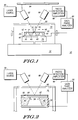
- FIG. 1 includes a graphical representation of a stress measurement apparatus in accordance with a particular embodiment of the present invention
- FIG. 2 includes a magnified view of the membrane under test shown in FIG. 1;
- FIG. 3 illustrates a frequency graph associated with the determination of the resonant frequency of a membrane such that the stress of the membrane can be calculated in accordance with a particular embodiment of the present invention.
- the present invention provides a method and apparatus for determining stress levels of membrane masks that may be used in membrane-based lithographic techniques.
- a piezoelectric plate is used to induce vibrations into the membrane mask, where the gain and phase changes that depend on the frequency of vibrations induced in the membrane mask are optically sensed.
- a frequency graph associated with the membrane mask can be constructed such that resonant frequencies are easily determined. These resonant frequencies can then be used to calculate the stress associated with the membrane mask.
- the piezoelectric plate can provide adequate excitation of the membrane mask using low excitation voltages such that undesirable distortions associated with high excitation voltages are avoided.
- the noise that existed in prior art RFT techniques is also avoided by utilizing optical sensing to measure the vibrations of the membrane mask.
- the optical measurement apparatus associated with measuring the frequency response of each membrane window is easily shifted from one membrane window to the next without having to remove the membrane mask from the vacuum environment.
- the throughput associated with testing membrane masks that include a large number of membrane windows is greatly improved over that of prior art RFT techniques.
- the ease with which the resonant frequency is determined based on the frequency graph provided by the gain phase analyzer simplifies the actual measurement techniques and further improves the expected throughput. Thus, manual interaction with the testing system is minimized, which further increases testing efficiency.
- FIG. 1 illustrates a testing apparatus 10 that includes a piezoelectric plate 30 that excites or stimulates the membrane layer 50 of the mask 35 .
- the mask 35 includes the membrane layer 50 and struts 40 .
- the membrane layer 50 includes a plurality of membrane windows 52 - 56 .
- the excitation of the membrane layer 50 of the mask 35 is measured using an optical sensing unit 90 - 98 .
- the measurements taken by the optical sensing unit 90 - 98 are provided to a gain phase analyzer 80 .
- the gain phase analyzer which may be a Hewlett-Packard 4194A Gain Phase Analyzer, may also provide the excitation to the piezoelectric plate 30 .
- the gain phase analyzer 80 may include a spectrum analyzer and a signal generation circuit. By comparing the input signal provided to the piezoelectric plate 30 with the resulting excitation of the membrane window as detected by optical unit, the frequency response of the membrane window can be determined.
- a station 12 that isolates the rest of the testing apparatus 10 from external vibrations may be included.
- the station 12 which functions as an isolation table, is a vacuum chamber 70 in which a chuck 20 is positioned. Because the chuck 20 does not play an active role in the excitation of the membrane layer 50 , it can be a general purpose chuck and no customization is required to achieve the desired excitation of the membrane layer 50 as was required in prior art techniques that relied on electrostatic excitation.
- a piezoelectric plate 30 is positioned on the chuck 20 .
- the piezoelectric plate 30 may be a piezoelectric film, or other thin layer of piezoelectric material that vibrates in response to applied voltages.
- an electrical signal of varying frequency may be applied to the piezoelectric plate such that acoustic oscillation of varying frequency is applied to the membrane layer 50 .
- the membrane layer 50 is supported by a plurality of struts 40 , where the struts 40 may be positioned in a strut array, which may be referred to as “grillage.”
- the grillage supports the overlying membrane layer 50 , which includes a plurality of membrane windows 52 - 56 .
- the vibrations produced by the piezoelectric plate 30 are transferred through the struts 40 to the membrane layer 50 .
- the amplitude of vibration of the membrane window will increase significantly with respect to the amplitude of vibration in response to frequencies outside of the resonant frequency area.
- the vacuum environment 70 is enclosed by a transparent vacuum cover plate 60 .
- the vacuum cover plate is glass, where the thickness of the glass is sufficient to ensure maintenance of the vacuum environment 70 .
- optical sensing techniques can be utilized to sense the frequency and amplitude of the vibrations of the membrane window 54 shown to be under test in FIG. 1 .
- the frequency and amplitude of the vibrations of the membrane window 54 can be determined based on optical measurement techniques currently known in the art.
- the optical measurement system shown in FIG. 1 includes a laser source 90 that generates a DC light source. This generated laser light is directed toward the membrane window under test using a fiber optic/collimation block 92 that directs and collimates the DC light source. As such, a collimated beam of light is directed at the membrane window 54 that is under test. Measurement of the vibrations of the membrane window under test may be enhanced by directing the beam of light toward the center portion of the membrane window under test. Because the center portion is the portion at which displacement of the membrane window 54 is most pronounced, maximum signal detection can be achieved.
- Reflected light which is actually a beam of light modulated by the membrane vibration, are received and collected by the fiber optic unit 96 .
- the collected portions are provided to the photo detector/amplifier block 98 .
- the photo detector/amplifier block 98 which acts as a light detector, converts the light into electrical signals (which may be referred to as a reflected signal) which are then amplified and provided to the gain phase analyzer 80 .
- the analysis of the reflected signal can determine the frequency response of the vibrations of the membrane window 54 currently under test.
- the fiber optic units 92 and 96 are preferably coupled via a base 94 . As such, repositioning of the base 94 is all that is required to step from one membrane window to the next.
- the gain phase analyzer 80 receives the electrical signals from the photo detector/amplifier 98 .
- the gain phase analyzer 80 may also be the circuit that supplies the excitation voltage to the piezoelectric plate 30 .
- the gain phase analyzer 80 can normalize the electrical signals produced by the photo detector/amplifier 98 with those used to stimulate the piezoelectric plate 30 such that gain and phase information corresponding to the vibrations at the membrane window 54 under test can be determined based on frequency.
- FIG. 3 illustrates a graph that shows the gain associated with the input and output signals in the testing apparatus 10 .
- the gain associated with different frequencies will vary for the membrane window 54 under test.
- the highest amount of gain for the curve 110 is realized at the resonant frequency of the membrane window 54 , where this resonant frequency is indicated by the label f r1 .
- the resonant frequency is the frequency at which the vibration of the membrane window has the maximum amplitude.
- the resonance characteristics of the membrane window 54 can be determined based on two frequencies f A and f B , which represent points on the frequency response curve 110 where the gain is one-half of the gain associated with the resonant frequency.
- the Q value associated with the membrane window 54 can be determined by dividing the resonant frequency by the difference in frequency between the frequency points f A and f B .
- FIG. 3 also illustrates a second curve 120 , which is slightly distorted with respect to the curve 110 .
- the curve 120 may represent a frequency response curve determined using prior art RFT techniques that require higher excitation voltages. These higher excitation voltages, both DC offset and AC signal voltages, may result in resonant frequency shifting, which is illustrated by the resonant frequency for the curve 120 , f r2 .
- the general shape of the frequency curve may also be altered by the high voltages required for excitation in such prior art RFT systems. This is because the high voltages may force the vibrations outside of a linear vibration region, which is where true resonance intrinsic to the membrane window should be measured. As such, measurements achieved through these prior art techniques may not accurately represent the resonant frequency of the membrane window under test.
- the gain phase analyzer 80 provides excitation to the piezoelectric plate 30 such that the frequency with which the piezoelectric plate 30 vibrates sweeps from a minimum frequency to a maximum frequency, where the expected resonant frequency is contained within the range defined by the minimum and maximum frequencies.
- the piezoelectric plate excitation of the membrane layer 50 may be combined with capacitance based frequency and amplitude measurement techniques, such as those described above with respect to the prior art RFT technique.
- the excitation of the membrane layer 50 is achieved using the piezoelectric plate 30 .
- a sense electrode that detects changes in capacitance with respect to the vibrating membrane window is used.
- a conductive layer is required to be present within the membrane window such that the membrane window can be biased to allow the capacitive measurement to be performed using the sense electrode.
- an embodiment that combines capacitance-based frequency and amplitude measurement techniques with piezoelectric excitation does suffer some limitations in that it requires a conductive layer within the membrane window, it does provide for a uniform chuck/piezoelectric plate combination that can be used for different membrane masks of different sizes and different configurations.
- a new excitation apparatus that includes a number of customized drive electrodes situated to correspond to the locations of the membrane windows on the membrane mask does not have to be generated for each alteration in either the membrane mask size or configuration of membrane windows within the membrane mask.
- the optical measurement system described herein may be used to measure the vibrations of a membrane window that has been caused to vibrate by electrostatic excitation or through the application of another type of force that initiates vibration.
- FIG. 2 illustrates an expanded view of the membrane window 54 under test in the testing apparatus as described with respect to FIG. 1 above.
- the membrane window 54 is shown to include a plurality of layers.
- SCALPEL masks are generated using a number of layers.
- the base layer may be a silicon nitride layer that is approximately 1,000 angstroms thick.
- Overlying the base layer 62 are scatterer layers 64 and 66 .
- the scatterer layer 64 may be a chromium layer that is approximately 100 angstroms thick.
- the scatterer layer 66 may be a tantalum silicon nitride layer, or any other film material with an atomic number greater than 70 , that is approximately 300 angstroms thick.
- the scatterer layers 64 and 66 can be patterned at subsequent steps to allow for selective passage of an electron beam or other high-energy lithographic exposure tool. Thus, after patterning, portions of the membrane window which still include the scatterer layers will impede the penetration of the electron beam, thus allowing for patterning of the underlying substrate coated with photo sensitive materials.
- the stress measurement technique described herein utilizes optical measurement techniques, there is no requirement that a conductive layer be included in the layers making up the membrane mask 50 .
- the stress associated with the base layer 62 alone can be measured even if the base layer 62 is an insulator, or generally non-conductive.
- Such stress measurement of the base layer presents a major challenge when using prior art RFT techniques, as when the base layer is formed of silicon nitride or silicon carbide, inadequate conduction is available to perform the electrostatic excitation or capacitive measurements required.
- different scatterer layer materials may be used that do not provide the conductivity associated with the chromium and tantalum silicon nitride layers commonly used in current SCALPEL masks. As such, the stress associated with the overall membrane mask may not be measured for such membranes unless an additional conductive layer is added. The addition of such a conductive layer may have detrimental effects in the form of added cost associated with the additional processing and also in the form of additive stress induced by the conductive layer.
- patterned membrane masks can still be measured to determine their respective stress levels. This was not possible in prior art solutions, as patterning the membrane mask requires etching away of portions of the scatterer layers, which also serve as the conductive layers that allow for excitation and capacitive measurements to occur. This is not a problem when the excitation of the membrane mask is based on a mechanical or acoustical transference of vibration from the piezoelectric plate 30 to the membrane mask 35 , as this does not require electrical conductivity within any layer of the membrane mask 35 . Similarly, the measurement techniques that utilize optical sensing do not require any electrical conductivity within the membrane mask. As such, etching away portions of the scatterer layers does not affect either the excitation of the membrane mask nor the measurements associated with determining the frequency and amplitude of the vibrations induced in the membrane mask 35 .
Landscapes
- Physics & Mathematics (AREA)
- General Physics & Mathematics (AREA)
- Biochemistry (AREA)
- Life Sciences & Earth Sciences (AREA)
- Chemical & Material Sciences (AREA)
- Analytical Chemistry (AREA)
- Health & Medical Sciences (AREA)
- General Health & Medical Sciences (AREA)
- Immunology (AREA)
- Pathology (AREA)
- Acoustics & Sound (AREA)
- Optics & Photonics (AREA)
- Exposure And Positioning Against Photoresist Photosensitive Materials (AREA)
Abstract
Description
Claims (34)
Priority Applications (1)
| Application Number | Priority Date | Filing Date | Title |
|---|---|---|---|
| US09/610,501 US6477898B1 (en) | 2000-07-06 | 2000-07-06 | Membrane mask stress measurement apparatus and method therefor |
Applications Claiming Priority (1)
| Application Number | Priority Date | Filing Date | Title |
|---|---|---|---|
| US09/610,501 US6477898B1 (en) | 2000-07-06 | 2000-07-06 | Membrane mask stress measurement apparatus and method therefor |
Publications (1)
| Publication Number | Publication Date |
|---|---|
| US6477898B1 true US6477898B1 (en) | 2002-11-12 |
Family
ID=24445263
Family Applications (1)
| Application Number | Title | Priority Date | Filing Date |
|---|---|---|---|
| US09/610,501 Expired - Fee Related US6477898B1 (en) | 2000-07-06 | 2000-07-06 | Membrane mask stress measurement apparatus and method therefor |
Country Status (1)
| Country | Link |
|---|---|
| US (1) | US6477898B1 (en) |
Cited By (11)
| Publication number | Priority date | Publication date | Assignee | Title |
|---|---|---|---|---|
| US6662661B2 (en) * | 1999-09-16 | 2003-12-16 | Leica Microsystems Semiconductor Gmbh | Method of measuring oscillatory semiconductor membranes and shielding for external excitations in the measurement |
| US20040179192A1 (en) * | 2003-03-14 | 2004-09-16 | Makoto Mizuno | Positioning apparatus, exposure apparatus, and method for producing device |
| US20040255676A1 (en) * | 2003-06-18 | 2004-12-23 | International Business Machines Corporation | Method and apparatus for reduction of high-frequency vibrations in thick pellicles |
| US20090090187A1 (en) * | 2006-04-14 | 2009-04-09 | Toshiba Mitsubishi-Electric Indus. Sys. Corp. | Laser ultrasonic property measurement apparatus |
| CN100494929C (en) * | 2007-04-03 | 2009-06-03 | 中国科学院上海光学精密机械研究所 | Thin film stress measuring device and measuring method thereof |
| US20110014577A1 (en) * | 2009-07-15 | 2011-01-20 | Canon Kabushiki Kaisha | Pellicle inspection device, exposure apparatus using same, and device manufacturing method |
| US9933699B2 (en) | 2015-03-16 | 2018-04-03 | Taiwan Semiconductor Manufacturing Company, Ltd. | Pellicle aging estimation and particle removal from pellicle via acoustic waves |
| US20180287583A1 (en) * | 2017-03-30 | 2018-10-04 | Taiwan Semiconductor Manufacturing Co., Ltd. | Photomask transportation stage in semiconductor fabrication and method for using the same |
| WO2019145101A1 (en) * | 2018-01-26 | 2019-08-01 | Asml Netherlands B.V. | Apparatus and methods for determining the position of a target structure on a substrate |
| US10877371B1 (en) * | 2019-12-13 | 2020-12-29 | Southern Taiwan University Of Science And Technology | Global dynamic detection method and system for protective film of photomask |
| US20220308461A1 (en) * | 2020-05-15 | 2022-09-29 | Changxin Memory Technologies, Inc. | Reticle detection apparatus, reticle detection method, exposure machine and photolithography device |
Citations (10)
| Publication number | Priority date | Publication date | Assignee | Title |
|---|---|---|---|---|
| US3726129A (en) * | 1969-11-25 | 1973-04-10 | Atomic Energy Authority Uk | System for measuring the resonant frequency of a body |
| US3958450A (en) * | 1975-05-19 | 1976-05-25 | Claus Kleesattel | Resonant sensing devices and methods for determining surface properties of test pieces |
| US4283952A (en) * | 1979-05-21 | 1981-08-18 | Laser Technology, Inc. | Flaw detecting device and method |
| US4342907A (en) * | 1977-12-12 | 1982-08-03 | Pedro B. Macedo | Optical sensing apparatus and method |
| US5804698A (en) * | 1993-10-29 | 1998-09-08 | Uhp Corp. | Method and system for measuring fluid parameters by ultrasonic methods |
| US6006594A (en) * | 1994-05-11 | 1999-12-28 | Dr. Khaled Und Dr. Miles Haines Gesellschaft Burgerlichen Rechts | Scanning probe microscope head with signal processing circuit |
| US6068597A (en) * | 1999-04-13 | 2000-05-30 | Lin; Gregory Sharat | Vibrational resonance ultrasonic Doppler spectrometer and imager |
| US6200022B1 (en) * | 1997-04-21 | 2001-03-13 | Ta Instruments, Inc. | Method and apparatus for localized dynamic mechano-thermal analysis with scanning probe microscopy |
| US6257053B1 (en) * | 1998-06-22 | 2001-07-10 | Seiko Instruments Inc. | Scanning probe microscope having piezoelectric member for controlling movement of probe |
| US6318159B1 (en) * | 1998-05-04 | 2001-11-20 | International Business Machines Corporation | Scanning force microscope with automatic surface engagement |
-
2000
- 2000-07-06 US US09/610,501 patent/US6477898B1/en not_active Expired - Fee Related
Patent Citations (10)
| Publication number | Priority date | Publication date | Assignee | Title |
|---|---|---|---|---|
| US3726129A (en) * | 1969-11-25 | 1973-04-10 | Atomic Energy Authority Uk | System for measuring the resonant frequency of a body |
| US3958450A (en) * | 1975-05-19 | 1976-05-25 | Claus Kleesattel | Resonant sensing devices and methods for determining surface properties of test pieces |
| US4342907A (en) * | 1977-12-12 | 1982-08-03 | Pedro B. Macedo | Optical sensing apparatus and method |
| US4283952A (en) * | 1979-05-21 | 1981-08-18 | Laser Technology, Inc. | Flaw detecting device and method |
| US5804698A (en) * | 1993-10-29 | 1998-09-08 | Uhp Corp. | Method and system for measuring fluid parameters by ultrasonic methods |
| US6006594A (en) * | 1994-05-11 | 1999-12-28 | Dr. Khaled Und Dr. Miles Haines Gesellschaft Burgerlichen Rechts | Scanning probe microscope head with signal processing circuit |
| US6200022B1 (en) * | 1997-04-21 | 2001-03-13 | Ta Instruments, Inc. | Method and apparatus for localized dynamic mechano-thermal analysis with scanning probe microscopy |
| US6318159B1 (en) * | 1998-05-04 | 2001-11-20 | International Business Machines Corporation | Scanning force microscope with automatic surface engagement |
| US6257053B1 (en) * | 1998-06-22 | 2001-07-10 | Seiko Instruments Inc. | Scanning probe microscope having piezoelectric member for controlling movement of probe |
| US6068597A (en) * | 1999-04-13 | 2000-05-30 | Lin; Gregory Sharat | Vibrational resonance ultrasonic Doppler spectrometer and imager |
Non-Patent Citations (2)
| Title |
|---|
| M.P. Schlax et al., "Thin film stress mapping using an integrated sensor", J. Vac. Sci. Technologies, B 17(6), Nov./Dec. 1999, pp. 2714-2718. |
| Michael P. Schlax et al., "Stress mapping techniques for the SCALPEL mask membrane system", 1999 SPIE Symposium on Emerging Lithographic Tech., vol. 3676, pp. 152-161, 1999. |
Cited By (21)
| Publication number | Priority date | Publication date | Assignee | Title |
|---|---|---|---|---|
| US6662661B2 (en) * | 1999-09-16 | 2003-12-16 | Leica Microsystems Semiconductor Gmbh | Method of measuring oscillatory semiconductor membranes and shielding for external excitations in the measurement |
| US20040179192A1 (en) * | 2003-03-14 | 2004-09-16 | Makoto Mizuno | Positioning apparatus, exposure apparatus, and method for producing device |
| US7221463B2 (en) * | 2003-03-14 | 2007-05-22 | Canon Kabushiki Kaisha | Positioning apparatus, exposure apparatus, and method for producing device |
| US20040255676A1 (en) * | 2003-06-18 | 2004-12-23 | International Business Machines Corporation | Method and apparatus for reduction of high-frequency vibrations in thick pellicles |
| US6834548B1 (en) * | 2003-06-18 | 2004-12-28 | International Business Machines Corporation | Method and apparatus for reduction of high-frequency vibrations in thick pellicles |
| US20090090187A1 (en) * | 2006-04-14 | 2009-04-09 | Toshiba Mitsubishi-Electric Indus. Sys. Corp. | Laser ultrasonic property measurement apparatus |
| US8006560B2 (en) * | 2006-04-14 | 2011-08-30 | Toshiba Mitsubishi-Electric Industrial Systems Corporation | Laser ultrasonic property measurement apparatus |
| CN100494929C (en) * | 2007-04-03 | 2009-06-03 | 中国科学院上海光学精密机械研究所 | Thin film stress measuring device and measuring method thereof |
| US20110014577A1 (en) * | 2009-07-15 | 2011-01-20 | Canon Kabushiki Kaisha | Pellicle inspection device, exposure apparatus using same, and device manufacturing method |
| TWI628432B (en) * | 2015-03-16 | 2018-07-01 | 台灣積體電路製造股份有限公司 | Pellicle detecting system and pellicle detecting method |
| US9933699B2 (en) | 2015-03-16 | 2018-04-03 | Taiwan Semiconductor Manufacturing Company, Ltd. | Pellicle aging estimation and particle removal from pellicle via acoustic waves |
| US20180287583A1 (en) * | 2017-03-30 | 2018-10-04 | Taiwan Semiconductor Manufacturing Co., Ltd. | Photomask transportation stage in semiconductor fabrication and method for using the same |
| US10497604B2 (en) * | 2017-03-30 | 2019-12-03 | Taiwan Semiconductor Manufacturing Co., Ltd. | Photomask transportation stage in semiconductor fabrication and method for using the same |
| WO2019145101A1 (en) * | 2018-01-26 | 2019-08-01 | Asml Netherlands B.V. | Apparatus and methods for determining the position of a target structure on a substrate |
| CN111656183A (en) * | 2018-01-26 | 2020-09-11 | Asml荷兰有限公司 | Apparatus and method for determining the position of a target structure on a substrate |
| JP2021511485A (en) * | 2018-01-26 | 2021-05-06 | エーエスエムエル ネザーランズ ビー.ブイ. | Equipment and methods for locating the target structure on the substrate |
| JP7326292B2 (en) | 2018-01-26 | 2023-08-15 | エーエスエムエル ネザーランズ ビー.ブイ. | Apparatus and method for determining the position of a target structure on a substrate |
| CN111656183B (en) * | 2018-01-26 | 2024-01-19 | Asml荷兰有限公司 | Apparatus and method for determining the position of a target structure on a substrate |
| US11927891B2 (en) | 2018-01-26 | 2024-03-12 | Asml Netherlands B.V. | Apparatus and methods for determining the position of a target structure on a substrate |
| US10877371B1 (en) * | 2019-12-13 | 2020-12-29 | Southern Taiwan University Of Science And Technology | Global dynamic detection method and system for protective film of photomask |
| US20220308461A1 (en) * | 2020-05-15 | 2022-09-29 | Changxin Memory Technologies, Inc. | Reticle detection apparatus, reticle detection method, exposure machine and photolithography device |
Similar Documents
| Publication | Publication Date | Title |
|---|---|---|
| US6477898B1 (en) | Membrane mask stress measurement apparatus and method therefor | |
| Li et al. | Simple, high‐resolution interferometer for the measurement of frequency‐dependent complex piezoelectric responses in ferroelectric ceramics | |
| Mochida et al. | A micromachined vibrating rate gyroscope with independent beams for the drive and detection modes | |
| US7584653B2 (en) | System for wide frequency dynamic nanomechanical analysis | |
| Hsu et al. | A high sensitivity polysilicon diaphragm condenser microphone | |
| Stemme | Resonant silicon sensors | |
| US7552645B2 (en) | Detection of resonator motion using piezoresistive signal downmixing | |
| US20100173437A1 (en) | Method of fabricating CMUTs that generate low-frequency and high-intensity ultrasound | |
| JP2954492B2 (en) | Method for Determining the Life Constant of Surface Recombination of Minority Carriers in a Sample of Semiconductor Materials | |
| EP2221614A1 (en) | Microstructure inspecting device, and microstructure inspecting method | |
| US20080068000A1 (en) | Thermoelastic self-actuation in piezoresistive resonators | |
| JP3348686B2 (en) | Vibration wave detection method and device | |
| US6622368B1 (en) | Method of manufacturing a transducer having a diaphragm with a predetermined tension | |
| US8094841B2 (en) | Apparatus and method using capacitive detection with inherent self-calibration | |
| Schellin et al. | Measurements of the mechanical behaviour of micromachined silicon and silicon-nitride membranes for microphones, pressure sensors and gas flow meters | |
| US10132831B2 (en) | Electrostatic force balance microscopy | |
| MX2008002651A (en) | Improvements in or relating to vibrating beam sensors. | |
| JP3075468B2 (en) | Electron beam drawing method and electron beam drawing apparatus | |
| US5241276A (en) | Surface potential measuring system | |
| US5151659A (en) | Surface potential measuring system | |
| US4100442A (en) | Electrically driven oscillating capacitor device | |
| US6587212B1 (en) | Method and apparatus for studying vibrational modes of an electro-acoustic device | |
| JP2000199736A (en) | Scanning near-field microscope | |
| Zuckerwar et al. | Calibration of the pressure sensitivity of microphones by a free-field method at frequencies up to 80kHz | |
| JPS62137533A (en) | Vacuum sensor |
Legal Events
| Date | Code | Title | Description |
|---|---|---|---|
| AS | Assignment |
Owner name: MOTOROLA, INC., ILLINOIS Free format text: ASSIGNMENT OF ASSIGNORS INTEREST;ASSIGNORS:HAN, SANG-IN;MANGAT, PAWITTER;REEL/FRAME:010987/0021 Effective date: 20000626 |
|
| CC | Certificate of correction | ||
| AS | Assignment |
Owner name: FREESCALE SEMICONDUCTOR, INC., TEXAS Free format text: ASSIGNMENT OF ASSIGNORS INTEREST;ASSIGNOR:MOTOROLA, INC.;REEL/FRAME:015698/0657 Effective date: 20040404 Owner name: FREESCALE SEMICONDUCTOR, INC.,TEXAS Free format text: ASSIGNMENT OF ASSIGNORS INTEREST;ASSIGNOR:MOTOROLA, INC.;REEL/FRAME:015698/0657 Effective date: 20040404 |
|
| FPAY | Fee payment |
Year of fee payment: 4 |
|
| AS | Assignment |
Owner name: CITIBANK, N.A. AS COLLATERAL AGENT, NEW YORK Free format text: SECURITY AGREEMENT;ASSIGNORS:FREESCALE SEMICONDUCTOR, INC.;FREESCALE ACQUISITION CORPORATION;FREESCALE ACQUISITION HOLDINGS CORP.;AND OTHERS;REEL/FRAME:018855/0129 Effective date: 20061201 Owner name: CITIBANK, N.A. AS COLLATERAL AGENT,NEW YORK Free format text: SECURITY AGREEMENT;ASSIGNORS:FREESCALE SEMICONDUCTOR, INC.;FREESCALE ACQUISITION CORPORATION;FREESCALE ACQUISITION HOLDINGS CORP.;AND OTHERS;REEL/FRAME:018855/0129 Effective date: 20061201 |
|
| AS | Assignment |
Owner name: CITIBANK, N.A., AS COLLATERAL AGENT,NEW YORK Free format text: SECURITY AGREEMENT;ASSIGNOR:FREESCALE SEMICONDUCTOR, INC.;REEL/FRAME:024397/0001 Effective date: 20100413 Owner name: CITIBANK, N.A., AS COLLATERAL AGENT, NEW YORK Free format text: SECURITY AGREEMENT;ASSIGNOR:FREESCALE SEMICONDUCTOR, INC.;REEL/FRAME:024397/0001 Effective date: 20100413 |
|
| REMI | Maintenance fee reminder mailed | ||
| LAPS | Lapse for failure to pay maintenance fees | ||
| STCH | Information on status: patent discontinuation |
Free format text: PATENT EXPIRED DUE TO NONPAYMENT OF MAINTENANCE FEES UNDER 37 CFR 1.362 |
|
| FP | Lapsed due to failure to pay maintenance fee |
Effective date: 20101112 |
|
| AS | Assignment |
Owner name: FREESCALE SEMICONDUCTOR, INC., TEXAS Free format text: PATENT RELEASE;ASSIGNOR:CITIBANK, N.A., AS COLLATERAL AGENT;REEL/FRAME:037354/0225 Effective date: 20151207 Owner name: FREESCALE SEMICONDUCTOR, INC., TEXAS Free format text: PATENT RELEASE;ASSIGNOR:CITIBANK, N.A., AS COLLATERAL AGENT;REEL/FRAME:037356/0553 Effective date: 20151207 Owner name: FREESCALE SEMICONDUCTOR, INC., TEXAS Free format text: PATENT RELEASE;ASSIGNOR:CITIBANK, N.A., AS COLLATERAL AGENT;REEL/FRAME:037356/0143 Effective date: 20151207 |