EP0226480B1 - Procédé de fabrication d'un microboîtier, microboîtier à contacts effleurants, et application aux cartes contenant des composants - Google Patents
Procédé de fabrication d'un microboîtier, microboîtier à contacts effleurants, et application aux cartes contenant des composants Download PDFInfo
- Publication number
- EP0226480B1 EP0226480B1 EP86402241A EP86402241A EP0226480B1 EP 0226480 B1 EP0226480 B1 EP 0226480B1 EP 86402241 A EP86402241 A EP 86402241A EP 86402241 A EP86402241 A EP 86402241A EP 0226480 B1 EP0226480 B1 EP 0226480B1
- Authority
- EP
- European Patent Office
- Prior art keywords
- conducting
- support
- microhousing
- housing
- semiconductor circuit
- Prior art date
- Legal status (The legal status is an assumption and is not a legal conclusion. Google has not performed a legal analysis and makes no representation as to the accuracy of the status listed.)
- Expired - Lifetime
Links
Images
Classifications
-
- H—ELECTRICITY
- H01—ELECTRIC ELEMENTS
- H01L—SEMICONDUCTOR DEVICES NOT COVERED BY CLASS H10
- H01L23/00—Details of semiconductor or other solid state devices
- H01L23/48—Arrangements for conducting electric current to or from the solid state body in operation, e.g. leads, terminal arrangements ; Selection of materials therefor
- H01L23/488—Arrangements for conducting electric current to or from the solid state body in operation, e.g. leads, terminal arrangements ; Selection of materials therefor consisting of soldered or bonded constructions
- H01L23/498—Leads, i.e. metallisations or lead-frames on insulating substrates, e.g. chip carriers
- H01L23/49855—Leads, i.e. metallisations or lead-frames on insulating substrates, e.g. chip carriers for flat-cards, e.g. credit cards
-
- G—PHYSICS
- G06—COMPUTING; CALCULATING OR COUNTING
- G06K—GRAPHICAL DATA READING; PRESENTATION OF DATA; RECORD CARRIERS; HANDLING RECORD CARRIERS
- G06K19/00—Record carriers for use with machines and with at least a part designed to carry digital markings
- G06K19/06—Record carriers for use with machines and with at least a part designed to carry digital markings characterised by the kind of the digital marking, e.g. shape, nature, code
- G06K19/067—Record carriers with conductive marks, printed circuits or semiconductor circuit elements, e.g. credit or identity cards also with resonating or responding marks without active components
- G06K19/07—Record carriers with conductive marks, printed circuits or semiconductor circuit elements, e.g. credit or identity cards also with resonating or responding marks without active components with integrated circuit chips
- G06K19/077—Constructional details, e.g. mounting of circuits in the carrier
- G06K19/07745—Mounting details of integrated circuit chips
-
- H—ELECTRICITY
- H01—ELECTRIC ELEMENTS
- H01L—SEMICONDUCTOR DEVICES NOT COVERED BY CLASS H10
- H01L2924/00—Indexing scheme for arrangements or methods for connecting or disconnecting semiconductor or solid-state bodies as covered by H01L24/00
- H01L2924/0001—Technical content checked by a classifier
- H01L2924/0002—Not covered by any one of groups H01L24/00, H01L24/00 and H01L2224/00
Definitions
- the present invention relates to a method of manufacturing a micro-housing.
- the invention also relates to a micro-housing with touching contacts. Finally, it relates to an application of such a micro-box to a card containing components of the CCC type.
- Micro-housings are described in documents US-A 4,276,558 and GB-A 2,149,209.
- a CCC type card used for example in electronic payment comprises a support in credit card format and implanted on the surface of the support, a micro-housing also called micromodule which comprises both the connectors, the encapsulation and the electronic circuit of the menu.
- micromodules comprising, on a support, conductive parts and a semiconductor circuit, for example on a silicon substrate.
- a drop of thermosetting resin is deposited over the circuit to protect it with its connections and improve the mechanical rigidity of the micromodule.
- the viscosity of the resins makes it difficult to guarantee sufficient precision of the dimensions of the drop deposited.
- the mounting of the micromodule in the CCC card a so-called inserting operation, requires that certain external dimensions of the micromodule be respected. It is indeed necessary that the micromodule is well placed deep in the card to avoid exceeding or forming a hollow. In the first situation, the micromodule can be torn off when the card is inserted into the CCC card reader. In the second situation, the recess is likely to create a clogging area for dirt which can then mask the contacts.
- the micromodule must also be suitably placed in the plane of the card. In fact, the micromodule contacts appear on the surface of the card and are arranged to be read by contacts of a reader. It is understood that the shape and the dimensions of the drop of resin are decisive for the good quality of the card. However, in the old methods, it is necessary to rectify the drop by grinding and its shape is not really optimized.
- the invention provides a method of manufacturing a microbatter. According to this process, a succession of conductive pads provided with contact areas accessible from outside the microbatter is formed on an insulating support. One of these conductive pads receives a semiconductor circuit electrically connected by wires to the other conductive pads. Then a hollow box is deposited on the face of the support carrying the semiconductor circuit. Finally, the hollow case is filled with a resin intended to protect the semiconductor circuit and these connections.
- the invention also relates to a new structure which relates to a micro-housing arranged on a support and provided with electrical contacts connected to a semiconductor circuit carried by the support.
- the microbatter according to the invention comprises a capsule intended to coat a drop of resin deposited over the circuit so as to guarantee its shape and dimensions.
- the module is produced from a metallized plastic film.
- etching process such as a photochemical process
- contact zones are drawn on the film, removing the metal largely between these zones.
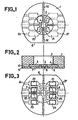
- Contact regions 20-25 are provided to allow access to the electrical terminals of the micro-box.
- a central zone serves as a substrate contact for the semiconductor circuit not shown in the drawing.
- This circuit is of substantially parallelepipedal form. Conductive wires are welded to the circuit to connect it electrically on one side or the other of the conductive pads 20-25, electrical access terminals of the microbatter.
- the electrical wires connecting in FIG. 2 for example the zone 5 to the semiconductor circuit arranged in the zone 4 are welded on the upper part of the support.
- the micro-housing includes an annular part 1 disposed above the support 11.
- this annular part is made of a plastic material which can be welded hot on the support 11.
- the annular case 1 produces a capsule which in particular makes it possible to trap part of the connections formed by conductive pads such as pads 22-25. A first effect of this box is therefore to improve the mechanical strength of these metal conductive pads produced on metal strips of very small thickness.
- the annular housing 1 also includes a central bore 2 through which the semiconductor circuit is deposited on the central zone 4. At the end of the process for manufacturing a micromodule, the inside of the hole 2 is loaded with a thermosetting resin . Another effect of the invention is thus to allow the shape of the drop of resin that the prior art learns to deposit on a semiconductor deposited on a conductive pad like track 4 to be precisely calibrated.
- the metal parts are entirely included inside the support and the housing 1. Only, bores such as bores 20-24, allow electrical access once the micromodule has been manufactured. In an alternative embodiment, a metallization of these holes is also carried out in order to allow better reading. This arrangement is favorable for avoiding the problems of detachment of the conductive pads upon reading.
- the conductive parts are produced by cuts or photoengravings in a metal strip.
- the cutouts are such that a particular connection drawing corresponding to the total desired circuit is drawn in addition to the additional lugs such as the lugs 26 and 27 on the conductive pads 20 and 21 of FIG. 1 are provided so as to reinforce the anchoring of each conductive tab in the micromodule.
- the central area is extended by legs 30-31.
Description
- La présente invention concerne un procédé de fabrication d'un microboitier. L'invention concerne aussi un microboitier à contacts effleurants. Elle concerne enfin une application d'un -tel microboitier à une carte contenant des composants de type CCC.
- Des microboitiers sont décrits dans les documents US-A 4 276 558 et GB-A 2 149 209.
- Une carte de type CCC, utilisée par exemple en paiement électronique comporte un support au format carte de crédit et implanté à la surface du support, un microboitier appelé aussi micromodule qui comporte à la fois la connectique, l'encapsulation et le circuit électronique de la carte.
- D'après l'art antérieur, on sait fabriquer des micromodules comportant sur un support des parties conductrices et un circuit semiconducteur par exemple sur substrat silicium. A la fin de l'opération de fabrication on dépose une goutte de résine thermodurcissable par dessus le circuit pour le protéger avec ses connexions et améliorer la rigidité mécanique du micromodule.
- Mais la viscosité des résines rend difficile la garantie de précisions suffisantes des dimensions de la goutte déposée. Or, le montage du micromodule dans la carte CCC, opération dite d'encartage, demande que certaines dimensions extérieures du micromodule soient respectées. Il faut en effet que le micromodule soit bien placé en profondeur dans la carte pour éviter de dépasser ou de former un creux. Dans la première situation, le micromodule peut être arraché à l'introduction de la carte dans le lecteur de cartes CCC. Dans la seconde situation, le creux est susceptible de créer une zone de colmatage pour les salissures qui peuvent alors masquer les contacts. Il faut aussi que le micromodule soit convenablement disposé dans le plan de la carte. En effet, les contacts du micromodule apparaissent à la surface de la carte et sont disposés pour être lus par des contacts d'un lecteur. On conçoit que la forme et les dimensions de la goutte de résine soient déterminantes pour la bonne qualité de la carte. Or, dans les procédé anciens, il faut rectifier la goutte par meulage et sa forme n'est pas réellement optimisée.
- Pour remédier à ces inconvénients, l'invention propose un procédé de fabrication d'un microboitier. Selon ce procédé on constitue sur un support isolant une succession de plages conductrices munies de zones de contact accessible de l'extérieur du microboitier. L'une de ces plages conductrices reçoit un circuit semiconducteur relié électriquement par des fils aux autres plages conductrices. Puis on dépose sur la face du support portant le circuit semiconducteur un boitier creux. Enfin on remplit le boitier creux d'une résine destinée à protéger le circuit semiconducteur et ces connexions.
- L'invention concerne aussi une nouvelle structure qui concerne un microboitier disposé sur un support et muni de contacts électriques reliés à un circuit semiconducteur porté par le support. Le microboitier selon l'invention comporte une capsule destinée à enrober une goutte de résine déposée par dessus le circuit de manière à en garantir la forme et les dimensions.
- D'autres avantages et caractéristiques de la présente invention seront mieux compris à l'aide de la description et des dessins qui sont :
- - la figure 1 : une vue de dessous d'un microboitier selon l'invention,
- - la figure 2 : la vue de face correspondante, en coupe,
- - la figure 3 : la vue de dessous correspondante. Sur les dessins, le microboitier a été figuré sans que le circuit et ses fils de liaison soient installés. Dans le procédé selon l'invention, on commence par fabriquer un module constitué d'un support et de contacts.
- Dans un mode de réalisation préféré, le module est réalisé à partir d'un film plastique métallisé. Par un procédé de gravure comme un procédé photochimique on dessine sur le film des zones de contacts en enlevant le métal largement entre ces zones. Des régions de contacts 20-25 sont ménagées pour permettre d'accéder aux bornes électriques du microboitier. Une zone centrale sert de contact de substrat au circuit semi-conducteur non représenté au dessin. Ce circuit est de forme sensiblement pa- rallèlépipédique. Des fils conducteurs sont soudés sur le circuit pour le relier électriquement sur une face ou l'autre des plages conductrices 20-25, bornes d'accès électrique du microboitier.
- Dans un exemple de réalisation les fils électriques reliant sur la figure 2 par exemple la zone 5 au circuit semiconducteur disposé sur la zone 4 sont soudés sur la partie supérieure du support. A la figure 2 on remarque que le microboitier comporte une partie annulaire 1 disposée au-dessus du support 11. Dans le procédé selon l'invention cette partie annulaire est réalisée en un matériau plastique qui peut se souder à chaud sur le support 11. Le boitier annulaire 1 réalise une capsule qui permet en particulier d'emprisonner une partie des connexions constituées par les plages conductrices comme les plages 22-25. Un premier effet de ce boitier est donc d'améliorer la tenue mécanique de ces plages conductrices métalliques réalisées sur des bandes métalliques de très faible épaisseur.
- Le boitier annulaire 1 comporte aussi un perçage 2 central à travers lequel le circuit semi-conducteur est déposé sur la zone centrale 4. A la fin du procédé de fabrication d'un micromodule, on charge l'intérieur du trou 2 avec une résine thermodurcissable. Un autre effet de l'invention est de permettre ainsi de calibrer exactement la forme de la goutte de résine que l'art antérieur apprend à déposer sur un semiconducteur déposé sur une plage conductrice comme la plage 4.
- On remarquera que, dans l'exemple de réalisation décrit, les parties métalliques sont entièrement incluses à l'intérieur du support et du boitier 1. Seuls, des perçages comme les perçages 20-24, permettent un accès électrique une fois le micromodule fabriqué. Dans une variante d'exécution une métallisation de ces perçages est réalisée en plus afin de permettre une meilleure lecture. Cette disposition est favorable pour éviter les problèmes de décollement des plages conductrices à la lecture.
- Selon une autre caractéristique de l'invention, les parties conductrices sont réalisées par des coupes ou photogravures dans une bande métallique. Les découpes sont telles que un dessin particulier de connexion correspondant au circuit total désiré est dessiné en plus des pattes supplémentaires comme les pattes 26 et 27 sur les plages conductrices 20 et 21 de la figure 1 sont prévues de manière à renforcer l'ancrage de chaque patte conductrice dans le micromodule. De même la zone centrale est prolongée par des pattes 30-31.
Claims (5)
Applications Claiming Priority (2)
| Application Number | Priority Date | Filing Date | Title |
|---|---|---|---|
| FR8515114A FR2588695B1 (fr) | 1985-10-11 | 1985-10-11 | Procede de fabrication d'un microboitier, microboitier a contacts effleurants et application aux cartes contenant des composants |
| FR8515114 | 1985-10-11 |
Publications (2)
| Publication Number | Publication Date |
|---|---|
| EP0226480A1 EP0226480A1 (fr) | 1987-06-24 |
| EP0226480B1 true EP0226480B1 (fr) | 1990-08-01 |
Family
ID=9323757
Family Applications (1)
| Application Number | Title | Priority Date | Filing Date |
|---|---|---|---|
| EP86402241A Expired - Lifetime EP0226480B1 (fr) | 1985-10-11 | 1986-10-09 | Procédé de fabrication d'un microboîtier, microboîtier à contacts effleurants, et application aux cartes contenant des composants |
Country Status (5)
| Country | Link |
|---|---|
| US (1) | US4864383A (fr) |
| EP (1) | EP0226480B1 (fr) |
| JP (1) | JPS62259461A (fr) |
| DE (1) | DE3673141D1 (fr) |
| FR (1) | FR2588695B1 (fr) |
Families Citing this family (19)
| Publication number | Priority date | Publication date | Assignee | Title |
|---|---|---|---|---|
| WO1990000813A1 (fr) * | 1988-07-08 | 1990-01-25 | Oki Electric Industry Co., Ltd. | Dispositif semi-conducteur |
| DE3924439A1 (de) * | 1989-07-24 | 1991-04-18 | Edgar Schneider | Traegerelement mit wenigstens einem integrierten schaltkreis, insbesondere zum einbau in chip-karten, sowie verfahren zur herstellung dieser traegerelemente |
| FR2671416B1 (fr) * | 1991-01-04 | 1993-04-23 | Solaic Sa | Procede pour la fabrication d'une carte a memoire et carte a memoire ainsi obtenue. |
| FR2673039A1 (fr) * | 1991-02-18 | 1992-08-21 | Em Microelectronic Marin Sa | Module protege pour carte a microcircuits. |
| FR2684236B1 (fr) * | 1991-11-27 | 1998-08-21 | Gemplus Card Int | Dispositif de connexion de circuit integre. |
| DE4224103A1 (de) * | 1992-07-22 | 1994-01-27 | Manfred Dr Ing Michalk | Miniaturgehäuse mit elektronischen Bauelementen |
| US6686226B1 (en) * | 1994-02-10 | 2004-02-03 | Hitachi, Ltd. | Method of manufacturing a semiconductor device a ball grid array package structure using a supporting frame |
| US5508231A (en) * | 1994-03-07 | 1996-04-16 | National Semiconductor Corporation | Apparatus and method for achieving mechanical and thermal isolation of portions of integrated monolithic circuits |
| EP0688051B1 (fr) * | 1994-06-15 | 1999-09-15 | De La Rue Cartes Et Systemes | Procédé de fabrication et d'assemblage de carte à circuit intégré. |
| FR2724477B1 (fr) * | 1994-09-13 | 1997-01-10 | Gemplus Card Int | Procede de fabrication de cartes sans contact |
| FR2748336A1 (fr) * | 1996-05-06 | 1997-11-07 | Solaic Sa | Carte a memoire a circuit integre enchasse dans le corps de carte |
| CN1134064C (zh) * | 1996-05-17 | 2004-01-07 | 西门子公司 | 半导体芯片用的载体元件 |
| FR2756648B1 (fr) * | 1996-11-29 | 1999-01-08 | Solaic Sa | Carte a memoire du type sans contact |
| US6109530A (en) * | 1998-07-08 | 2000-08-29 | Motorola, Inc. | Integrated circuit carrier package with battery coin cell |
| JP2003023134A (ja) * | 2001-07-09 | 2003-01-24 | Hitachi Ltd | 半導体装置およびその製造方法 |
| US8649820B2 (en) | 2011-11-07 | 2014-02-11 | Blackberry Limited | Universal integrated circuit card apparatus and related methods |
| USD703208S1 (en) | 2012-04-13 | 2014-04-22 | Blackberry Limited | UICC apparatus |
| US8936199B2 (en) | 2012-04-13 | 2015-01-20 | Blackberry Limited | UICC apparatus and related methods |
| USD701864S1 (en) * | 2012-04-23 | 2014-04-01 | Blackberry Limited | UICC apparatus |
Family Cites Families (10)
| Publication number | Priority date | Publication date | Assignee | Title |
|---|---|---|---|---|
| US4056681A (en) * | 1975-08-04 | 1977-11-01 | International Telephone And Telegraph Corporation | Self-aligning package for integrated circuits |
| US4138691A (en) * | 1977-06-07 | 1979-02-06 | Nippon Electric Co., Ltd. | Framed lead assembly for a semiconductor device comprising insulator reinforcing strips supported by a frame and made integral with lead strips |
| US4323914A (en) * | 1979-02-01 | 1982-04-06 | International Business Machines Corporation | Heat transfer structure for integrated circuit package |
| US4276558A (en) * | 1979-06-15 | 1981-06-30 | Ford Aerospace & Communications Corp. | Hermetically sealed active microwave integrated circuit |
| DE3019207A1 (de) * | 1980-05-20 | 1981-11-26 | GAO Gesellschaft für Automation und Organisation mbH, 8000 München | Traegerelement fuer einen ic-chip |
| DE3029667A1 (de) * | 1980-08-05 | 1982-03-11 | GAO Gesellschaft für Automation und Organisation mbH, 8000 München | Traegerelement fuer einen ic-baustein |
| FR2488732A1 (fr) * | 1980-08-18 | 1982-02-19 | Ebauchesfabrik Eta Ag | Procede de realisation de boitier pour composant electronique |
| DE3153768C2 (de) * | 1981-04-14 | 1995-11-09 | Gao Ges Automation Org | Ausweiskarte |
| DE3130213A1 (de) * | 1981-07-30 | 1983-02-17 | Siemens AG, 1000 Berlin und 8000 München | Verfahren zur herstellung einer tragbaren karte zur informationsverarbeitung |
| CA1204213A (fr) * | 1982-09-09 | 1986-05-06 | Masahiro Takeda | Carte a memoire protegee contre l'electricite statique |
-
1985
- 1985-10-11 FR FR8515114A patent/FR2588695B1/fr not_active Expired
-
1986
- 1986-10-02 US US06/914,418 patent/US4864383A/en not_active Expired - Lifetime
- 1986-10-09 EP EP86402241A patent/EP0226480B1/fr not_active Expired - Lifetime
- 1986-10-09 JP JP61239383A patent/JPS62259461A/ja active Pending
- 1986-10-09 DE DE8686402241T patent/DE3673141D1/de not_active Expired - Fee Related
Also Published As
| Publication number | Publication date |
|---|---|
| EP0226480A1 (fr) | 1987-06-24 |
| JPS62259461A (ja) | 1987-11-11 |
| US4864383A (en) | 1989-09-05 |
| FR2588695A1 (fr) | 1987-04-17 |
| FR2588695B1 (fr) | 1988-07-29 |
| DE3673141D1 (de) | 1990-09-06 |
Similar Documents
| Publication | Publication Date | Title |
|---|---|---|
| EP0226480B1 (fr) | Procédé de fabrication d'un microboîtier, microboîtier à contacts effleurants, et application aux cartes contenant des composants | |
| EP0391790B1 (fr) | Procédé de fabrication d'un module électronique | |
| EP0344058B2 (fr) | Procédé de réalisation d'une carte à mémoire électronique et carte à mémoire électronique obtenue par la mise en oeuvre dudit procédé | |
| US4774633A (en) | Method for assembling an integrated circuit with raised contacts on a substrate, device thereby produced and an electronic microcircuit card incorporating said device | |
| EP0254640B1 (fr) | Procédé de réalisation d'une carte à mémoire électronique et carte telle qu'obtenue par ce procédé | |
| EP0321340B1 (fr) | Support de composant électronique, notamment pour carte mémoire, et produit ainsi obtenu | |
| EP1012785B1 (fr) | Procede de fabrication de carte a antenne bobinee | |
| EP0593330A1 (fr) | Procédé d'interconnexion 3D de boîtiers de composants électroniques, et composant 3D en résultant | |
| EP0321326B1 (fr) | Procédé de mise en place sur un support, d'un composant électronique, muni de ses contacts | |
| EP0321327B1 (fr) | Procédé de mise en place d'un composant électronique et de ses connexions électriques sur un support | |
| EP0213974A1 (fr) | Micromodule à contacts enterrés et carte contenant des circuits comportant un tel micromodule | |
| EP0079265B1 (fr) | Procédé de réalisation d'un socle pour le montage d'une pastille semiconductrice sur l'embase d'un boîtier d'encapsulation | |
| EP1724712A1 (fr) | Micromodule, notamment pour carte à puce | |
| WO2000025265A1 (fr) | Procede de fabrication d'une carte a puce et d'un module electronique destine a etre insere dans une telle carte | |
| CA2293460A1 (fr) | Procede de fabrication de carte a puce sans contact | |
| FR2810768A1 (fr) | Procede de fabrication de cartes a puce hybrides et cartes a puce obtenues par ledit procede | |
| FR2601477A1 (fr) | Procede de montage d'un circuit integre dans une carte a microcircuits electroniques, et carte en resultant | |
| FR2795202A1 (fr) | Carte et procede de fabrication de cartes ayant une interface de communication a contact et sans contact | |
| FR3083892A1 (fr) | Carte a puce a double interface de communication et son procede de fabrication | |
| FR2817656A1 (fr) | Isolation electrique de microcircuits regroupes avant collage unitaire | |
| EP1210690B1 (fr) | Dispositif electronique comportant au moins une puce fixee sur un support et procede de fabrication d'un tel dispositif | |
| FR2796203A1 (fr) | Module electronique sans contact et procede pour son obtention | |
| WO2003038746A1 (fr) | Languette deformable integree a un module pour raccordement electrique a coeur | |
| FR2797976A1 (fr) | Procede de fabrication de cartes a puce hybrides et cartes a puce obtenues par ledit procede | |
| JPH09240176A (ja) | Icカード及びその製造方法 |
Legal Events
| Date | Code | Title | Description |
|---|---|---|---|
| PUAI | Public reference made under article 153(3) epc to a published international application that has entered the european phase |
Free format text: ORIGINAL CODE: 0009012 |
|
| AK | Designated contracting states |
Kind code of ref document: A1 Designated state(s): CH DE FR GB LI NL |
|
| 17P | Request for examination filed |
Effective date: 19871026 |
|
| 17Q | First examination report despatched |
Effective date: 19891123 |
|
| RAP1 | Party data changed (applicant data changed or rights of an application transferred) |
Owner name: THOMSON COMPOSANTS MILITAIRES ET SPATIAUX |
|
| GRAA | (expected) grant |
Free format text: ORIGINAL CODE: 0009210 |
|
| STAA | Information on the status of an ep patent application or granted ep patent |
Free format text: STATUS: THE PATENT HAS BEEN GRANTED |
|
| AK | Designated contracting states |
Kind code of ref document: B1 Designated state(s): CH DE FR GB LI NL |
|
| REF | Corresponds to: |
Ref document number: 3673141 Country of ref document: DE Date of ref document: 19900906 |
|
| GBT | Gb: translation of ep patent filed (gb section 77(6)(a)/1977) | ||
| PLBE | No opposition filed within time limit |
Free format text: ORIGINAL CODE: 0009261 |
|
| PLBI | Opposition filed |
Free format text: ORIGINAL CODE: 0009260 |
|
| 26N | No opposition filed | ||
| 26 | Opposition filed |
Opponent name: GAO GESELLSCHAFT FUER AUTOMATION UND ORGANISATION Effective date: 19910528 |
|
| NLR1 | Nl: opposition has been filed with the epo |
Opponent name: GAO GESELLSCHAFT FUER AUTOMATION AND ORGANISATION |
|
| PLBG | Opposition deemed not to have been filed |
Free format text: ORIGINAL CODE: 0009274 |
|
| 26D | Opposition deemed not to have been filed | ||
| NLXE | Nl: other communications concerning ep-patents (part 3 heading xe) |
Free format text: IN PAT.BUL.18/91:THE OPPOSITION SHOULD BE DEEMED NOT TO HAVE BEEN FILED |
|
| PLAA | Information modified related to event that no opposition was filed |
Free format text: ORIGINAL CODE: 0009299DELT |
|
| REG | Reference to a national code |
Ref country code: FR Ref legal event code: D6 |
|
| PGFP | Annual fee paid to national office [announced via postgrant information from national office to epo] |
Ref country code: DE Payment date: 20001002 Year of fee payment: 15 |
|
| PGFP | Annual fee paid to national office [announced via postgrant information from national office to epo] |
Ref country code: GB Payment date: 20001004 Year of fee payment: 15 |
|
| PGFP | Annual fee paid to national office [announced via postgrant information from national office to epo] |
Ref country code: CH Payment date: 20001011 Year of fee payment: 15 |
|
| PGFP | Annual fee paid to national office [announced via postgrant information from national office to epo] |
Ref country code: NL Payment date: 20001026 Year of fee payment: 15 |
|
| PG25 | Lapsed in a contracting state [announced via postgrant information from national office to epo] |
Ref country code: GB Free format text: LAPSE BECAUSE OF NON-PAYMENT OF DUE FEES Effective date: 20011009 |
|
| PG25 | Lapsed in a contracting state [announced via postgrant information from national office to epo] |
Ref country code: LI Free format text: LAPSE BECAUSE OF NON-PAYMENT OF DUE FEES Effective date: 20011031 Ref country code: CH Free format text: LAPSE BECAUSE OF NON-PAYMENT OF DUE FEES Effective date: 20011031 |
|
| REG | Reference to a national code |
Ref country code: GB Ref legal event code: IF02 |
|
| PG25 | Lapsed in a contracting state [announced via postgrant information from national office to epo] |
Ref country code: NL Free format text: LAPSE BECAUSE OF NON-PAYMENT OF DUE FEES Effective date: 20020501 |
|
| GBPC | Gb: european patent ceased through non-payment of renewal fee |
Effective date: 20011009 |
|
| REG | Reference to a national code |
Ref country code: CH Ref legal event code: PL |
|
| NLV4 | Nl: lapsed or anulled due to non-payment of the annual fee |
Effective date: 20020501 |
|
| PG25 | Lapsed in a contracting state [announced via postgrant information from national office to epo] |
Ref country code: DE Free format text: LAPSE BECAUSE OF NON-PAYMENT OF DUE FEES Effective date: 20020702 |
|
| PGFP | Annual fee paid to national office [announced via postgrant information from national office to epo] |
Ref country code: FR Payment date: 20021008 Year of fee payment: 17 |
|
| PG25 | Lapsed in a contracting state [announced via postgrant information from national office to epo] |
Ref country code: FR Free format text: LAPSE BECAUSE OF NON-PAYMENT OF DUE FEES Effective date: 20040630 |
|
| REG | Reference to a national code |
Ref country code: FR Ref legal event code: ST |
|
| RIN2 | Information on inventor provided after grant (corrected) |
Inventor name: PERES, PHILIPPE Inventor name: GLOTON, JEAN-PIERRE |