EP0225644A2 - Leistungsversorgungsschalterschaltung zum Gebrauch in einem Sender-Empfänger oder dergleichen - Google Patents
Leistungsversorgungsschalterschaltung zum Gebrauch in einem Sender-Empfänger oder dergleichen Download PDFInfo
- Publication number
- EP0225644A2 EP0225644A2 EP86117214A EP86117214A EP0225644A2 EP 0225644 A2 EP0225644 A2 EP 0225644A2 EP 86117214 A EP86117214 A EP 86117214A EP 86117214 A EP86117214 A EP 86117214A EP 0225644 A2 EP0225644 A2 EP 0225644A2
- Authority
- EP
- European Patent Office
- Prior art keywords
- voltage
- source
- enhancement mode
- mode mos
- mos fet
- Prior art date
- Legal status (The legal status is an assumption and is not a legal conclusion. Google has not performed a legal analysis and makes no representation as to the accuracy of the status listed.)
- Granted
Links
Images

Classifications
-
- H—ELECTRICITY
- H02—GENERATION; CONVERSION OR DISTRIBUTION OF ELECTRIC POWER
- H02M—APPARATUS FOR CONVERSION BETWEEN AC AND AC, BETWEEN AC AND DC, OR BETWEEN DC AND DC, AND FOR USE WITH MAINS OR SIMILAR POWER SUPPLY SYSTEMS; CONVERSION OF DC OR AC INPUT POWER INTO SURGE OUTPUT POWER; CONTROL OR REGULATION THEREOF
- H02M3/00—Conversion of DC power input into DC power output
- H02M3/02—Conversion of DC power input into DC power output without intermediate conversion into AC
- H02M3/04—Conversion of DC power input into DC power output without intermediate conversion into AC by static converters
- H02M3/06—Conversion of DC power input into DC power output without intermediate conversion into AC by static converters using resistors or capacitors, e.g. potential divider
- H02M3/07—Conversion of DC power input into DC power output without intermediate conversion into AC by static converters using resistors or capacitors, e.g. potential divider using capacitors charged and discharged alternately by semiconductor devices with control electrode, e.g. charge pumps
Definitions
- the present invention relates to a power switch circuit and, more particularly, to a switch circuit for on-off controlling a power supply to a load, such as a transmitting/receiving portion of a radio transmitter/ receiver to be referred to as a transceiver hereinafter.
- a typical example of a conventional power switch circuit of this type is disclosed in U. S. Patent No. 4,420,700 issued to Fay et al on December 13, 1983.
- the switch circuit disclosed in this patent includes an N channel enhancement metal-oxide semiconductor field effect transistor (MOS FET) arranged between a power supply and a load, such as a transmitting/receiving portion etc. of a transceiver. Since a gate drive current of a MOS FET is as small as 1 microampere or less and a tolerable current therethrough can be made relatively large without increasing a size thereof, in general, the disclosed switch circuit is compact and a current consumption thereof is small enough.
- MOS FET N channel enhancement metal-oxide semiconductor field effect transistor
- the power source becomes always connected to the load such as the transmitting/receiving portion, causing the load to be broken down or a performance thereof to be degraded.
- an object of the present invention is to provide a power switch circuit which is compact in size and has a minimized current consumption and which the breakdown of a load and/or degradation of performance thereof is prevented from occurring even when the power source is connected to the transceiver with terminals being reversed.
- a power switch circuit comprising: a power source for providing a direct current (DC) voltage; a voltage booster circuit for boosting the DC voltage; a switch connected between the power source and the voltage booster circuit for on-off controlling the latter; a first enhancement mode MOS FET having the drain or source connected to the power source and the gate connected to the output of the voltage booster circuit; a second enhancement mode MOS FET having the source or drain connected to the source or drain of the first enhancement MOS FET and the gate connected to the output of the voltage booster circuit; and means for connecting the source or drain of the second enhancement mode MOS FET to a load.
- DC direct current
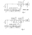
- a conventional power switch circuit will be described firstly with reference to Fig. 1.
- the power switch circuit shown in Fig. 1 is substantially the same as that disclosed in the aforementioned U. S. Patent to Fay et al.
- a power source or battery 1 connected through a switch composed of an N channel enhancement mode MOS FET 3 to a transmitting/receiving portion 2 acting as a load.
- the power source 1 is intended to supply a direct current (DC) to the load 2.
- the drain D, the source S and the gate G of the MOS FET 3 are connected to the positive terminal of the power source 1, the transmitting/ receiving portion 2 and a booster circuit 8, respectively.
- the booster circuit 8 is composed of an oscillator 6 and a multistage voltage doubling and rectifying circuit 7 and adapted to boost a source voltage supplied through a power switch 5 from the power source 1 and to supply a resulting high voltage to the gate G of the MOS FET 3.
- the source voltage of the power source 1 is boosted by the booster circuit 8 and applied to the.gate G of the MOS FET 3 to turn the latter on.
- the voltage of power source 1 is applied to the transmitting/ receiving portion 2.
- the transmitting/receiving portion 2 requires a current of 2 to 3 amperes for an output power of 5 watts when applied to a mobile station of a mobile telecommunication system having a frequency band of 800 MHz, for example.
- a tolerable current of the MOS FET covers this current value sufficiently.
- parasitic diode 31 formed between the drain D and the source S of the MOS FET 3, through which a current tends to flow from the source side to the drain side regardless of the on-off operation of the power switch 5 when the connections of the positive and negative terminals of the power source 1 to the FET are reversed erroneously, as mentioned previously. Such current flow in the reverse direction may damage the transmitting/ receiving portion 2 or degrade the performance thereof.
- a MOS FET 4 is added in series with the MOS FE T 3, which is of the same type as that of the MOS FET 3 and connected between the latter and the transmitting/receiving portion 2 with a source S and a drain D being reversed with respect to those.of the MOS FET 3. That is, the source S and the drain D of the MOS FET 4'are.connected to the source S of the MOS FET 3 and the transmitting/ receiving portion 2, respectively.
- a gate G of the MOS FET 4 is connected to the gate of the MOS FET 3 and supplied with the same output voltage of a booster circuit 18.
- a MOS FET having the source S and the drain D connected so as to allow a.current to flow from the source S to the drain D can be on-off controlled according to a gate voltage.thereof. Therefore, even with the MOS FETs 3 and 4 connected as shown, a power can be supplied from the power source 1 to the transmitting/ receiving portion 2 when the switch 5 is turned on.
- a gate voltage required to turn-on the MOS FET is about 30 volts when the power source voltage is 13.8 volts.
- the MOS FET.4 has a parasitic diode 41 formed between the source S and the drain D thereot.
- the parasitic diodes 31 and 41 are connected in opposite polarity. Therefore, there is no current allowed to flow between the power source 1 and the transmitting/receiving portion 2 when the positive and negative terminals of the power source 1 are connected to the circuit erroneously in polarity. Consequently, it is possible to prevent the damage or degradation of performance of the transmitting/ receiving portion 2 due to the reversed connection of the power source thereto.
- Fig. 3 shows the booster circuit 18 of the embodiment shown in Fig. 2, in detail.
- the booster circuit 18 comprises an oscillator 16 and a voltage up-converter 17.
- the oscillator 16 comprises an astable multivibrator composed of a pair of transistors Trl and Tr2.
- Trl or Tr2 When the switch 5 is turned on, either the transistor Trl or Tr2 is turned on in an initial stage since the oscillator 16 is astable. Assuming that the transistor Tr2 is turned on. The emitter and collector voltages of transistor Tr2 and the emitter and base voltages of transistor Trl have the same voltage and thus the transistor Trl is in the off state. As long as the on-state of transistor Tr2 continues, a capacitor C2 is charged gradually in the positive direction through a resistor R3.
- the transistor Trl When the terminal voltage of capacitor C2 reaches 0.7 volts, the transistor Trl is turned on and the transistor Tr2 is turned off in the same way as the transistor Trl. With the repetition of this operation, the collector voltage of transistor Tr2, i.e., the output of oscillator 16 becomes a rectangular signal having peak values zero and V volts, where V is the voltage of power source 1.
- a voltage up-converter 17 comprises a multistage voltage doubling and smoothing circuit in the form of the so-called Cockcroft-Walton circuit.
- a current flows through a diode Xl and a capacitor C3 and charges the latter with the peak voltage V volts of the oscillation voltage.
- a current flows through the capacitor C3, a diode X2 and a capacitor C4. Therefore, the latter capacitor is charged with a voltage which is a charge voltage, V volts, of the capacitor C3 added by the oscillation voltage, zero volt, providing a terminal voltage of V volts.
- a current flows through a capacitor C4, a diode X3, a capacitor C5 and the capacitor C3 to charge the capacitor C5 with a voltage which is the charge voltage, V volts, of the capacitor C 4 added by the oscillation voltage, V volts, resulting in a terminal voltage of 2V volts.
- a terminal voltage of a capacitor C8 in the last stage becomes 3V volts.
- Fig. 4 shows another embodiment of the present invention.
- the composition of Fig. 4 differs from that of Fig. 2 in that the connection of the MOS FETs 3 and 4 is reversed. That is, the drains of the MOS FETs 3 and 4 are connected together. Also in this case, there is no current to flow between the power source 1 and the transmitting/receiving portion 2 through the parasitic diodes when the power.source is connected with polarity being reversed erroneously.
- the power switch circuit according to the present invention includes a pair of enhancement mode MOS FETs arranged between the power source and the load with the sources or the drains thereof being connected together. Due to the employment of the enhancement mode MOS FETs, the power switch circuit can be compact in size and the power consumption thereof is minimized. Further, even if the power source is connected erroneously to the load with reversed polarity, there is no damage of the load or no degradation of performance thereof.
Landscapes
- Engineering & Computer Science (AREA)
- Power Engineering (AREA)
- Electronic Switches (AREA)
- Transceivers (AREA)
- Dc-Dc Converters (AREA)
- Direct Current Feeding And Distribution (AREA)
Applications Claiming Priority (2)
| Application Number | Priority Date | Filing Date | Title |
|---|---|---|---|
| JP60278546A JPS62137925A (ja) | 1985-12-11 | 1985-12-11 | 無線送受信機 |
| JP278546/85 | 1985-12-11 |
Publications (3)
| Publication Number | Publication Date |
|---|---|
| EP0225644A2 true EP0225644A2 (de) | 1987-06-16 |
| EP0225644A3 EP0225644A3 (en) | 1988-09-07 |
| EP0225644B1 EP0225644B1 (de) | 1992-03-18 |
Family
ID=17598762
Family Applications (1)
| Application Number | Title | Priority Date | Filing Date |
|---|---|---|---|
| EP86117214A Expired - Lifetime EP0225644B1 (de) | 1985-12-11 | 1986-12-10 | Leistungsversorgungsschalterschaltung zum Gebrauch in einem Sender-Empfänger oder dergleichen |
Country Status (5)
| Country | Link |
|---|---|
| EP (1) | EP0225644B1 (de) |
| JP (1) | JPS62137925A (de) |
| AU (1) | AU596135B2 (de) |
| CA (1) | CA1260543A (de) |
| DE (1) | DE3684419D1 (de) |
Cited By (3)
| Publication number | Priority date | Publication date | Assignee | Title |
|---|---|---|---|---|
| EP0645751A1 (de) * | 1993-08-31 | 1995-03-29 | Sharp Kabushiki Kaisha | Einrichtung zur Steuerspannungserzeugung für eine Flüssigkristallanzeigeeinrichtung |
| EP1458112A4 (de) * | 2002-05-31 | 2004-11-24 | Matsushita Electric Industrial Co Ltd | Hochfrequenz-schaltnetzwerk und mobilkommunikationsendgerät damit |
| EP2881831A1 (de) * | 2013-12-06 | 2015-06-10 | Conti Temic microelectronic GmbH | Gleichspannungswandler und dessen Verwendung |
Family Cites Families (5)
| Publication number | Priority date | Publication date | Assignee | Title |
|---|---|---|---|---|
| US3820004A (en) * | 1972-02-02 | 1974-06-25 | Nippon Denso Co | Direct current voltage supply apparatus |
| US4420700A (en) * | 1981-05-26 | 1983-12-13 | Motorola Inc. | Semiconductor current regulator and switch |
| US4438356A (en) * | 1982-03-24 | 1984-03-20 | International Rectifier Corporation | Solid state relay circuit employing MOSFET power switching devices |
| GB2132447B (en) * | 1982-12-04 | 1986-07-30 | Standard Telephones Cables Ltd | Switch device |
| JPS60235531A (ja) * | 1984-05-08 | 1985-11-22 | Nec Corp | 無線送受信機 |
-
1985
- 1985-12-11 JP JP60278546A patent/JPS62137925A/ja active Granted
-
1986
- 1986-12-10 CA CA000524885A patent/CA1260543A/en not_active Expired
- 1986-12-10 EP EP86117214A patent/EP0225644B1/de not_active Expired - Lifetime
- 1986-12-10 DE DE8686117214T patent/DE3684419D1/de not_active Expired - Lifetime
- 1986-12-10 AU AU66376/86A patent/AU596135B2/en not_active Ceased
Cited By (6)
| Publication number | Priority date | Publication date | Assignee | Title |
|---|---|---|---|---|
| EP0645751A1 (de) * | 1993-08-31 | 1995-03-29 | Sharp Kabushiki Kaisha | Einrichtung zur Steuerspannungserzeugung für eine Flüssigkristallanzeigeeinrichtung |
| US5510814A (en) * | 1993-08-31 | 1996-04-23 | Sharp Kabushiki Kaisha | Drive voltage generating device for liquid crystal display device |
| EP1458112A4 (de) * | 2002-05-31 | 2004-11-24 | Matsushita Electric Industrial Co Ltd | Hochfrequenz-schaltnetzwerk und mobilkommunikationsendgerät damit |
| US7020453B2 (en) | 2002-05-31 | 2006-03-28 | Matsushita Electric Industrial Co., Ltd. | High-frequency switch circuit and mobile telecommunications terminal device using the same |
| EP1705805A3 (de) * | 2002-05-31 | 2006-12-20 | Matsushita Electric Industrial Co., Ltd. | Hochfrequenz-Schaltnetzwerk und Mobilkommunikationsendgerät damit |
| EP2881831A1 (de) * | 2013-12-06 | 2015-06-10 | Conti Temic microelectronic GmbH | Gleichspannungswandler und dessen Verwendung |
Also Published As
| Publication number | Publication date |
|---|---|
| AU596135B2 (en) | 1990-04-26 |
| JPH0466412B2 (de) | 1992-10-23 |
| CA1260543A (en) | 1989-09-26 |
| EP0225644A3 (en) | 1988-09-07 |
| EP0225644B1 (de) | 1992-03-18 |
| DE3684419D1 (de) | 1992-04-23 |
| AU6637686A (en) | 1987-06-18 |
| JPS62137925A (ja) | 1987-06-20 |
Similar Documents
| Publication | Publication Date | Title |
|---|---|---|
| JP2815838B2 (ja) | 高圧側スイッチに対する改善されたチャージポンプ回路 | |
| US4736121A (en) | Charge pump circuit for driving N-channel MOS transistors | |
| EP0079937B1 (de) | Halbleiterstromregulierung und schalter | |
| EP0112119B1 (de) | Gleichrichterbrückenschaltung | |
| US4553082A (en) | Transformerless drive circuit for field-effect transistors | |
| US12015349B2 (en) | Switching circuit, DC/DC converter, and control circuit thereof | |
| EP0717497A3 (de) | Zusammengesetzter Leistungs-MOSFET | |
| US4459539A (en) | Charge transfer constant volt-second regulator | |
| EP0559996B1 (de) | Treiber, insbesondere für Leistungs-MOS-Halbbrücken | |
| US4607210A (en) | Potential free actuation circuit for a pulse duration controlled electronic power switch | |
| EP0853365B1 (de) | Batterieladeeinheit | |
| GB2180422A (en) | Driving circuit for n-channel power mos transistors of push-pull stages | |
| EP0945986A3 (de) | Ladungspumpenschaltung für eine Phasenregelschleife | |
| EP0342581B1 (de) | Spannungspegelverwandlungsschaltung | |
| US5381044A (en) | Bootstrap circuit for driving a power MOS transistor | |
| US5914619A (en) | Trigger circuit for a power fet having a source-side load | |
| US6429635B2 (en) | Drive circuit for insulated gate type FETs | |
| EP0225644B1 (de) | Leistungsversorgungsschalterschaltung zum Gebrauch in einem Sender-Empfänger oder dergleichen | |
| US6169431B1 (en) | Drive circuit for a controllable semiconductor component | |
| US12003180B2 (en) | Power supply for driving synchronous rectification elements of SEPIC converter | |
| US6940732B2 (en) | Synchronous rectifier circuit | |
| EP0177148A2 (de) | Leistungsversorgung mit MOSFET-Elementen | |
| JP3003437B2 (ja) | 電圧変換装置 | |
| GB2339638A (en) | A high-side driver charge pump with a supply cutoff transistor | |
| KR20000016476A (ko) | 전압 극 전환 회로 |
Legal Events
| Date | Code | Title | Description |
|---|---|---|---|
| PUAI | Public reference made under article 153(3) epc to a published international application that has entered the european phase |
Free format text: ORIGINAL CODE: 0009012 |
|
| 17P | Request for examination filed |
Effective date: 19861210 |
|
| AK | Designated contracting states |
Kind code of ref document: A2 Designated state(s): DE FR GB NL SE |
|
| PUAL | Search report despatched |
Free format text: ORIGINAL CODE: 0009013 |
|
| AK | Designated contracting states |
Kind code of ref document: A3 Designated state(s): DE FR GB NL SE |
|
| 17Q | First examination report despatched |
Effective date: 19900823 |
|
| GRAA | (expected) grant |
Free format text: ORIGINAL CODE: 0009210 |
|
| AK | Designated contracting states |
Kind code of ref document: B1 Designated state(s): DE FR GB NL SE |
|
| REF | Corresponds to: |
Ref document number: 3684419 Country of ref document: DE Date of ref document: 19920423 |
|
| ET | Fr: translation filed | ||
| PLBI | Opposition filed |
Free format text: ORIGINAL CODE: 0009260 |
|
| PLAB | Opposition data, opponent's data or that of the opponent's representative modified |
Free format text: ORIGINAL CODE: 0009299OPPO |
|
| 26 | Opposition filed |
Opponent name: PHILIPS PATENTVERWALTUNG GMBH Effective date: 19921212 |
|
| R26 | Opposition filed (corrected) |
Opponent name: PHILIPS PATENTVERWALTUNG GMBH Effective date: 19921212 |
|
| NLR1 | Nl: opposition has been filed with the epo |
Opponent name: PHILIPS PATENTVERWALTUNG GMBH |
|
| PGFP | Annual fee paid to national office [announced via postgrant information from national office to epo] |
Ref country code: SE Payment date: 19931201 Year of fee payment: 8 |
|
| PGFP | Annual fee paid to national office [announced via postgrant information from national office to epo] |
Ref country code: GB Payment date: 19931208 Year of fee payment: 8 |
|
| PGFP | Annual fee paid to national office [announced via postgrant information from national office to epo] |
Ref country code: FR Payment date: 19931215 Year of fee payment: 8 |
|
| PGFP | Annual fee paid to national office [announced via postgrant information from national office to epo] |
Ref country code: NL Payment date: 19931231 Year of fee payment: 8 |
|
| PGFP | Annual fee paid to national office [announced via postgrant information from national office to epo] |
Ref country code: DE Payment date: 19940225 Year of fee payment: 8 |
|
| PG25 | Lapsed in a contracting state [announced via postgrant information from national office to epo] |
Ref country code: SE Effective date: 19941211 |
|
| EAL | Se: european patent in force in sweden |
Ref document number: 86117214.6 |
|
| RDAG | Patent revoked |
Free format text: ORIGINAL CODE: 0009271 |
|
| STAA | Information on the status of an ep patent application or granted ep patent |
Free format text: STATUS: PATENT REVOKED |
|
| 27W | Patent revoked |
Effective date: 19950225 |
|
| GBPR | Gb: patent revoked under art. 102 of the ep convention designating the uk as contracting state |
Free format text: 950225 |
|
| NLR2 | Nl: decision of opposition | ||
| EUG | Se: european patent has lapsed |
Ref document number: 86117214.6 |