EP0224946A2 - Method for identifying coins - Google Patents
Method for identifying coins Download PDFInfo
- Publication number
- EP0224946A2 EP0224946A2 EP19860201826 EP86201826A EP0224946A2 EP 0224946 A2 EP0224946 A2 EP 0224946A2 EP 19860201826 EP19860201826 EP 19860201826 EP 86201826 A EP86201826 A EP 86201826A EP 0224946 A2 EP0224946 A2 EP 0224946A2
- Authority
- EP
- European Patent Office
- Prior art keywords
- coin
- counter
- attenuation
- signal
- measurements
- Prior art date
- Legal status (The legal status is an assumption and is not a legal conclusion. Google has not performed a legal analysis and makes no representation as to the accuracy of the status listed.)
- Granted
Links
Images


Classifications
-
- G—PHYSICS
- G07—CHECKING-DEVICES
- G07D—HANDLING OF COINS OR VALUABLE PAPERS, e.g. TESTING, SORTING BY DENOMINATIONS, COUNTING, DISPENSING, CHANGING OR DEPOSITING
- G07D5/00—Testing specially adapted to determine the identity or genuineness of coins, e.g. for segregating coins which are unacceptable or alien to a currency
- G07D5/08—Testing the magnetic or electric properties
-
- G—PHYSICS
- G07—CHECKING-DEVICES
- G07D—HANDLING OF COINS OR VALUABLE PAPERS, e.g. TESTING, SORTING BY DENOMINATIONS, COUNTING, DISPENSING, CHANGING OR DEPOSITING
- G07D5/00—Testing specially adapted to determine the identity or genuineness of coins, e.g. for segregating coins which are unacceptable or alien to a currency
- G07D5/02—Testing the dimensions, e.g. thickness, diameter; Testing the deformation
Definitions
- the present invention relates to a method and apparatus for identifying coins including guidance of a coin through a passage in which certain properties of the coin are measured by an electromagnetic device, and where a number of measurements are taken at different positions of the coin within the passage.
- Coin filters are previously known from e.g. - UK Pat. No. 1.551.209 describes a device for checking metal pieces, particularly coins, by which electromagnetic response is measured at predetermined periods of time, related to the speed at which the coin passes the detector.
- - UK Pat. Appl. No. 2.107.104 describes a coin identification apparatus having an inductive coil wound on a ferrite core having two poles adapted in size and location to the coin types to be detected.
- a coin filter which is independent of the time it takes for a coin to pass a detector. It is simple in that it uses only one set of electromagnetic coils for taking a plurality of successive electromagnetic measurements of each coin. The coin positions at which the measurements are taken are determined by the coin itself.
- the coin interrupts a number of light channels 3, 4, 5 before passing the center of pair of coils 6.
- the reduction of the coupling between coils are measured a number of times with the coin in different positions controlled by the light channels.
- the coupling between the coils 6 will first be described.
- a sinusoidal signal E is emitted by one coil CE.
- CE coils
- the amplitude of the received signal R is determined by the coupling factor of the two coils.
- the received signal is attenuated.
- the difference in amplitude (attenuation Ai) on the received signal is the results (A1, A2, A3, ... An and Amax) which are measured for different positions of the coin.
- the light channels 3, 4, 5 are placed in different heights over the ramp 2 and in different distance from the coil center.
- the light channels should be placed so that no channels simultaneously hit the trailing edge of any passing coin.
- the "rate" of attenuation change will be measured in addition to the maximum attenuation. This gives an indication of the stamp of the coin.
- the largest and normally most valuable coins will break most of the light channels and thereby give relevant measurements.
- the first measurement should preferably show the smallest attenuation.
- the light channels should be arranged so that at least 1% (preferably between 1 - 20%) of the coin area is within the sensitive part of the coil when the first measurement is taken.
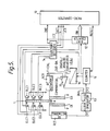
- the block diagram of a coin identifier circuit is given in fig. 5 (In the following description the number of light channels is set to three).
- the coin identifier includes a micro computer 10 having the following control lines: LC1, LC2 and LC3: Light channel selection RESET: Reset line for resetting an 8 bit counter 11 after completion of measurements.
- DATA BUS DB
- All measured results A1, A2, ...) are transmitted to the micro computer 10 via 8 output lines from an 8 bit port 12.
- INTERRUPT INT: This line signals (INT) to the micro-computer 10 that a result is present at the port 12.
- the counter 11 counts the number of pulses seen on a line CP2 from a clock pulse generator 13. This is a direct binary measure of attenuation Ai.
- Selection of light channels ELC1-3, RLC1-3 is made in a selector/decoder 14 by the micro computer 10 via the control lines LC1, LC2 and LC3, which are enabled when the counter 11 goes from its reset rest position.
- the receiver part of the selector/decoder 14 sends the signal INT to the micro computer 10 for each position of the coin where the results are to be read from the port 12.
- the signal INT is present the contents of the port 12 is latched.
- the clock pulse generator 13 supplies the transmitting or emitting coil CE with an alternating voltage CP1 which is made sinusoidal by an RC-network RCE.
- the generator also loads the counter 11 with clock pulses CP2 when not inhibited by a comparator 15.
- the generator 13 is provided with a pulse stretching arrangement for the inhibiting signal INH from the comparator 15.
- the contents of the counter 11 is transmitted to the micro-computer 10 via the port 12.
- the signal INT goes “low”
- the contents are latched.
- With a "high” on the INT line the counter contents is transmitted directly to the data bus DB.
- a digital/analog converter (D/A) 16 translates the binary contents of the counter 11 into an analog signal which is fed to the comparator 15.
- the level of the received signals OUT-COIL from the received coil CR is compared with the output OUT-DA from the D/A converter 16, confer Fig. 6.
- the comparator output INH becomes low. In rest position this will happen for every negative half wave of the OUT-COIL signal.
- the pulse stretcher in the clock pulse generator 13 covers the period between half waves, and as long pulses arrive with short intervals (see Figure 6), the clock pulse CP2 to the counter 11 is inhibited.
- the clock pulse signal CP2 is no longer inhibited and the counter 11 starts counting.
- the contents of this counter is now converted into an analog signal via the D/A converter 16. Since the binary input of the D/A converter 16 increases, its output signal OUT-DA will increase too.
- the signal OUT-DA will follow the attenuated amplitude of the received signal until the maximum attenuation is reached. Once this level has been reached by OUT-DA, the amplitude of the signal OUT-COIL starts increasing and the negative half wave of the signal will go below OUT-DA again. As a consequence the INH-line will start pulsing again, CP2 is inhibited and the counter stops in the position it reached and remains stable. The contents of the counter is a number indicating the maximum attenuation for the coin and OUT-DA remains stable at the maximum attenuation level. Also the information from the port 12 to the DB line remains stable at its highest value for the particular coin.
- the INT signal disappears so that the port 12 is opened for new data and ELC2 is on.
- the counter will continue to run as the coin passes the coil on its way to the maximum attenuation position.
- RLC2 receives light
- the contents of the port 12, which reads the accumulated number in the counter 11 will again be latched
- a new INT signal causes the micro computer 10 to read the port 12, store the result as "RESULT SECOND ATTENUATION" A2 and change the high level signal from LC2 to LC3.
- the high level signal on LC3 is removed, and the INT signal disappears so that the port 12 is again opened for new data.
- the micro computer 10 waits for the maximum attenuation level for the particular coin by checking the contents of the counter 11 via the port 12 every 8 msec. When two successive measurements show that the counter contents remain unchanged (different from zero), the port contents is stored as "RESULT MAX. ATTENUATION" (Amax). After that the counter 11 is reset and a high level signal is put onto LC1, waiting for the next coin. The emitter ELC1 is, however, not lit before a new coin starts attenuating the coil signals.
- Fig. 7 shows the attenuation as represented by the OUT-COIL signal occurring during the passage AM of the coin.
- the clock pulses CP2 to the counter 11 are also indicated as well as the positions on the OUT-COIL envelope curve where the attenuation measurements A1, A2, A3 and Amax are taken.
- the OUT-DA signal will go low as soon as the counter 11 is reset.
- the maximum attenuation (Result Amax) has a correlation to the other measured attenuations, (Result A1, A2 and A3) determined by the geometry and stamp of the coin,the difference between the adjoining results will be represented by a much narrower Gauss distribution curve for a random sample, than the maximum result Amax would give alone.
- the measured values may be combined in many ways. A high selectivity may be obtained by using two calculated values Amax-A3 and A3-A2 in addition to three of the initial measured results (A1, A2, and Amax).
- Setting of the limits can be done by inserting a random sample of a coin type in the coin identifier.
- the result of the different measurements for this sample can then be represented by Gauss distributions characterised by mean value ( ⁇ ) and standard deviation (d).
- the limits for the five results are then calculated (e.g. ⁇ 2d) and stored in an EPROM.
- a "flow chart" of the present invention can be listed as follows: - Counter is reset, - lights are off - Un-attenuated signal is received by receiver coil - Coin enters between coils - The signal starts getting attenuated - The counter starts counting, not time, but stepwise (incrementals) increases in attenuation - Light channel 1 is turned on - Coin blocks light - Coin opens for light - Counter status is registered (A1) - Light channel 1 is turned off - Light channel 2 is turned on - Coin opens for light - Counter status is registered (A2) - Light channel 2 is turned off - Counter contents are continuously cheched to find maximum attenuation - Max attenuation is found - Counter status is registered (Amax) - Counter is reset - Registered numbers (A1, A2 .... Amax) are evaluated individually and/or in combination. - Coin is accepted or rejected. - Ready for new coin Smaller coins do not block for light channel 1 (and 2). The results A1 (and A2) are registered immediately in the
Abstract
Description
- The present invention relates to a method and apparatus for identifying coins including guidance of a coin through a passage in which certain properties of the coin are measured by an electromagnetic device, and where a number of measurements are taken at different positions of the coin within the passage. Coin filters are previously known from e.g.
- UK Pat. No. 1.551.209 describes a device for checking metal pieces, particularly coins, by which electromagnetic response is measured at predetermined periods of time, related to the speed at which the coin passes the detector.
- UK Pat. Appl. No. 2.107.104 describes a coin identification apparatus having an inductive coil wound on a ferrite core having two poles adapted in size and location to the coin types to be detected. The coins's effect on the electromagnetic field is measured when the coin is between poles and when it is adjacent each pole face.
- UK Pat. Appl. No. 2.086.633 describes a coin sorting apparatus having a combination of electromagnetic and photoelectric sensors for judging between coins of different permeability.
- DE-OS No- 2.716.740 describes a device including a complicated system of capacitive, inductive and photoelectric sensors for identifying coins. - These known methods are considered to give rather unreliable results and the object of the present invention is to overcome the drawbacks of the known coin filters.
- The main features of the present invention are defined in the claims.
- With the present invention there is obtained a coin filter which is independent of the time it takes for a coin to pass a detector. It is simple in that it uses only one set of electromagnetic coils for taking a plurality of successive electromagnetic measurements of each coin. The coin positions at which the measurements are taken are determined by the coin itself.
- Above mentioned and other features and objects of the present invention will clearly appear from the following detailed description of embodiments of the invention taken in conjunction with the drawings, where
- - Fig. 1 illustrates the general principles of the coin edge detecting means related to a set of coupled coils
- - Figures 2 and 3 illustrate the coil input and output signals occuring in a rest mode and in an activated mode,
- - Fig. 4 illustrates the effect of placing a coin edge detector close to the top of the coin,
- - Fig. 5 shows a schematical block diagram of a coin identifying circuit
- Fig. 6 shows voltages of significant signals occuring in the circuit of Fig. 5, and
- - Fig. 7 illustrates the intermediate stored results of the coin identifier.
- The general principles are illustrated in Fig. 1. All introduced coins 1 are running down a ramp 2 and all measurements are performed dynamically within a short time and using a minimum of power.
- The coin interrupts a number of
light channels 3, 4, 5 before passing the center of pair of coils 6. - The reduction of the coupling between coils are measured a number of times with the coin in different positions controlled by the light channels.
- The principles of measurements are illustrated in Figures 2-4.
- The coupling between the coils 6 will first be described. A sinusoidal signal E is emitted by one coil CE. When no coin is in between the coils (CE, CR) the signal is received un-attenuated. The amplitude of the received signal R is determined by the coupling factor of the two coils. When a coin comes in between the two coils (CE, CR). the received signal is attenuated.
- The difference in amplitude (attenuation Ai) on the received signal is the results (A1, A2, A3, ... An and Amax) which are measured for different positions of the coin.
- The
light channels 3, 4, 5 are placed in different heights over the ramp 2 and in different distance from the coil center. The light channels should be placed so that no channels simultaneously hit the trailing edge of any passing coin. For each diameter of the different coins there should be a light channel positioned close to the top of the coin, say at a position higher than 80% of the coin diameter. By making a coupling measurement just when the running coin opens for the light channel, a high diameter selectivity is obtained, because a slight difference in diameter gives a greater difference 7 in the part of the coin present between thesensitive parts 8 of the coils at that moment. This is illustrated in Fig. 4. - By making more measurements in sequence with the same pair of coils, the "rate" of attenuation change will be measured in addition to the maximum attenuation. This gives an indication of the stamp of the coin. The largest and normally most valuable coins will break most of the light channels and thereby give relevant measurements. The first measurement should preferably show the smallest attenuation. The light channels should be arranged so that at least 1% (preferably between 1 - 20%) of the coin area is within the sensitive part of the coil when the first measurement is taken.
- The block diagram of a coin identifier circuit is given in fig. 5 (In the following description the number of light channels is set to three). The coin identifier includes a
micro computer 10 having the following control lines:
LC1, LC2 and LC3: Light channel selection
RESET: Reset line for resetting an 8bit counter 11 after completion of measurements. - Information is given to micro-computer 10 via the following output lines:
DATA BUS (DB): All measured results (A1, A2, ...) are transmitted to themicro computer 10 via 8 output lines from an 8bit port 12.
INTERRUPT (INT): This line signals (INT) to the micro-computer 10 that a result is present at theport 12. - The
counter 11 counts the number of pulses seen on a line CP2 from aclock pulse generator 13. This is a direct binary measure of attenuation Ai. - Selection of light channels ELC1-3, RLC1-3 is made in a selector/
decoder 14 by themicro computer 10 via the control lines LC1, LC2 and LC3, which are enabled when thecounter 11 goes from its reset rest position. - The receiver part of the selector/
decoder 14 sends the signal INT to themicro computer 10 for each position of the coin where the results are to be read from theport 12. When the signal INT is present the contents of theport 12 is latched. - The
clock pulse generator 13 supplies the transmitting or emitting coil CE with an alternating voltage CP1 which is made sinusoidal by an RC-network RCE. - The generator also loads the
counter 11 with clock pulses CP2 when not inhibited by acomparator 15. Thegenerator 13 is provided with a pulse stretching arrangement for the inhibiting signal INH from thecomparator 15. - The contents of the
counter 11 is transmitted to the micro-computer 10 via theport 12. When the signal INT goes "low", the contents are latched. With a "high" on the INT line the counter contents is transmitted directly to the data bus DB. - A digital/analog converter (D/A) 16 translates the binary contents of the
counter 11 into an analog signal which is fed to thecomparator 15. - On the inputs of the
comparator 15, the level of the received signals OUT-COIL from the received coil CR is compared with the output OUT-DA from the D/A converter 16, confer Fig. 6. - When the OUT-COIL signal becomes lower than the OUT-DA signal, the comparator output INH becomes low. In rest position this will happen for every negative half wave of the OUT-COIL signal. The pulse stretcher in the
clock pulse generator 13 covers the period between half waves, and as long pulses arrive with short intervals (see Figure 6), the clock pulse CP2 to thecounter 11 is inhibited. - Execution of measurements will now be described with reference to Figures 5 and 6. In the rest mode RM the level of the OUT-DA signal is preset, so that when the counter contents is zero, the negative half wave of the received signal OUT-COIL always goes below the signal OUT-DA. Each time OUT-COIL comes below OUT-DA, the output of the
comparator 15 goes low, and the clock pulse CP2 for thecounter 11 is inhibited. The pulse stretcher in theclock pulse generator 13 covers the period between negative half waves. Thecounter 11 remains at zero and the OUT-DA signal remains stable. - The voltages on the following outputs are schematically illustrated: OUT-COIL, OUT-DA, INH and CP2. Frequences are not correct in relation to the time for the passage of the coin.
- The passage of a coin between coils is the activated mode AM which will now be described. The effect of a coin in between the emitter coil CE and the receiver CR is that the amplitude of the received signal OUT-COIL is attenuated. This means that the negative half wave of the received signal will no longer go below OUT-DA. Consequently no more pulses will be detected in the INH signal at the output of the
comparator 15. - With the INH signal being stable at its high level, the clock pulse signal CP2 is no longer inhibited and the counter 11 starts counting. The contents of this counter is now converted into an analog signal via the D/
A converter 16. Since the binary input of the D/A converter 16 increases, its output signal OUT-DA will increase too. - As can be seen on Fig. 6 the signal OUT-DA will follow the attenuated amplitude of the received signal until the maximum attenuation is reached. Once this level has been reached by OUT-DA, the amplitude of the signal OUT-COIL starts increasing and the negative half wave of the signal will go below OUT-DA again. As a consequence the INH-line will start pulsing again, CP2 is inhibited and the counter stops in the position it reached and remains stable. The contents of the counter is a number indicating the maximum attenuation for the coin and OUT-DA remains stable at the maximum attenuation level. Also the information from the
port 12 to the DB line remains stable at its highest value for the particular coin. - Measurements of the "rate" of attenuation change will now be described. With the identifier in its rest position, the
counter 11 is reset to zero and a high level signal is put on the light selector line LC1. When now a coin enters between the coils and starts attenuation of the OUT-COIL signal, the selector/decoder 14 will put a signal on to the emitter of the first light channel ELC1. When the coin opens for the light to the first light receiver RLC1, the selector/decoder 14 will latch the contents of theport 12 and give an INT signal to themicro-computer 10. The micro-computor will read theport 12, store this result as "RESULT FIRST ATTENUATION" A1 and change the high level signal from LC1 to LC2. - The INT signal disappears so that the
port 12 is opened for new data and ELC2 is on. The counter will continue to run as the coin passes the coil on its way to the maximum attenuation position. When RLC2 receives light, the contents of theport 12, which reads the accumulated number in thecounter 11, will again be latched, a new INT signal causes themicro computer 10 to read theport 12, store the result as "RESULT SECOND ATTENUATION" A2 and change the high level signal from LC2 to LC3. After storing the "RESULT THIRD ATTENUATION" A3, the high level signal on LC3 is removed, and the INT signal disappears so that theport 12 is again opened for new data. - Thereafter the
micro computer 10 waits for the maximum attenuation level for the particular coin by checking the contents of thecounter 11 via theport 12 every 8 msec. When two successive measurements show that the counter contents remain unchanged (different from zero), the port contents is stored as "RESULT MAX. ATTENUATION" (Amax). After that thecounter 11 is reset and a high level signal is put onto LC1, waiting for the next coin. The emitter ELC1 is, however, not lit before a new coin starts attenuating the coil signals. - For an identifier with three light channels there will be four intermediate stored results, A1, A2, A3 and Amax, as indicated in Fig. 7.
- Fig. 7 shows the attenuation as represented by the OUT-COIL signal occurring during the passage AM of the coin. The clock pulses CP2 to the
counter 11 are also indicated as well as the positions on the OUT-COIL envelope curve where the attenuation measurements A1, A2, A3 and Amax are taken. The OUT-DA signal will go low as soon as thecounter 11 is reset. - Since for one specific coin the maximum attenuation (Result Amax) has a correlation to the other measured attenuations, (Result A1, A2 and A3) determined by the geometry and stamp of the coin,the difference between the adjoining results will be represented by a much narrower Gauss distribution curve for a random sample, than the maximum result Amax would give alone. The measured values may be combined in many ways. A high selectivity may be obtained by using two calculated values Amax-A3 and A3-A2 in addition to three of the initial measured results (A1, A2, and Amax).
- For a coin identifier with three light channels the following results will thus have to be within pre-programmed acceptance limits:
Result max. attenuation Amax
Result first attenuation A1
Result second attenuation A2
Result correlation C1 Amax - A3
Result correlation C2 A3 - A2 - Setting of the limits can be done by inserting a random sample of a coin type in the coin identifier. The result of the different measurements for this sample can then be represented by Gauss distributions characterised by mean value (µ) and standard deviation (d).
- The limits for the five results are then calculated (e.g. µ±2d) and stored in an EPROM.
- By selection of the coins to be sampled the number of coins in each sample for setting limits can be small.
- A "flow chart" of the present invention can be listed as follows:
- Counter is reset, - lights are off
- Un-attenuated signal is received by receiver coil
- Coin enters between coils
- The signal starts getting attenuated
- The counter starts counting, not time, but stepwise (incrementals) increases in attenuation
- Light channel 1 is turned on
- Coin blocks light
- Coin opens for light
- Counter status is registered (A1)
- Light channel 1 is turned off
- Light channel 2 is turned on
- Coin opens for light
- Counter status is registered (A2)
- Light channel 2 is turned off
- Counter contents are continuously cheched to find maximum attenuation
- Max attenuation is found
- Counter status is registered (Amax)
- Counter is reset
- Registered numbers (A1, A2 .... Amax) are evaluated individually and/or in combination.
- Coin is accepted or rejected.
- Ready for new coin
Smaller coins do not block for light channel 1 (and 2). The results A1 (and A2) are registered immediately in the counter. - It should be obvious that the above detailed specification is to be considered as an example only of one way of realizing the principles of the present invention.
- 1 coin
2 ramp,passage
3,4,5 light channels
6 coils
7 difference
8 sensitive part
10 micro-computer
11 counter
12 8-bit counter
13 clock pulse generator
14 selector/decoder
15 comparator
16 digital/analog converter (D/A)
E;R sinusoidal emitted signal; received signal
CE;CR emitter coil;receiver coil
RCE,RCR RC networks
LC1-LC3 light channel selection
ELC1-3 light channels
RLC1-3 light channels
CP1;CP2 alternating voltage; clock pulses
OUT-COIL signal
OUT-DA signal
INH inhibiting signal
INT interrupt line, signal
DB data bus
RESET reset line, signal
RM rest mode
AM activated mode (passage of coin)
Ai attenuation
A1,A2,A3,Amax results
Claims (10)
Priority Applications (1)
| Application Number | Priority Date | Filing Date | Title |
|---|---|---|---|
| AT86201826T ATE99816T1 (en) | 1985-11-27 | 1986-10-21 | METHOD OF IDENTIFYING COINS. |
Applications Claiming Priority (2)
| Application Number | Priority Date | Filing Date | Title |
|---|---|---|---|
| DK547985A DK158418C (en) | 1985-11-27 | 1985-11-27 | PROCEDURE FOR IDENTIFYING THE MOUNTS AND APPARATUS FOR USE IN EXERCISING THE PROCEDURE |
| DK5479/85 | 1985-11-27 |
Publications (3)
| Publication Number | Publication Date |
|---|---|
| EP0224946A2 true EP0224946A2 (en) | 1987-06-10 |
| EP0224946A3 EP0224946A3 (en) | 1989-02-22 |
| EP0224946B1 EP0224946B1 (en) | 1994-01-05 |
Family
ID=8142791
Family Applications (1)
| Application Number | Title | Priority Date | Filing Date |
|---|---|---|---|
| EP86201826A Expired - Lifetime EP0224946B1 (en) | 1985-11-27 | 1986-10-21 | Method for identifying coins |
Country Status (10)
| Country | Link |
|---|---|
| EP (1) | EP0224946B1 (en) |
| JP (1) | JPS62131397A (en) |
| AT (1) | ATE99816T1 (en) |
| AU (1) | AU585092B2 (en) |
| DE (1) | DE3689514T2 (en) |
| DK (1) | DK158418C (en) |
| ES (1) | ES2047475T3 (en) |
| FI (1) | FI88968C (en) |
| NO (1) | NO171936C (en) |
| NZ (1) | NZ218263A (en) |
Cited By (2)
| Publication number | Priority date | Publication date | Assignee | Title |
|---|---|---|---|---|
| FR2649819A1 (en) * | 1989-07-12 | 1991-01-18 | Jofemar Sa | IMPROVEMENTS IN THE READING OF MAGNETIC SENSORS OF SELECTORS OF Coins |
| EP0665970A1 (en) * | 1992-10-19 | 1995-08-09 | De La Rue Syst | Coin transporting apparatus and method. |
Families Citing this family (1)
| Publication number | Priority date | Publication date | Assignee | Title |
|---|---|---|---|---|
| ES2154258T5 (en) * | 1991-03-27 | 2004-10-16 | Nippon Conlux Co., Ltd. | PROCEDURE AND APPARATUS FOR DISTINGUISHING COINS. |
Citations (5)
| Publication number | Priority date | Publication date | Assignee | Title |
|---|---|---|---|---|
| DE2213376A1 (en) * | 1972-03-20 | 1973-09-27 | Pruemm Geb Heuser Margot | ELECTRONIC COIN VALIDATOR |
| FR2359468A2 (en) * | 1976-07-23 | 1978-02-17 | Crouzet Sa | Coin selector for automatic vending machine - compares impedance of winding with reference as coin falls through centre of winding |
| US4234071A (en) * | 1977-11-03 | 1980-11-18 | Compagnie De Signaux Et D'enterprises Electriques | Device for checking metal pieces, particularly coins |
| EP0060392A2 (en) * | 1981-03-06 | 1982-09-22 | Sodeco-Saia Ag | Coin testing apparatus |
| EP0066013A1 (en) * | 1981-06-03 | 1982-12-08 | International Standard Electric Corporation | Article recognition system and processor controlled system |
Family Cites Families (10)
| Publication number | Priority date | Publication date | Assignee | Title |
|---|---|---|---|---|
| US3739895A (en) * | 1971-08-16 | 1973-06-19 | G Fougere | Method and apparatus for testing coins employing dimensional categorizing means |
| US3754558A (en) * | 1972-03-13 | 1973-08-28 | Abbott Coin Counter | Coin processing apparatus with jam detection system |
| JPS4928476A (en) * | 1972-07-14 | 1974-03-13 | ||
| JPS51147394A (en) * | 1975-06-12 | 1976-12-17 | Anritsu Corp | Coin sorter |
| JPS52117698A (en) * | 1976-03-29 | 1977-10-03 | Anritsu Electric Co Ltd | Coin selecting device |
| JPS5517258U (en) * | 1978-07-20 | 1980-02-02 | ||
| AU553933B2 (en) * | 1978-08-30 | 1986-07-31 | Gec Plessey Telecommunications Limited | Coin discriminating appaaratus |
| EP0053735B1 (en) * | 1980-12-05 | 1985-08-28 | Ascom Autelca Ag | Circuitry for a coin tester |
| JPS57139885A (en) * | 1981-02-24 | 1982-08-30 | Omron Tateisi Electronics Co | Coin selector |
| JPS5958595A (en) * | 1982-09-28 | 1984-04-04 | 富士電機株式会社 | Coin selector |
-
1985
- 1985-11-27 DK DK547985A patent/DK158418C/en not_active IP Right Cessation
-
1986
- 1986-10-21 AT AT86201826T patent/ATE99816T1/en not_active IP Right Cessation
- 1986-10-21 ES ES86201826T patent/ES2047475T3/en not_active Expired - Lifetime
- 1986-10-21 EP EP86201826A patent/EP0224946B1/en not_active Expired - Lifetime
- 1986-10-21 DE DE3689514T patent/DE3689514T2/en not_active Expired - Fee Related
- 1986-11-11 FI FI864580A patent/FI88968C/en not_active IP Right Cessation
- 1986-11-12 NZ NZ218263A patent/NZ218263A/en unknown
- 1986-11-17 AU AU65196/86A patent/AU585092B2/en not_active Ceased
- 1986-11-18 NO NO864581A patent/NO171936C/en unknown
- 1986-11-25 JP JP61278919A patent/JPS62131397A/en active Granted
Patent Citations (5)
| Publication number | Priority date | Publication date | Assignee | Title |
|---|---|---|---|---|
| DE2213376A1 (en) * | 1972-03-20 | 1973-09-27 | Pruemm Geb Heuser Margot | ELECTRONIC COIN VALIDATOR |
| FR2359468A2 (en) * | 1976-07-23 | 1978-02-17 | Crouzet Sa | Coin selector for automatic vending machine - compares impedance of winding with reference as coin falls through centre of winding |
| US4234071A (en) * | 1977-11-03 | 1980-11-18 | Compagnie De Signaux Et D'enterprises Electriques | Device for checking metal pieces, particularly coins |
| EP0060392A2 (en) * | 1981-03-06 | 1982-09-22 | Sodeco-Saia Ag | Coin testing apparatus |
| EP0066013A1 (en) * | 1981-06-03 | 1982-12-08 | International Standard Electric Corporation | Article recognition system and processor controlled system |
Cited By (3)
| Publication number | Priority date | Publication date | Assignee | Title |
|---|---|---|---|---|
| FR2649819A1 (en) * | 1989-07-12 | 1991-01-18 | Jofemar Sa | IMPROVEMENTS IN THE READING OF MAGNETIC SENSORS OF SELECTORS OF Coins |
| BE1005283A0 (en) * | 1989-07-12 | 1993-06-15 | Jofemar S.A. | Improvements in reading magnetic sensors coins selectors. |
| EP0665970A1 (en) * | 1992-10-19 | 1995-08-09 | De La Rue Syst | Coin transporting apparatus and method. |
Also Published As
| Publication number | Publication date |
|---|---|
| DK158418B (en) | 1990-05-14 |
| AU585092B2 (en) | 1989-06-08 |
| DK547985A (en) | 1987-05-28 |
| NO864581D0 (en) | 1986-11-18 |
| DK547985D0 (en) | 1985-11-27 |
| DE3689514D1 (en) | 1994-02-17 |
| DK158418C (en) | 1990-10-22 |
| NO171936B (en) | 1993-02-08 |
| FI88968C (en) | 1993-07-26 |
| DE3689514T2 (en) | 1994-06-23 |
| JPS62131397A (en) | 1987-06-13 |
| FI864580A0 (en) | 1986-11-11 |
| NZ218263A (en) | 1989-03-29 |
| EP0224946B1 (en) | 1994-01-05 |
| AU6519686A (en) | 1987-06-04 |
| EP0224946A3 (en) | 1989-02-22 |
| ES2047475T3 (en) | 1994-03-01 |
| FI864580A (en) | 1987-05-28 |
| NO171936C (en) | 1993-05-19 |
| FI88968B (en) | 1993-04-15 |
| JPH0529959B2 (en) | 1993-05-06 |
| ATE99816T1 (en) | 1994-01-15 |
Similar Documents
| Publication | Publication Date | Title |
|---|---|---|
| EP0101276B1 (en) | Method of and apparatus for discriminating coins or bank notes | |
| US4386432A (en) | Currency note identification system | |
| EP0609218B1 (en) | Coin discrimination apparatus | |
| JP2766572B2 (en) | Coin selector fraud detection device | |
| JP2001513232A (en) | Coin checker | |
| EP0839364B1 (en) | Coin validator | |
| EP0300781A2 (en) | Coin discriminator | |
| EP0224946A2 (en) | Method for identifying coins | |
| US4275806A (en) | Coin sorting machine | |
| US4124110A (en) | Magnetic coin element sensor | |
| CA2184147C (en) | Coin detection device and associated method | |
| JPS62286192A (en) | Coin sorting mechanism for vending machine or the like | |
| EP1051691B1 (en) | Discriminator for bimetallic coins | |
| JPH05233917A (en) | Coin recognition device | |
| JPH08212416A (en) | Coin discriminating device | |
| EP1017026B1 (en) | Methods and apparatus for validating coins | |
| US7104384B2 (en) | Method and apparatus for measuring the diameter of coins | |
| JP3168737B2 (en) | Coin sorting equipment | |
| JPH0637502Y2 (en) | Coin handling equipment | |
| PT84115B (en) | PROCESS AND APPARATUS FOR IDENTIFYING COINS | |
| JPH01120694A (en) | Coin identifier | |
| JPS6346479B2 (en) | ||
| CA2179261A1 (en) | Coin discriminator | |
| TW360855B (en) | Coin device and the coin identification method thereof | |
| JPS621091A (en) | Coin apparatus |
Legal Events
| Date | Code | Title | Description |
|---|---|---|---|
| PUAI | Public reference made under article 153(3) epc to a published international application that has entered the european phase |
Free format text: ORIGINAL CODE: 0009012 |
|
| AK | Designated contracting states |
Kind code of ref document: A2 Designated state(s): AT BE CH DE ES FR GB GR IT LI NL SE |
|
| PUAL | Search report despatched |
Free format text: ORIGINAL CODE: 0009013 |
|
| AK | Designated contracting states |
Kind code of ref document: A3 Designated state(s): AT BE CH DE ES FR GB GR IT LI NL SE |
|
| 17P | Request for examination filed |
Effective date: 19890405 |
|
| 17Q | First examination report despatched |
Effective date: 19910308 |
|
| RAP3 | Party data changed (applicant data changed or rights of an application transferred) |
Owner name: ALCATEL KIRK A/S |
|
| GRAA | (expected) grant |
Free format text: ORIGINAL CODE: 0009210 |
|
| AK | Designated contracting states |
Kind code of ref document: B1 Designated state(s): AT BE CH DE ES FR GB GR IT LI NL SE |
|
| PG25 | Lapsed in a contracting state [announced via postgrant information from national office to epo] |
Ref country code: GR Free format text: LAPSE BECAUSE OF FAILURE TO SUBMIT A TRANSLATION OF THE DESCRIPTION OR TO PAY THE FEE WITHIN THE PRESCRIBED TIME-LIMIT Effective date: 19940105 |
|
| REF | Corresponds to: |
Ref document number: 99816 Country of ref document: AT Date of ref document: 19940115 Kind code of ref document: T |
|
| REF | Corresponds to: |
Ref document number: 3689514 Country of ref document: DE Date of ref document: 19940217 |
|
| ITF | It: translation for a ep patent filed |
Owner name: DOTT. ANTONIO SERGI |
|
| REG | Reference to a national code |
Ref country code: ES Ref legal event code: FG2A Ref document number: 2047475 Country of ref document: ES Kind code of ref document: T3 |
|
| REG | Reference to a national code |
Ref country code: GR Ref legal event code: FG4A Free format text: 3010392 |
|
| ET | Fr: translation filed | ||
| PGFP | Annual fee paid to national office [announced via postgrant information from national office to epo] |
Ref country code: FR Payment date: 19940929 Year of fee payment: 9 |
|
| PG25 | Lapsed in a contracting state [announced via postgrant information from national office to epo] |
Ref country code: GB Effective date: 19941021 Ref country code: AT Effective date: 19941021 |
|
| PG25 | Lapsed in a contracting state [announced via postgrant information from national office to epo] |
Ref country code: SE Effective date: 19941022 Ref country code: ES Free format text: LAPSE BECAUSE OF THE APPLICANT RENOUNCES Effective date: 19941022 |
|
| PG25 | Lapsed in a contracting state [announced via postgrant information from national office to epo] |
Ref country code: LI Effective date: 19941031 Ref country code: CH Effective date: 19941031 |
|
| PLBE | No opposition filed within time limit |
Free format text: ORIGINAL CODE: 0009261 |
|
| STAA | Information on the status of an ep patent application or granted ep patent |
Free format text: STATUS: NO OPPOSITION FILED WITHIN TIME LIMIT |
|
| PGFP | Annual fee paid to national office [announced via postgrant information from national office to epo] |
Ref country code: BE Payment date: 19941118 Year of fee payment: 9 |
|
| PGFP | Annual fee paid to national office [announced via postgrant information from national office to epo] |
Ref country code: DE Payment date: 19941205 Year of fee payment: 9 |
|
| 26N | No opposition filed | ||
| EAL | Se: european patent in force in sweden |
Ref document number: 86201826.4 |
|
| PG25 | Lapsed in a contracting state [announced via postgrant information from national office to epo] |
Ref country code: NL Effective date: 19950501 |
|
| NLV4 | Nl: lapsed or anulled due to non-payment of the annual fee | ||
| GBPC | Gb: european patent ceased through non-payment of renewal fee |
Effective date: 19941021 |
|
| REG | Reference to a national code |
Ref country code: CH Ref legal event code: PL Ref country code: GR Ref legal event code: MM2A Free format text: 3010392 |
|
| EUG | Se: european patent has lapsed |
Ref document number: 86201826.4 |
|
| PG25 | Lapsed in a contracting state [announced via postgrant information from national office to epo] |
Ref country code: BE Effective date: 19951031 |
|
| BERE | Be: lapsed |
Owner name: ALCATEL KIRK A/S Effective date: 19951031 |
|
| PG25 | Lapsed in a contracting state [announced via postgrant information from national office to epo] |
Ref country code: FR Effective date: 19960628 |
|
| PG25 | Lapsed in a contracting state [announced via postgrant information from national office to epo] |
Ref country code: DE Effective date: 19960801 |
|
| REG | Reference to a national code |
Ref country code: FR Ref legal event code: ST |
|
| REG | Reference to a national code |
Ref country code: ES Ref legal event code: FD2A Effective date: 19991007 |
|
| PG25 | Lapsed in a contracting state [announced via postgrant information from national office to epo] |
Ref country code: IT Free format text: LAPSE BECAUSE OF NON-PAYMENT OF DUE FEES;WARNING: LAPSES OF ITALIAN PATENTS WITH EFFECTIVE DATE BEFORE 2007 MAY HAVE OCCURRED AT ANY TIME BEFORE 2007. THE CORRECT EFFECTIVE DATE MAY BE DIFFERENT FROM THE ONE RECORDED. Effective date: 20051021 |