EP0220596B1 - Doppelredundante fehlermaskierende logische Schaltungen - Google Patents
Doppelredundante fehlermaskierende logische Schaltungen Download PDFInfo
- Publication number
- EP0220596B1 EP0220596B1 EP86114202A EP86114202A EP0220596B1 EP 0220596 B1 EP0220596 B1 EP 0220596B1 EP 86114202 A EP86114202 A EP 86114202A EP 86114202 A EP86114202 A EP 86114202A EP 0220596 B1 EP0220596 B1 EP 0220596B1
- Authority
- EP
- European Patent Office
- Prior art keywords
- logic
- output
- state
- circuit
- potential
- Prior art date
- Legal status (The legal status is an assumption and is not a legal conclusion. Google has not performed a legal analysis and makes no representation as to the accuracy of the status listed.)
- Expired - Lifetime
Links
- 230000009977 dual effect Effects 0.000 title description 4
- 230000000295 complement effect Effects 0.000 claims description 11
- 238000012937 correction Methods 0.000 claims description 6
- 230000008878 coupling Effects 0.000 claims 2
- 238000010168 coupling process Methods 0.000 claims 2
- 238000005859 coupling reaction Methods 0.000 claims 2
- 238000013461 design Methods 0.000 description 4
- 238000010586 diagram Methods 0.000 description 3
- 238000005516 engineering process Methods 0.000 description 3
- 238000000034 method Methods 0.000 description 3
- 230000003247 decreasing effect Effects 0.000 description 2
- 230000000694 effects Effects 0.000 description 2
- 230000000873 masking effect Effects 0.000 description 2
- 239000002184 metal Substances 0.000 description 2
- 238000012545 processing Methods 0.000 description 2
- 230000001052 transient effect Effects 0.000 description 2
- 229910001111 Fine metal Inorganic materials 0.000 description 1
- 238000013459 approach Methods 0.000 description 1
- 238000002955 isolation Methods 0.000 description 1
- 230000037361 pathway Effects 0.000 description 1
- 238000001020 plasma etching Methods 0.000 description 1
- 230000001902 propagating effect Effects 0.000 description 1
- 230000008054 signal transmission Effects 0.000 description 1
- 239000000758 substrate Substances 0.000 description 1
Images
Classifications
-
- H—ELECTRICITY
- H03—ELECTRONIC CIRCUITRY
- H03K—PULSE TECHNIQUE
- H03K19/00—Logic circuits, i.e. having at least two inputs acting on one output; Inverting circuits
- H03K19/02—Logic circuits, i.e. having at least two inputs acting on one output; Inverting circuits using specified components
- H03K19/08—Logic circuits, i.e. having at least two inputs acting on one output; Inverting circuits using specified components using semiconductor devices
- H03K19/082—Logic circuits, i.e. having at least two inputs acting on one output; Inverting circuits using specified components using semiconductor devices using bipolar transistors
- H03K19/086—Emitter coupled logic
- H03K19/0866—Stacked emitter coupled logic
-
- H—ELECTRICITY
- H03—ELECTRONIC CIRCUITRY
- H03K—PULSE TECHNIQUE
- H03K19/00—Logic circuits, i.e. having at least two inputs acting on one output; Inverting circuits
- H03K19/003—Modifications for increasing the reliability for protection
- H03K19/00392—Modifications for increasing the reliability for protection by circuit redundancy
-
- H—ELECTRICITY
- H03—ELECTRONIC CIRCUITRY
- H03K—PULSE TECHNIQUE
- H03K19/00—Logic circuits, i.e. having at least two inputs acting on one output; Inverting circuits
- H03K19/02—Logic circuits, i.e. having at least two inputs acting on one output; Inverting circuits using specified components
- H03K19/08—Logic circuits, i.e. having at least two inputs acting on one output; Inverting circuits using specified components using semiconductor devices
- H03K19/082—Logic circuits, i.e. having at least two inputs acting on one output; Inverting circuits using specified components using semiconductor devices using bipolar transistors
- H03K19/086—Emitter coupled logic
-
- H—ELECTRICITY
- H03—ELECTRONIC CIRCUITRY
- H03K—PULSE TECHNIQUE
- H03K19/00—Logic circuits, i.e. having at least two inputs acting on one output; Inverting circuits
- H03K19/02—Logic circuits, i.e. having at least two inputs acting on one output; Inverting circuits using specified components
- H03K19/173—Logic circuits, i.e. having at least two inputs acting on one output; Inverting circuits using specified components using elementary logic circuits as components
- H03K19/1733—Controllable logic circuits
- H03K19/1738—Controllable logic circuits using cascode switch logic [CSL] or cascode emitter coupled logic [CECL]
Definitions
- the invention relates generally to logic circuits.
- the invention relates to a logic circuit design which masks two classes of faults by the use of redundant circuits and interconnects.
- a third common failure mode is where the metal interconnection shorts to a fixed potential, usually a high potential. This failure mode is particularly important when a substrate etch or reactive ion etching is used to obtain fine metal interconnections.
- TMR triple modular redundancy
- Tripling the number of interconnections would, of course, require tripling the amount of chip area devoted to the long interconnections. It may be better to, instead, use a single interconnection of lower density to achieve an acceptable reliability without TMR.
- the area problem becomes even more severe if the triple modular redundancy is extended to include the logic function that the interconnections are driving. Take the example of a two-input logic function, with each input being driven by a long interconnection.
- TMR design there are two sets of three redundant lines. The two sets of three lines are combined in all possible combinations in separate logic circuits and the vote is performed on the output of the logic circuit.
- this approach requires that there be nine logic circuits. Needless to say, this entails a very heavy price in chip area.
- the error correcting AND circuits 14 and 20 mask at least some of the faults on the redundant signal lines 10 and 12 or 16 and 18 that they receive and produce corrected signals x CORR or y CORR on their respective outputs 22 and 24.
- the output lines 22 and 24 are led to both of two redundant logic functions, here represented by NOR circuits 26 and 28 that produce redundant logic outputs w0 and w1 on their respective outputs 30 and 32.
- the redundant output lines 30 and 32 are led to other logic circuits to be used as inputs, similarly to the redundant lines 10 and 12 for the signals x0 and x1.
- the invention can correct a single fault on the redundant input lines 10 and 12 and possibly another single fault on the input lines 16 and 18.
- the redundancy of the logic blocks 26 and 28 prevents a fault on one of the output lines 30 and 32 from propagating to the other of the output lines 30 and 32.
- dual buffer amplifiers connected to a single output would accomplish the same isolation.
- the dual logic blocks 26 and 28 provide further fault redundancy within the logic blocks themselves.
- logic function represented in Figure 1 is a two-input NOR
- other logic functions can be similarly accomplished such as a higher order NOR, an OR, an AND or a NOR function. These alternative embodiments would substitute the desired function for each of the logic blocks 26 and 28. If there are additional input variables, then additional error correcting AND circuits would be required. On the other hand, a single error correcting AND circuit 14 can be used if only a single logic signal x is considered to be subject to faults.
- the characteristics of the error correcting AND circuit is, of course, crucial to the invention.
- a normal AND circuit would correct only a limited number of fault types. It would correct any line signal which was spuriously high but would fail to correct a fault signal that was spuriously low.
- An open interconnection has a floating potential and thus can be either high or low regardless of the driving signal.
- a conventional AND circuit would not be able to correct this open situation.
- One embodiment of the error correcting AND circuit corrects three types of faults on either one of the two input lines 10 and 12. Namely, these faults are a short to a high signal, a short to a wrong state of another signal and an open. A short to a wrong state of another signal depends upon the characteristics of the logic technology. This characteristic requires that when two separated lines are shorted together, then the resultant signal is high if either of the signals on the two lines is high. Of course, the invention can be easily modified to accommodate the low signal being the dominant signal and shorts to a low state.
- the desired truth table for the error correcting AND circuits 14 and 16 are given in Table 1. TABLE 1 X0 X1 X CORR Comments H H H All correct L L L All correct H L L x0 shorted to H OPEN H H x0 open OPEN L L x0 open
- the first two rows represent the situation where both of the redundant input lines carry the correct signals x0 and x1. It should, however, be noted that the correct signal may, in fact, be due to a fault. That is, if the correct logic signal is high but the input line for x0 is shorted high, nonetheless, the wire signal x0 is correct.
- the third line represents the case when one of the input lines is shorted high while the other input line carries a correct low signal. In this case, the error correcting AND circuit produces a low.
- the last two lines represent the case when one of the input lines is open but the error correcting AND circuit nonetheless produces the correct output signal x CORR .
- the truth table of Table 1 represents the fault occurring to the line signal x0 but it should be understood that similar results are obtained when the short or the open fault occurs to the wire signal x1.
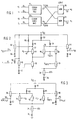
- FIG. 2 An example of an embodiment of an error correcting AND circuit is given in Figure 2 with the two redundant interconnections 10 and 12 providing the wire signals x0 and x1 as inputs.
- the embodiment relies upon a bipolar technology that steers current.
- a current driving transistor 34 is separated from ground by a resistor 36.
- a constant voltage VCS is applied to the base of the current driving transistor 34. Because a bipolar transistor maintains a nearly constant base-emitter current of approximately 0.9V over a wide range of emitter-collector voltages, the voltage at the connection between the resistor 36 and the emitter of the transistor 34 is nearly constant. As a result, a nearly constant emitter-collector current flows through the transistor 34, thus providing a constant current source.
- the size of the resistor 36 is preferably chosen so that this current is approximately 1mA.
- This constant current is switched between a first transistor 38 and a first current steering transistor 39.
- the base of the first transistor 38 is controlled by a signal voltage while the base of the parallel current steering transistor 39 is controlled by a reference voltage V REF2 . If the signal voltage applied to the first transistor 38 is higher than the reference voltage V REF2 , than the first transistor 38 has a lower impedance than the current steering transistor 39 and the constant current mostly flows through the first transistor 38. On the other hand, if this signal voltage is less than the reference voltage V REF2 , then the constant current predominately flows through the current steering transistor 39.
- the first transistor 38 has its base controlled by the emitter output of a first input transistor 40.
- the first input transistor 40 has its collector connected to a positive power supply at a fixed voltage V CC and has its emitter separated from ground by a resistor 42.
- the base of the first input transistor 40 is connected to the redundant interconnection 12 carrying the wire signal x1. If the line signal x1 is high, then the first input transistor 40 conducts so that its emitter becomes high and thus steers the constant current through the first transistor 38. If the wire signal x1, on the other hand, is low, the constant current is steered through the first current steering transistor 39.
- the second input transistor 44 has its collector at a complementary voltage node 52 separated from the power supply voltage V CC by two resistors 48 and 50 and has its base connected to the other redundant line 10 carrying the other wire signal x0.
- the second steering transistor 46 has its collector at a true voltage node 56 separated from the power supply voltage V CC by resistors 50 and 54.
- the exact configuration of the resistors 48, 50 and 54 is not important as long as the resistance in each of the current paths is approximately 800 ohms and separate resistors 48 and 54 are provided. The purpose is to provide 400mV swings, positive and negative, at final output nodes.
- the base of the second steering transistor 46 is connected to another fixed voltage V REF1 .
- the voltage V REF1 is larger than the fixed voltage V REF2 by about 0.9V to compensate for one of the base-emitter voltages of the two transistors 38 and 40.
- a current through the first transistor 38 is steered through the second input transistor 44 when the wire signal x0 is larger than the fixed voltage V REF1 but is steered through the second steering transistor 46 when the wire signal x0 is less than the fixed potential V REF1 .
- Another transistor 48 is connected in the current path from the first steering transistor 39, has its base also controlled by the fixed voltage V REF1 and has its collector connected to the collector of the second steering transistor 46.
- the two wire signals x0 and x1 are being compared against the fixed potentials V REF1 and V REF2 . If both of the wire signals x0 and x1 are high, then the constant current is steered through the resistor 48. On the other hand, if either of the wire signals x0 and x1 are low, then the constant current is steered through the resistor 54. Thus, the voltage at the complementary voltage node 52 at the lower end of the resistor 48 would be low if both of the wire signals x0 and x1 are high while the voltage at the true voltage node 56 at the lower end of the resistor 54 would be high under this condition.
- pull-up resistors 58 and 60 are connected between the bases of the input transistors 40 and 44 and the power supply voltage V CC .
- the pull-up resistor has little effect. If the wire signal x0 is high, there is only a small voltage drop across the pull-up resistor 60. If the wire signal x0 is low, the value of the pull-up resistor 60 has been chosen such that any current flowing through it can be easily driven by the driver of the interconnection 10.
- a preferred value of both pull-up resistors 58 and 60 would be in the range 15 kilohms-20 kilohms.
- the pull-up resistor 58 or 60 pulls the voltage at the respective input transistor 40 or 44 to a high logic level. That is, the pull-up resistors 58 and 60 convert an open fault to a fault that can be treated just like a short to high.
- the AND circuit of Figure 2 together with the pull-up resistors 58 and 60, would correct for one of the redundant interconnections 10 and 12 being open or being shorted to high. However, if the interconnection 10 or 12 is shorted to another interconnection carrying a different signal, the correction is uncertain. The effect of such a short between interconnections would be to, for instance, short together the true voltage node 56 of two different circuits. The likely result would be to drive both of the true voltage nodes to an invalid voltage, intermediate between a valid high and a valid low. That is, what has been described to this point does not provide for a dominant signal state.
- This signal dominance can be provided by the use of emitter-follower outputs, comprising output transistors 62 and 64 having their collectors connected to the power supply voltage V CC and their emitters separated from ground by load resistors 66 and 68.
- the bases of the respective output transistors 62 and 64 are connected to the complementary voltage node 52 and to the true voltage node 56.
- complementary output line 70 carries a complementary output signal x C0
- a true output line 72 carries a true output signal x T0 .
- the signals x CO and x TO on the output lines 70 and 72 should have the previously mentioned 400mV voltage swings.
- the values of the load resistors 66 and 68 are chosen to be much less than the values of the pull-up resistors 58 and 60, for example 500-1000 ohms.
- the use of emitter-follower outputs in the error-correcting AND circuits means that similar faults can be corrected on the output lines 22 and 24. If such faults are considered unimportant, the emitter follower outputs can be dispensed with. It is assumed that any logic function within the logic chip has similar emitter-follower outputs so that inputs to the error-correcting AND circuit have the required state dominance.
- the output transistor 62 is in a high impedance state and the load resistor 66 is in series with a pull-resistor 60 of a different circuit between the power supply voltage V CC and ground.
- the small value of the load resistor 66 prevents a low wire signal x C0 from being pulled to the high logic level.
- Another purpose of the emitter-follower transistor 62 and 64 is to bring the output signals x C0 and x T0 to the normal logic ranges.
- the true output signal x T0 is the corrected signal x CORR of Figure 1.
- the complementary output signal x C0 can be advantageously used if the following logic circuit can use a complementary signal.
- a current driving transistor 74 and associated resistor 76 provides a constant current.
- Two logic transistors 78 and 79 are connected in parallel with their collectors commonly connected through resistors 80 and 81 to the power supply voltage V CC .
- the bases of the logic transistors 78 and 79 are driven respectively by true outputs X TO and Y TO of two error correcting AND circuits
- a current steering transistor 82 effectively provides the fixed voltage V REF1 against which the signals X T0 and Y T0 are compared.
- a resistor 84 is connected in series to the resistor 81.
- Emitter-follower transistors 86 and 88 are separated from ground by respective load resistors 90 and 92, and are controlled by whether the constant current flows through the steering transistor 82 or through one or both of the logic transistors 78 and 79. Both a NOR output 94 and an OR output 96 are provided.
- the emitter-followers provide the proper type of signal dominance for any following error correcting AND circuit.
Landscapes
- Engineering & Computer Science (AREA)
- Physics & Mathematics (AREA)
- Computer Hardware Design (AREA)
- Computing Systems (AREA)
- General Engineering & Computer Science (AREA)
- Mathematical Physics (AREA)
- Power Engineering (AREA)
- Logic Circuits (AREA)
- Hardware Redundancy (AREA)
Claims (7)
- Ein Schaltkreis zur Datenkorrektur mit zwei Datensignal-Eingängen (X0, X1; Y0, Y1) und einem erzeugten Ausgangssignal (Xcorr; Ycorr), wobei der Schaltkreis besteht aus:
- Hilfsmitteln zum Zuführen zweier redundanter Datensignale an die zwei Dateneingänge, wobei diese Hilfsmittel eine Widerstandskopplung (58, 60) an eine Spannungsquelle, die auf einem ersten Potentialwert liegt, beinhalten, die Datensignale sich entweder auf diesem ersten Potentialwert, einem zweiten Potentialwert oder auf einem unbestimmten logischen Zustand befinden und allgemein gilt, daß falls eine Verbindung zwischen zwei signalführenden Datenleitungen mit jeweils verschiedenem Potentialwert auftritt, beide Leitungen dann den ersten Potentialwert führen,- einen Eingangskreis (14; 20) aus der Gruppe der AND und NAND-Schaltungen, welcher die Eingangs-Datensignale (X0, X1; Y0, Y1) aufnimmt, wobei diese Eingangssignale miteinander verglichen werden, so daß ein Ausgangssignal entsteht, welches entsprichta) einem dritten logischen Zustand, falls beide Datensignale auf dem ersten Potentialwert liegen,b) einen vierten logischen Zustand, falls beide Datensignale auf dem zweiten Potentialwert liegen, wobei dieser vierte logische Zustand entweder dem ersten oder dem zweiten logischen Zustand entspricht und komplementär ist zum dritten logischen Zustand,c) dem vierten logischen Zustand, falls beide Datensignale unterschiedliches Potential aufweisen und zwar den ersten und zweiten Potentialwert,d) dem dritten logischen Zustand, falls beide Datensignale unterschiedliches Potential aufweisen und zwar den ersten und den unbestimmten Potentialwert,e) dem vierten logischen Zustand, falls beide Datensignale unterschiedliches Potential aufweisen und zwar den zweiten und den unbestimmten Potentialwert,das Ausgangssignal korrigierten Datensignalen entspricht und
Hilfsmitteln zum Anschluß des Korrekturschaltkreises zwischen zwei Logik-Funktionskreise auf demselben Logik-Chip. - Ein Schaltkreis nach Anspruch 1, welcher zusätzlich einen Ausgangsschaltkreis aufweist, der das Ausgangssignal aufnimmt, um ein verstärktes Signal von entweder dem ersten oder dem zweiten Potentialwert zu erzeugen, wobei dieser Ausgangsschaltkreis Hilfsmittel enthält, um den Ausgangsanschluß auf dem ersten Potentialwert zu halten, falls der Ausgangsanschluß den ersten Potentialwert aufweist und verbunden ist mit einem Ausgangsanschluß eines entsprechenden anderen Ausgangsschaltkreises, welcher den zweiten Potentialwert aufweist.
- Ein Schaltkreis nach Anspruch 1 oder 2, welcher zusätzlich einen Logik-Schaltkreis aufweist, der das Ausgangssignal aufnimmt und zwei äquivalente verstärkte Ausgangssignale an zwei Ausgangsverbindungen erzeugt, wobei dieser logische Schaltkreis zusätzlich zwei Ausgangsschaltkreise beinhaltet, welche den ersten oder zweiten Potentialwert an jeder der Ausgangsverbindungen erzeugen, wobei diese Ausgangsschaltkreise Hilfsmittel enthalten, um jede der Ausgangsverbindungen auf dem ersten Potentialwert zu halten, falls diese Ausgangsverbindung den ersten Potentialwert aufweist und verbunden ist mit einer Ausgangsverbindung eines entsprechenden anderen Ausgangsschaltkreises, welche den zweiten Potentialwert aufweist.
- Ein Schaltkreis nach Anspruch 3, wobei der Logik-Schaltkreis zwei äquivalente Logik-Schaltkreise aufweist, welche jeder einen Ausgangsschaltkreis beinhaltet, der eines der verstärkten Ausgangssignale an einer der Ausgangsverbindungen erzeugt.
- Ein Fehlerkorrektur-Logik-Schaltkreis bestehend aus:
- einer Vielzahl von fehlerkorrigierenden Eingangsschaltkreisen (14, 20), wobei jeder Eingangsschaltkreis zwei Eingangsverbindungen (10, 12; 16, 18) aufnimmt, welche zwei entsprechende Signale führen (X0, X1; Y0, Y1), die einen ersten oder zweiten logischen Zustand repräsentieren, wobei ein Signal einen ersten, einen zweiten oder einen unbestimmten Potentialwert aufweist und der Eingangsschaltkreis ein korrigiertes Signal erzeugt, welches entsprichta) einem dritten logischen Zustand, falls beide Datensignale auf dem ersten Potentialwert liegen,b) einen vierten logischen Zustand, falls beide Datensignale auf dem zweiten Potentialwert liegen, wobei dieser vierte logische Zustand entweder dem ersten oder dem zweiten logischen Zustand entspricht und komplementär ist zum dritten logischen Zustand,c) dem vierten logischen Zustand, falls beide Datensignale unterschiedliches Potential aufweisen und zwar den ersten und zweiten Potentialwert,d) dem dritten logischen Zustand, falls beide Datensignale unterschiedliches Potential aufweisen und zwar den ersten und den unbestimmten Potentialwert,e) dem vierten logischen Zustand, falls beide Datensignale unterschiedliches Potential aufweisen und zwar den zweiten und den unbestimmten Potentialwert,- zwei äquivalenten Logik-Schaltkreisen, die jeder das korrigierte Signal von den zahlreichen Eingangsschaltkreisen empfangen und nach einer vorgegebenen logischen Funktion ein Ausgangssignal an einer entsprechenden Ausgangsverbindung erzeugen, wobei jeder der äquivalenten Schaltkreise einen Ausgangsschaltkreis aufweist, der den ersten oder zweiten Potentialwert an der Ausgangsverbindung erzeugt, wobei der Ausgangsschaltkreis Hilfsmittel beinhaltet, um jede der Ausgangsverbindungen auf dem ersten Potentialwert zu halten, falls eine Ausgangsverbindung den ersten Potentialwert führt und verbunden ist mit einer anderen Ausgangsverbindung eines entsprechenden Ausgangsschaltkreises, welche den zweiten Potentialwert führt, wobei die zwei Ausgangsverbindungen der zwei äquivalenten Logik-Schaltkreise angeschlossen sind an Eingangsverbindungen von anderen Fehlerkorrektur-Logik-Schaltkreisen. - Ein Fehlerkorrektur-Logik-Schaltkreis entsprechend einem der Ansprüche 2 bis 5, wobei die Ausgangsschaltkreise eine Widerstandskopplung an eine Spannungsquelle auf dem Potential des zweiten Potentialwerts beinhalten.
- Ein Fehlerkorrektur-Logik-Schaltkreis entsprechend einem der Ansprüche 2 bis 6, wobei die Ausgangsschaltkreise aus einem Emitter-Folger-Kreis bestehen.
Applications Claiming Priority (2)
| Application Number | Priority Date | Filing Date | Title |
|---|---|---|---|
| US792097 | 1985-10-28 | ||
| US06/792,097 US4719629A (en) | 1985-10-28 | 1985-10-28 | Dual fault-masking redundancy logic circuits |
Publications (3)
| Publication Number | Publication Date |
|---|---|
| EP0220596A2 EP0220596A2 (de) | 1987-05-06 |
| EP0220596A3 EP0220596A3 (en) | 1988-11-30 |
| EP0220596B1 true EP0220596B1 (de) | 1992-01-02 |
Family
ID=25155779
Family Applications (1)
| Application Number | Title | Priority Date | Filing Date |
|---|---|---|---|
| EP86114202A Expired - Lifetime EP0220596B1 (de) | 1985-10-28 | 1986-10-14 | Doppelredundante fehlermaskierende logische Schaltungen |
Country Status (4)
| Country | Link |
|---|---|
| US (1) | US4719629A (de) |
| EP (1) | EP0220596B1 (de) |
| JP (1) | JPH061897B2 (de) |
| DE (1) | DE3683242D1 (de) |
Families Citing this family (11)
| Publication number | Priority date | Publication date | Assignee | Title |
|---|---|---|---|---|
| US4829198A (en) * | 1987-04-10 | 1989-05-09 | International Business Machines Corporation | Fault tolerant logical circuitry |
| JPS63318816A (ja) * | 1987-06-12 | 1988-12-27 | インターナシヨナル・ビジネス・マシーンズ・コーポレーシヨン | 欠陥許容性を有する論理回路 |
| US5187711A (en) * | 1988-09-20 | 1993-02-16 | Fujitsu Limited | Error correction method for multicarrier radio transmission system |
| US5260952A (en) * | 1991-04-30 | 1993-11-09 | Ibm Corporation | Fault tolerant logic system |
| US5347184A (en) * | 1992-12-29 | 1994-09-13 | Texas Instruments Incorporated | Dual receiver edge-triggered digital signal level detection system |
| US5528165A (en) * | 1995-04-03 | 1996-06-18 | Sun Microsystems, Inc. | Logic signal validity verification apparatus |
| US6035416A (en) * | 1997-10-15 | 2000-03-07 | International Business Machines Corp. | Method and apparatus for interface dual modular redundancy |
| CN1303532C (zh) * | 2003-07-10 | 2007-03-07 | 浙江中控技术有限公司 | 冗余切换控制方法及电路 |
| US20090220802A1 (en) * | 2006-02-21 | 2009-09-03 | Von Ardenne Anlagentechnik Gmbh | Highly reflective layer system, method for producing the layer system and device for carrying out the method |
| US8146028B1 (en) | 2008-11-19 | 2012-03-27 | Xilinx, Inc. | Duplicate design flow for mitigation of soft errors in IC operation |
| CN110971228B (zh) * | 2019-12-04 | 2022-08-02 | 成都锐成芯微科技股份有限公司 | 一种高速时钟驱动电路 |
Family Cites Families (9)
| Publication number | Priority date | Publication date | Assignee | Title |
|---|---|---|---|---|
| US3305735A (en) * | 1963-10-07 | 1967-02-21 | Bendix Corp | Signal selection and monitoring system utilizing redundant voting circuits |
| US3524073A (en) * | 1965-10-18 | 1970-08-11 | Martin Marietta Corp | Redundant majority voter |
| US3558905A (en) * | 1967-05-02 | 1971-01-26 | Kokusai Denshin Denwa Co Ltd | Fail-safe logical system |
| US3800164A (en) * | 1969-01-02 | 1974-03-26 | Us Navy | Redundant logic circuit |
| US3859513A (en) * | 1973-02-28 | 1975-01-07 | Univ Washington | Switching and digital system |
| US4342112A (en) * | 1980-09-08 | 1982-07-27 | Rockwell International Corporation | Error checking circuit |
| JPS58225448A (ja) * | 1982-06-23 | 1983-12-27 | Mitsubishi Electric Corp | シ−ケンス制御装置 |
| JPS6016729A (ja) * | 1983-03-18 | 1985-01-28 | Nec Corp | 論理回路 |
| US4617475A (en) * | 1984-03-30 | 1986-10-14 | Trilogy Computer Development Partners, Ltd. | Wired logic voting circuit |
-
1985
- 1985-10-28 US US06/792,097 patent/US4719629A/en not_active Expired - Fee Related
-
1986
- 1986-08-20 JP JP61193026A patent/JPH061897B2/ja not_active Expired - Lifetime
- 1986-10-14 EP EP86114202A patent/EP0220596B1/de not_active Expired - Lifetime
- 1986-10-14 DE DE8686114202T patent/DE3683242D1/de not_active Expired - Lifetime
Non-Patent Citations (1)
| Title |
|---|
| Valvo Schaltungssammlung, Heft 2, VALVO GmbH, Hamburg, June 1972, No. 116,117 * |
Also Published As
| Publication number | Publication date |
|---|---|
| EP0220596A3 (en) | 1988-11-30 |
| JPS62102336A (ja) | 1987-05-12 |
| JPH061897B2 (ja) | 1994-01-05 |
| EP0220596A2 (de) | 1987-05-06 |
| DE3683242D1 (de) | 1992-02-13 |
| US4719629A (en) | 1988-01-12 |
Similar Documents
| Publication | Publication Date | Title |
|---|---|---|
| US4617475A (en) | Wired logic voting circuit | |
| EP0220596B1 (de) | Doppelredundante fehlermaskierende logische Schaltungen | |
| US5374861A (en) | Differential termination network for differential transmitters and receivers | |
| US4621201A (en) | Integrated circuit redundancy and method for achieving high-yield production | |
| JPH03506089A (ja) | 二進信号を多数決選択する論理回路網に潜在する誤りを除去する方法 | |
| CA1278349C (en) | Fault tolerant logical circuitry | |
| GB1586140A (en) | Logic circuits incorporating a dual function input | |
| JPS58197921A (ja) | 論理素子 | |
| EP0216756B1 (de) | Integrierte schaltungsvorrichtung, die eingangssignale annimmt und ausgangssignale erzeugt auf den höhen verschiedener logischer scharen | |
| US4250407A (en) | Multi function patch pin circuit | |
| US3628000A (en) | Data handling devices for radix {37 n{30 2{38 {0 operation | |
| EP0114320A2 (de) | Offsetspannungsschaltung zur Anwendung mit einem Leitungsempfänger oder dergleichen | |
| US4682058A (en) | Three-state logic circuit for wire-ORing to a data bus | |
| US4709166A (en) | Complementary cascoded logic circuit | |
| EP0144218B1 (de) | EC-Torfeld | |
| EP0075079A1 (de) | Schaltungsnetzwerkkontrollsystem | |
| US20080143374A1 (en) | ANTI-SEE PROTECTION TECHNIQUES FOR HIGH-SPEED ICs WITH A CURRENT-SWITCHING ARCHITECTURE | |
| US6240139B1 (en) | Apparatus and method for repeating simultaneously transmitted signals on a single transmission path | |
| US4888499A (en) | Three input exclusive OR-NOR gate circuit | |
| US4054803A (en) | Matcher circuit | |
| JP3664820B2 (ja) | 伝送装置間インタフェースにおけるフェイルセーフ回路 | |
| US6130812A (en) | Protection circuit for high speed communication | |
| EP0294602A2 (de) | Fehlertolerante logische Schaltung | |
| JPS6028325A (ja) | 論理回路 | |
| JPS60211548A (ja) | 切替制御回路 |
Legal Events
| Date | Code | Title | Description |
|---|---|---|---|
| PUAI | Public reference made under article 153(3) epc to a published international application that has entered the european phase |
Free format text: ORIGINAL CODE: 0009012 |
|
| AK | Designated contracting states |
Kind code of ref document: A2 Designated state(s): DE FR GB IT |
|
| 17P | Request for examination filed |
Effective date: 19870821 |
|
| PUAL | Search report despatched |
Free format text: ORIGINAL CODE: 0009013 |
|
| AK | Designated contracting states |
Kind code of ref document: A3 Designated state(s): DE FR GB IT |
|
| 17Q | First examination report despatched |
Effective date: 19891116 |
|
| GRAA | (expected) grant |
Free format text: ORIGINAL CODE: 0009210 |
|
| AK | Designated contracting states |
Kind code of ref document: B1 Designated state(s): DE FR GB IT |
|
| PG25 | Lapsed in a contracting state [announced via postgrant information from national office to epo] |
Ref country code: IT Free format text: LAPSE BECAUSE OF FAILURE TO SUBMIT A TRANSLATION OF THE DESCRIPTION OR TO PAY THE FEE WITHIN THE PRESCRIBED TIME-LIMIT;WARNING: LAPSES OF ITALIAN PATENTS WITH EFFECTIVE DATE BEFORE 2007 MAY HAVE OCCURRED AT ANY TIME BEFORE 2007. THE CORRECT EFFECTIVE DATE MAY BE DIFFERENT FROM THE ONE RECORDED. Effective date: 19920102 |
|
| REF | Corresponds to: |
Ref document number: 3683242 Country of ref document: DE Date of ref document: 19920213 |
|
| ET | Fr: translation filed | ||
| PG25 | Lapsed in a contracting state [announced via postgrant information from national office to epo] |
Ref country code: GB Effective date: 19921014 |
|
| PLBE | No opposition filed within time limit |
Free format text: ORIGINAL CODE: 0009261 |
|
| STAA | Information on the status of an ep patent application or granted ep patent |
Free format text: STATUS: NO OPPOSITION FILED WITHIN TIME LIMIT |
|
| 26N | No opposition filed | ||
| GBPC | Gb: european patent ceased through non-payment of renewal fee |
Effective date: 19921014 |
|
| PG25 | Lapsed in a contracting state [announced via postgrant information from national office to epo] |
Ref country code: FR Effective date: 19930630 |
|
| PG25 | Lapsed in a contracting state [announced via postgrant information from national office to epo] |
Ref country code: DE Effective date: 19930701 |
|
| REG | Reference to a national code |
Ref country code: FR Ref legal event code: ST |