EP0220596B1 - Dual fault-masking redundancy logic circuits - Google Patents
Dual fault-masking redundancy logic circuits Download PDFInfo
- Publication number
- EP0220596B1 EP0220596B1 EP86114202A EP86114202A EP0220596B1 EP 0220596 B1 EP0220596 B1 EP 0220596B1 EP 86114202 A EP86114202 A EP 86114202A EP 86114202 A EP86114202 A EP 86114202A EP 0220596 B1 EP0220596 B1 EP 0220596B1
- Authority
- EP
- European Patent Office
- Prior art keywords
- logic
- output
- state
- circuit
- potential
- Prior art date
- Legal status (The legal status is an assumption and is not a legal conclusion. Google has not performed a legal analysis and makes no representation as to the accuracy of the status listed.)
- Expired - Lifetime
Links
Images
Classifications
-
- H—ELECTRICITY
- H03—ELECTRONIC CIRCUITRY
- H03K—PULSE TECHNIQUE
- H03K19/00—Logic circuits, i.e. having at least two inputs acting on one output; Inverting circuits
- H03K19/02—Logic circuits, i.e. having at least two inputs acting on one output; Inverting circuits using specified components
- H03K19/08—Logic circuits, i.e. having at least two inputs acting on one output; Inverting circuits using specified components using semiconductor devices
- H03K19/082—Logic circuits, i.e. having at least two inputs acting on one output; Inverting circuits using specified components using semiconductor devices using bipolar transistors
- H03K19/086—Emitter coupled logic
- H03K19/0866—Stacked emitter coupled logic
-
- H—ELECTRICITY
- H03—ELECTRONIC CIRCUITRY
- H03K—PULSE TECHNIQUE
- H03K19/00—Logic circuits, i.e. having at least two inputs acting on one output; Inverting circuits
- H03K19/003—Modifications for increasing the reliability for protection
- H03K19/00392—Modifications for increasing the reliability for protection by circuit redundancy
-
- H—ELECTRICITY
- H03—ELECTRONIC CIRCUITRY
- H03K—PULSE TECHNIQUE
- H03K19/00—Logic circuits, i.e. having at least two inputs acting on one output; Inverting circuits
- H03K19/02—Logic circuits, i.e. having at least two inputs acting on one output; Inverting circuits using specified components
- H03K19/08—Logic circuits, i.e. having at least two inputs acting on one output; Inverting circuits using specified components using semiconductor devices
- H03K19/082—Logic circuits, i.e. having at least two inputs acting on one output; Inverting circuits using specified components using semiconductor devices using bipolar transistors
- H03K19/086—Emitter coupled logic
-
- H—ELECTRICITY
- H03—ELECTRONIC CIRCUITRY
- H03K—PULSE TECHNIQUE
- H03K19/00—Logic circuits, i.e. having at least two inputs acting on one output; Inverting circuits
- H03K19/02—Logic circuits, i.e. having at least two inputs acting on one output; Inverting circuits using specified components
- H03K19/173—Logic circuits, i.e. having at least two inputs acting on one output; Inverting circuits using specified components using elementary logic circuits as components
- H03K19/1733—Controllable logic circuits
- H03K19/1738—Controllable logic circuits using cascode switch logic [CSL] or cascode emitter coupled logic [CECL]
Definitions
- the invention relates generally to logic circuits.
- the invention relates to a logic circuit design which masks two classes of faults by the use of redundant circuits and interconnects.
- a third common failure mode is where the metal interconnection shorts to a fixed potential, usually a high potential. This failure mode is particularly important when a substrate etch or reactive ion etching is used to obtain fine metal interconnections.
- TMR triple modular redundancy
- Tripling the number of interconnections would, of course, require tripling the amount of chip area devoted to the long interconnections. It may be better to, instead, use a single interconnection of lower density to achieve an acceptable reliability without TMR.
- the area problem becomes even more severe if the triple modular redundancy is extended to include the logic function that the interconnections are driving. Take the example of a two-input logic function, with each input being driven by a long interconnection.
- TMR design there are two sets of three redundant lines. The two sets of three lines are combined in all possible combinations in separate logic circuits and the vote is performed on the output of the logic circuit.
- this approach requires that there be nine logic circuits. Needless to say, this entails a very heavy price in chip area.
- the error correcting AND circuits 14 and 20 mask at least some of the faults on the redundant signal lines 10 and 12 or 16 and 18 that they receive and produce corrected signals x CORR or y CORR on their respective outputs 22 and 24.
- the output lines 22 and 24 are led to both of two redundant logic functions, here represented by NOR circuits 26 and 28 that produce redundant logic outputs w0 and w1 on their respective outputs 30 and 32.
- the redundant output lines 30 and 32 are led to other logic circuits to be used as inputs, similarly to the redundant lines 10 and 12 for the signals x0 and x1.
- the invention can correct a single fault on the redundant input lines 10 and 12 and possibly another single fault on the input lines 16 and 18.
- the redundancy of the logic blocks 26 and 28 prevents a fault on one of the output lines 30 and 32 from propagating to the other of the output lines 30 and 32.
- dual buffer amplifiers connected to a single output would accomplish the same isolation.
- the dual logic blocks 26 and 28 provide further fault redundancy within the logic blocks themselves.
- logic function represented in Figure 1 is a two-input NOR
- other logic functions can be similarly accomplished such as a higher order NOR, an OR, an AND or a NOR function. These alternative embodiments would substitute the desired function for each of the logic blocks 26 and 28. If there are additional input variables, then additional error correcting AND circuits would be required. On the other hand, a single error correcting AND circuit 14 can be used if only a single logic signal x is considered to be subject to faults.
- the characteristics of the error correcting AND circuit is, of course, crucial to the invention.
- a normal AND circuit would correct only a limited number of fault types. It would correct any line signal which was spuriously high but would fail to correct a fault signal that was spuriously low.
- An open interconnection has a floating potential and thus can be either high or low regardless of the driving signal.
- a conventional AND circuit would not be able to correct this open situation.
- One embodiment of the error correcting AND circuit corrects three types of faults on either one of the two input lines 10 and 12. Namely, these faults are a short to a high signal, a short to a wrong state of another signal and an open. A short to a wrong state of another signal depends upon the characteristics of the logic technology. This characteristic requires that when two separated lines are shorted together, then the resultant signal is high if either of the signals on the two lines is high. Of course, the invention can be easily modified to accommodate the low signal being the dominant signal and shorts to a low state.
- the desired truth table for the error correcting AND circuits 14 and 16 are given in Table 1. TABLE 1 X0 X1 X CORR Comments H H H All correct L L L All correct H L L x0 shorted to H OPEN H H x0 open OPEN L L x0 open
- the first two rows represent the situation where both of the redundant input lines carry the correct signals x0 and x1. It should, however, be noted that the correct signal may, in fact, be due to a fault. That is, if the correct logic signal is high but the input line for x0 is shorted high, nonetheless, the wire signal x0 is correct.
- the third line represents the case when one of the input lines is shorted high while the other input line carries a correct low signal. In this case, the error correcting AND circuit produces a low.
- the last two lines represent the case when one of the input lines is open but the error correcting AND circuit nonetheless produces the correct output signal x CORR .
- the truth table of Table 1 represents the fault occurring to the line signal x0 but it should be understood that similar results are obtained when the short or the open fault occurs to the wire signal x1.
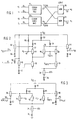
- FIG. 2 An example of an embodiment of an error correcting AND circuit is given in Figure 2 with the two redundant interconnections 10 and 12 providing the wire signals x0 and x1 as inputs.
- the embodiment relies upon a bipolar technology that steers current.
- a current driving transistor 34 is separated from ground by a resistor 36.
- a constant voltage VCS is applied to the base of the current driving transistor 34. Because a bipolar transistor maintains a nearly constant base-emitter current of approximately 0.9V over a wide range of emitter-collector voltages, the voltage at the connection between the resistor 36 and the emitter of the transistor 34 is nearly constant. As a result, a nearly constant emitter-collector current flows through the transistor 34, thus providing a constant current source.
- the size of the resistor 36 is preferably chosen so that this current is approximately 1mA.
- This constant current is switched between a first transistor 38 and a first current steering transistor 39.
- the base of the first transistor 38 is controlled by a signal voltage while the base of the parallel current steering transistor 39 is controlled by a reference voltage V REF2 . If the signal voltage applied to the first transistor 38 is higher than the reference voltage V REF2 , than the first transistor 38 has a lower impedance than the current steering transistor 39 and the constant current mostly flows through the first transistor 38. On the other hand, if this signal voltage is less than the reference voltage V REF2 , then the constant current predominately flows through the current steering transistor 39.
- the first transistor 38 has its base controlled by the emitter output of a first input transistor 40.
- the first input transistor 40 has its collector connected to a positive power supply at a fixed voltage V CC and has its emitter separated from ground by a resistor 42.
- the base of the first input transistor 40 is connected to the redundant interconnection 12 carrying the wire signal x1. If the line signal x1 is high, then the first input transistor 40 conducts so that its emitter becomes high and thus steers the constant current through the first transistor 38. If the wire signal x1, on the other hand, is low, the constant current is steered through the first current steering transistor 39.
- the second input transistor 44 has its collector at a complementary voltage node 52 separated from the power supply voltage V CC by two resistors 48 and 50 and has its base connected to the other redundant line 10 carrying the other wire signal x0.
- the second steering transistor 46 has its collector at a true voltage node 56 separated from the power supply voltage V CC by resistors 50 and 54.
- the exact configuration of the resistors 48, 50 and 54 is not important as long as the resistance in each of the current paths is approximately 800 ohms and separate resistors 48 and 54 are provided. The purpose is to provide 400mV swings, positive and negative, at final output nodes.
- the base of the second steering transistor 46 is connected to another fixed voltage V REF1 .
- the voltage V REF1 is larger than the fixed voltage V REF2 by about 0.9V to compensate for one of the base-emitter voltages of the two transistors 38 and 40.
- a current through the first transistor 38 is steered through the second input transistor 44 when the wire signal x0 is larger than the fixed voltage V REF1 but is steered through the second steering transistor 46 when the wire signal x0 is less than the fixed potential V REF1 .
- Another transistor 48 is connected in the current path from the first steering transistor 39, has its base also controlled by the fixed voltage V REF1 and has its collector connected to the collector of the second steering transistor 46.
- the two wire signals x0 and x1 are being compared against the fixed potentials V REF1 and V REF2 . If both of the wire signals x0 and x1 are high, then the constant current is steered through the resistor 48. On the other hand, if either of the wire signals x0 and x1 are low, then the constant current is steered through the resistor 54. Thus, the voltage at the complementary voltage node 52 at the lower end of the resistor 48 would be low if both of the wire signals x0 and x1 are high while the voltage at the true voltage node 56 at the lower end of the resistor 54 would be high under this condition.
- pull-up resistors 58 and 60 are connected between the bases of the input transistors 40 and 44 and the power supply voltage V CC .
- the pull-up resistor has little effect. If the wire signal x0 is high, there is only a small voltage drop across the pull-up resistor 60. If the wire signal x0 is low, the value of the pull-up resistor 60 has been chosen such that any current flowing through it can be easily driven by the driver of the interconnection 10.
- a preferred value of both pull-up resistors 58 and 60 would be in the range 15 kilohms-20 kilohms.
- the pull-up resistor 58 or 60 pulls the voltage at the respective input transistor 40 or 44 to a high logic level. That is, the pull-up resistors 58 and 60 convert an open fault to a fault that can be treated just like a short to high.
- the AND circuit of Figure 2 together with the pull-up resistors 58 and 60, would correct for one of the redundant interconnections 10 and 12 being open or being shorted to high. However, if the interconnection 10 or 12 is shorted to another interconnection carrying a different signal, the correction is uncertain. The effect of such a short between interconnections would be to, for instance, short together the true voltage node 56 of two different circuits. The likely result would be to drive both of the true voltage nodes to an invalid voltage, intermediate between a valid high and a valid low. That is, what has been described to this point does not provide for a dominant signal state.
- This signal dominance can be provided by the use of emitter-follower outputs, comprising output transistors 62 and 64 having their collectors connected to the power supply voltage V CC and their emitters separated from ground by load resistors 66 and 68.
- the bases of the respective output transistors 62 and 64 are connected to the complementary voltage node 52 and to the true voltage node 56.
- complementary output line 70 carries a complementary output signal x C0
- a true output line 72 carries a true output signal x T0 .
- the signals x CO and x TO on the output lines 70 and 72 should have the previously mentioned 400mV voltage swings.
- the values of the load resistors 66 and 68 are chosen to be much less than the values of the pull-up resistors 58 and 60, for example 500-1000 ohms.
- the use of emitter-follower outputs in the error-correcting AND circuits means that similar faults can be corrected on the output lines 22 and 24. If such faults are considered unimportant, the emitter follower outputs can be dispensed with. It is assumed that any logic function within the logic chip has similar emitter-follower outputs so that inputs to the error-correcting AND circuit have the required state dominance.
- the output transistor 62 is in a high impedance state and the load resistor 66 is in series with a pull-resistor 60 of a different circuit between the power supply voltage V CC and ground.
- the small value of the load resistor 66 prevents a low wire signal x C0 from being pulled to the high logic level.
- Another purpose of the emitter-follower transistor 62 and 64 is to bring the output signals x C0 and x T0 to the normal logic ranges.
- the true output signal x T0 is the corrected signal x CORR of Figure 1.
- the complementary output signal x C0 can be advantageously used if the following logic circuit can use a complementary signal.
- a current driving transistor 74 and associated resistor 76 provides a constant current.
- Two logic transistors 78 and 79 are connected in parallel with their collectors commonly connected through resistors 80 and 81 to the power supply voltage V CC .
- the bases of the logic transistors 78 and 79 are driven respectively by true outputs X TO and Y TO of two error correcting AND circuits
- a current steering transistor 82 effectively provides the fixed voltage V REF1 against which the signals X T0 and Y T0 are compared.
- a resistor 84 is connected in series to the resistor 81.
- Emitter-follower transistors 86 and 88 are separated from ground by respective load resistors 90 and 92, and are controlled by whether the constant current flows through the steering transistor 82 or through one or both of the logic transistors 78 and 79. Both a NOR output 94 and an OR output 96 are provided.
- the emitter-followers provide the proper type of signal dominance for any following error correcting AND circuit.
Description
- The invention relates generally to logic circuits. In particular, the invention relates to a logic circuit design which masks two classes of faults by the use of redundant circuits and interconnects.
- As integrated circuits for logic become ever larger and more complex, usually as a result of further minaturization of individual elements, it has become increasingly difficult to produce perfectly operating logic circuits at an acceptable yield. As the dimensions for the electrical components on the integrated chip have become ever smaller, the processing margins have decreased. In the past, the margins were sufficiently large that an acceptable yield of perfect chips has been obtained. This acceptable yield is becoming increasingly difficult to obtain. Furthermore, noise margins have been correspondingly decreasing. That is, logic chip may operate satisfactorily a majority of the time but occasionally a noise transient is randomly impressed upon one of the internal lines and an incorrect logic operation results.
- As a result, increasing attention has been devoted to error correcting logic, both for the hard failures of the exceeded processing margins and for the soft failures of the transient noise failures.
- It is believed that a large fraction of failures are associated, not with the logic functions themselves, but instead with the interconnections between separated active devices. Internal logic signals often need to be conveyed relatively long distances. If there are a large number of such internal logic signal interconnections, the chip designer attempts to make the interconnection pathways as dense as possible. That is, the interconnections, typically of metal, are made relatively narrow and are separated from neighboring interconnections by minimum distances. There are several dominant failure modes for these interconnections. An interconnection can become separated somewhere in the middle so that the input to the following logic stage sees an open circuit, that is, a floating potential. Another common failure mode is that two neighboring interconnections are shorted together. In many types of logic, when two wires carrying different signals are shorted together, one logic level will dominate over the other. Thus, in the only significant logic combination in this failure mode in which one wire carries a high logic signal and the other carries a low logic signal, a short will produce a predetermined logic signal, for instance a high logic signal in many important technologies. A third common failure mode is where the metal interconnection shorts to a fixed potential, usually a high potential. This failure mode is particularly important when a substrate etch or reactive ion etching is used to obtain fine metal interconnections.
- One technique for masking faults is the use of a triple modular redundancy (TMR). Applying TMR to interconnection faults will require that each interconnection be replaced by three interconnections. Then, at the input to logic block, there would be an error correcting input stage. This error correcting input stage would compare the signals on all three of the interconnections and use as an error corrected output whatever signal is indicated on at least two of the interconnections. That is, there would be a vote between the three redundant wires. In triple modular redundancy there is the assumption that there is only a single fault so that only a single error can be corrected. This single error assumption is common in most error correcting techniques. Triple modular redundancy, although very effective, entails a substantial trade-off in chip design. Tripling the number of interconnections would, of course, require tripling the amount of chip area devoted to the long interconnections. It may be better to, instead, use a single interconnection of lower density to achieve an acceptable reliability without TMR. The area problem becomes even more severe if the triple modular redundancy is extended to include the logic function that the interconnections are driving. Take the example of a two-input logic function, with each input being driven by a long interconnection. For a combined TMR design, there are two sets of three redundant lines. The two sets of three lines are combined in all possible combinations in separate logic circuits and the vote is performed on the output of the logic circuit. However, this approach requires that there be nine logic circuits. Needless to say, this entails a very heavy price in chip area.
- Another fault masking method is described in "Valvo Schaltungssammlung", Heft 2, Valvo GmbH, Hamburg, June 1972, No. 116, 117. This document relates to an error correction circuit designed for suppressing disturbances occuring during binary signal transmission using two redundant signal lines. Only distortions which produce an identical potential on both input data lines are corrected and only as far as they were significantly shorter than usual potential changes during normal data flow. Thus only specific types of faulty input signals are suppressed by this circuit.
- The invention as claimed is intended to remedy these drawbacks.
- One way of carrying out the invention is described in detail below with reference to drawings which illustrate only one specific embodiment, in which:
- Figure 1 is a block diagram of an embodiment of an error correction logic stage.
- Figure 2 is a circuit diagram of the error-correcting AND circuit of Figure 1.
- Figure 3 is a circuit diagram of the NOR logic of Figure 1.
- By means of the invention, dual redundant interconnections and error correcting inputs correct many classes of failure. Thus for a logic signal x, there would be two interconnecting wires carrying wire signals xo and x₁. For logic signal y, there would be two wire signals yo and y₁. A relatively simple error corrected logic circuit is shown in Figure 1 for a NOR function that is, the output w = NOR (x, y). Each of two
redundant interconnecting wires circuit 14. Similarly,redundant interconnecting wires circuit 20. The error correcting ANDcircuits redundant signal lines respective outputs output lines NOR circuits respective outputs 30 and 32. Theredundant output lines 30 and 32 are led to other logic circuits to be used as inputs, similarly to theredundant lines - The invention can correct a single fault on the
redundant input lines input lines logic blocks output lines 30 and 32 from propagating to the other of theoutput lines 30 and 32. Of course, dual buffer amplifiers connected to a single output would accomplish the same isolation. However, thedual logic blocks - Although the logic function represented in Figure 1 is a two-input NOR, other logic functions can be similarly accomplished such as a higher order NOR, an OR, an AND or a NOR function. These alternative embodiments would substitute the desired function for each of the
logic blocks circuit 14 can be used if only a single logic signal x is considered to be subject to faults. - The characteristics of the error correcting AND circuit is, of course, crucial to the invention. A normal AND circuit would correct only a limited number of fault types. It would correct any line signal which was spuriously high but would fail to correct a fault signal that was spuriously low. An open interconnection has a floating potential and thus can be either high or low regardless of the driving signal. A conventional AND circuit would not be able to correct this open situation.
- One embodiment of the error correcting AND circuit corrects three types of faults on either one of the two
input lines circuits TABLE 1 X₀ X₁ XCORR Comments H H H All correct L L L All correct H L L x₀ shorted to H OPEN H H x₀ open OPEN L L x₀ open - In the truth table of Table 1, the first two rows represent the situation where both of the redundant input lines carry the correct signals x₀ and x₁. It should, however, be noted that the correct signal may, in fact, be due to a fault. That is, if the correct logic signal is high but the input line for x₀ is shorted high, nonetheless, the wire signal x₀ is correct. The third line represents the case when one of the input lines is shorted high while the other input line carries a correct low signal. In this case, the error correcting AND circuit produces a low. The last two lines represent the case when one of the input lines is open but the error correcting AND circuit nonetheless produces the correct output signal xCORR. The truth table of Table 1 represents the fault occurring to the line signal x₀ but it should be understood that similar results are obtained when the short or the open fault occurs to the wire signal x₁.
- An example of an embodiment of an error correcting AND circuit is given in Figure 2 with the two
redundant interconnections current driving transistor 34 is separated from ground by aresistor 36. A constant voltage VCS is applied to the base of thecurrent driving transistor 34. Because a bipolar transistor maintains a nearly constant base-emitter current of approximately 0.9V over a wide range of emitter-collector voltages, the voltage at the connection between theresistor 36 and the emitter of thetransistor 34 is nearly constant. As a result, a nearly constant emitter-collector current flows through thetransistor 34, thus providing a constant current source. The size of theresistor 36 is preferably chosen so that this current is approximately 1mA. This constant current is switched between afirst transistor 38 and a firstcurrent steering transistor 39. The base of thefirst transistor 38 is controlled by a signal voltage while the base of the parallelcurrent steering transistor 39 is controlled by a reference voltage VREF2. If the signal voltage applied to thefirst transistor 38 is higher than the reference voltage VREF2, than thefirst transistor 38 has a lower impedance than thecurrent steering transistor 39 and the constant current mostly flows through thefirst transistor 38. On the other hand, if this signal voltage is less than the reference voltage VREF2, then the constant current predominately flows through thecurrent steering transistor 39. - The
first transistor 38 has its base controlled by the emitter output of afirst input transistor 40. Thefirst input transistor 40 has its collector connected to a positive power supply at a fixed voltage VCC and has its emitter separated from ground by aresistor 42. The base of thefirst input transistor 40 is connected to theredundant interconnection 12 carrying the wire signal x₁. If the line signal x₁ is high, then thefirst input transistor 40 conducts so that its emitter becomes high and thus steers the constant current through thefirst transistor 38. If the wire signal x₁, on the other hand, is low, the constant current is steered through the firstcurrent steering transistor 39. - If the constant current is steered through the
first transistor 38, then current steering is again performed between asecond input transistor 44 and a secondcurrent steering transistor 46. Thesecond input transistor 44 has its collector at acomplementary voltage node 52 separated from the power supply voltage VCC by tworesistors redundant line 10 carrying the other wire signal x₀. Thesecond steering transistor 46 has its collector at atrue voltage node 56 separated from the power supply voltage VCC byresistors resistors separate resistors second steering transistor 46 is connected to another fixed voltage VREF1. The voltage VREF1 is larger than the fixed voltage VREF2 by about 0.9V to compensate for one of the base-emitter voltages of the twotransistors - By a current switching operation similar to that previously described, a current through the
first transistor 38 is steered through thesecond input transistor 44 when the wire signal x₀ is larger than the fixed voltage VREF1 but is steered through thesecond steering transistor 46 when the wire signal x₀ is less than the fixed potential VREF1. Anothertransistor 48 is connected in the current path from thefirst steering transistor 39, has its base also controlled by the fixed voltage VREF1 and has its collector connected to the collector of thesecond steering transistor 46. - Thus, the two wire signals x₀ and x₁ are being compared against the fixed potentials VREF1 and VREF2. If both of the wire signals x₀ and x₁ are high, then the constant current is steered through the
resistor 48. On the other hand, if either of the wire signals x₀ and x₁ are low, then the constant current is steered through theresistor 54. Thus, the voltage at thecomplementary voltage node 52 at the lower end of theresistor 48 would be low if both of the wire signals x₀ and x₁ are high while the voltage at thetrue voltage node 56 at the lower end of theresistor 54 would be high under this condition. On the other hand, if either of the wire signals x₀ and x₁ is low, then the voltage at thecomplementary voltage node 52 is high and the voltage at thetrue voltage node 56 is low. That is, the signal at the truevoltage node node 56 represents the logical function AND (x₀, x₁) and the voltage at thecomplementary voltage node 52 represents the function NAND(x₀, x₁). - What has been described to this point is a fairly routine AND/HAND circuit. Indeed, the circuit of Fig. 1 would be functionally similar to the AND and NOR circuits disclosed by Yu et al. in U.S. Patent 3,539,824 if the error correcting context is ignored. As mentioned previously, an AND circuit corrects many types of faults associated with shorted
interconnections redundant interconnections - In order to provide for the full correction of one of the
interconnections resistors input transistors resistors 60, if theinterconnection 10 is being driven by a valid wire signal x₀, the pull-up resistor has little effect. If the wire signal x₀ is high, there is only a small voltage drop across the pull-upresistor 60. If the wire signal x₀ is low, the value of the pull-upresistor 60 has been chosen such that any current flowing through it can be easily driven by the driver of theinterconnection 10. A preferred value of both pull-upresistors - On the other hand, if one of the
interconnections interconnection resistor respective input transistor resistors - The AND circuit of Figure 2, together with the pull-up
resistors redundant interconnections interconnection true voltage node 56 of two different circuits. The likely result would be to drive both of the true voltage nodes to an invalid voltage, intermediate between a valid high and a valid low. That is, what has been described to this point does not provide for a dominant signal state. - This signal dominance can be provided by the use of emitter-follower outputs, comprising
output transistors load resistors respective output transistors complementary voltage node 52 and to thetrue voltage node 56. As a result a,complementary output line 70 carries a complementary output signal xC0 and atrue output line 72 carries a true output signal xT0. The signals xCO and xTO on theoutput lines load resistors resistors output lines - With the
load resistor 66 being much smaller than the pull-upresistor 60, then in a high wire signal state, theoutput transistor 62 is in a high impedance state and theload resistor 66 is in series with a pull-resistor 60 of a different circuit between the power supply voltage VCC and ground. The small value of theload resistor 66 prevents a low wire signal xC0 from being pulled to the high logic level. Another purpose of the emitter-follower transistor - Of course, the true output signal xT0 is the corrected signal xCORR of Figure 1. However, the complementary output signal xC0 can be advantageously used if the following logic circuit can use a complementary signal.
- An implementation of the NOR
function current driving transistor 74 and associatedresistor 76 provides a constant current. Twologic transistors resistors logic transistors current steering transistor 82 effectively provides the fixed voltage VREF1 against which the signals XT0 and YT0 are compared. Aresistor 84 is connected in series to theresistor 81. Emitter-follower transistors respective load resistors steering transistor 82 or through one or both of thelogic transistors output 94 and anOR output 96 are provided. The emitter-followers provide the proper type of signal dominance for any following error correcting AND circuit.
Claims (7)
- A data correction circuit having two data signal inputs (X0,X1;Y0,Y1) and providing an output signal (Xcorr;Ycorr), said circuit comprising:
means for applying two redundant data signals to said inputs, said means including resistive coupling (58,60) to a voltage source at a potential of a first potential state, said data signals being of either said first potential state or a second potential state or a floating logic state, whenever any two interconnections conveying two data signals being of different potential state are shorted together, said interconnections both then conveying said first potential state,
an input circuit (14;20) selected from the group comprising AND circuits and NAND circuits and receiving said inputs (X0,X1;Y0,Y1), wherein said data signal inputs are compared thus producing an output signal of:
a) a third logic state if said two data signals are both of said first potential state,b) a fourth logic state if said two data signals are both of said second potential state, said fourth logic state being one of said first and second logic states and complementary to said third logic state,c) said fourth logic state if said two data signals are respectively of said first and second potential states, andd) said third logic state if said two data signals are respectively of said first and said floating potential states, ande) said fourth logic state if said two data signals are respectively of said second and said floating potential states,
said output signal representing corrected data; and
means for connecting said correction circuit between two logic circuit functional islands on the same logic chip. - A circuit as recited in Claim 1 , further comprising an output circuit receiving said output signal for producing a buffered signal of either said first potential state or said second potential state on an output line and including means in said output circuit for maintaining said output line in said first potential state if said output line carrying said first potential state is shorted to an output line of another such maintaining means and carrying said second potential state.
- A circuit as recited in Claims 1 or 2, further comprising a logic circuit receiving said output signal and producing two equivalent buffered output signals on two output interconnections, said logic circuit further comprising two output circuits producing said first potential state or said second potential state on each of said output interconnections and including means in said output circuit for maintaining each of said output interconnections in said first potential state if said each output interconnection carrying said first potential state is shorted to an output interconnection of another such output circuit and carrying said second potential state.
- A circuit as recited in Claim 3 , wherein said logic circuit comprises two equivalent logic circuits each having one of said output circuits producing one of said buffered output signals on one of said output interconnections.
- An error correcting logic circuit, comprising:
a plurality of error correcting input circuits (14, 20), each input circuit receiving two input interconnections (10, 12; 16, 18) carrying two respective wire signals (X₀, X₁; Y₀, Y₁), intended to both represent an input logic signal of a first logic state or a second logic state, said wire signal being of a first potential state, a second potential state or a floating potential state, said input circuit producing a corrected signal of:(a) a third logic state if said two wire signals are both of said first potential state,(b) a fourth logic state if said two wire signals are both of said second potential state, said fourth logic state being one of said first and second logic states and complementary to said third logic state,(c) said fourth logic state if said two wire signals are respectively of said first and second potential states, and(d) said third logic state if said two wire signals are respectively of said first and said floating potential states, and(e) said fourth logic state if said two wire signals are respectively of said second and said floating potential states;
two equivalent logic circuits, each receiving said corrected signals from said plurality of input circuits and producing according to a predetermined logic function on a respective output interconnection an output signal, each said equivalent logic circuit including an output circuit, producing said first potential state or said second potential state on said output interconnection and including means in said output circuit for maintaining each of said output interconnections in said first potential state if said each interconnection carrying said first potential state is shorted to an output interconnection of another such output circuit and carrying said second potential state, the two output interconnections of said two equivalent logic circuits being connected to input interconnections of another said error correcting logic circuit. - An error correcting logic circuit as recited in any one of the preceding claims 2-5, wherein said output circuits include resistive coupling to a voltage source at a potential of said second potential state.
- An error correcting logic circuit as recited in any one of the preceding claims 2-6, wherein said output circuits comprise an emitter-follower circuit.
Applications Claiming Priority (2)
| Application Number | Priority Date | Filing Date | Title |
|---|---|---|---|
| US792097 | 1985-10-28 | ||
| US06/792,097 US4719629A (en) | 1985-10-28 | 1985-10-28 | Dual fault-masking redundancy logic circuits |
Publications (3)
| Publication Number | Publication Date |
|---|---|
| EP0220596A2 EP0220596A2 (en) | 1987-05-06 |
| EP0220596A3 EP0220596A3 (en) | 1988-11-30 |
| EP0220596B1 true EP0220596B1 (en) | 1992-01-02 |
Family
ID=25155779
Family Applications (1)
| Application Number | Title | Priority Date | Filing Date |
|---|---|---|---|
| EP86114202A Expired - Lifetime EP0220596B1 (en) | 1985-10-28 | 1986-10-14 | Dual fault-masking redundancy logic circuits |
Country Status (4)
| Country | Link |
|---|---|
| US (1) | US4719629A (en) |
| EP (1) | EP0220596B1 (en) |
| JP (1) | JPH061897B2 (en) |
| DE (1) | DE3683242D1 (en) |
Families Citing this family (11)
| Publication number | Priority date | Publication date | Assignee | Title |
|---|---|---|---|---|
| US4829198A (en) * | 1987-04-10 | 1989-05-09 | International Business Machines Corporation | Fault tolerant logical circuitry |
| JPS63318816A (en) * | 1987-06-12 | 1988-12-27 | インターナシヨナル・ビジネス・マシーンズ・コーポレーシヨン | Logic circuit with allowance for defects |
| US5187711A (en) * | 1988-09-20 | 1993-02-16 | Fujitsu Limited | Error correction method for multicarrier radio transmission system |
| US5260952A (en) * | 1991-04-30 | 1993-11-09 | Ibm Corporation | Fault tolerant logic system |
| US5347184A (en) * | 1992-12-29 | 1994-09-13 | Texas Instruments Incorporated | Dual receiver edge-triggered digital signal level detection system |
| US5528165A (en) * | 1995-04-03 | 1996-06-18 | Sun Microsystems, Inc. | Logic signal validity verification apparatus |
| US6035416A (en) * | 1997-10-15 | 2000-03-07 | International Business Machines Corp. | Method and apparatus for interface dual modular redundancy |
| CN1303532C (en) * | 2003-07-10 | 2007-03-07 | 浙江中控技术有限公司 | Redundant switching controlling method and circuit |
| CN101379218B (en) * | 2006-02-21 | 2013-07-03 | 冯·阿德纳设备有限公司 | Highly reflective layer system, method for producing the layer system and device for carrying out the method |
| US8146028B1 (en) | 2008-11-19 | 2012-03-27 | Xilinx, Inc. | Duplicate design flow for mitigation of soft errors in IC operation |
| CN110971228B (en) * | 2019-12-04 | 2022-08-02 | 成都锐成芯微科技股份有限公司 | High-speed clock driving circuit |
Family Cites Families (9)
| Publication number | Priority date | Publication date | Assignee | Title |
|---|---|---|---|---|
| US3305735A (en) * | 1963-10-07 | 1967-02-21 | Bendix Corp | Signal selection and monitoring system utilizing redundant voting circuits |
| US3524073A (en) * | 1965-10-18 | 1970-08-11 | Martin Marietta Corp | Redundant majority voter |
| US3558905A (en) * | 1967-05-02 | 1971-01-26 | Kokusai Denshin Denwa Co Ltd | Fail-safe logical system |
| US3800164A (en) * | 1969-01-02 | 1974-03-26 | Us Navy | Redundant logic circuit |
| US3859513A (en) * | 1973-02-28 | 1975-01-07 | Univ Washington | Switching and digital system |
| US4342112A (en) * | 1980-09-08 | 1982-07-27 | Rockwell International Corporation | Error checking circuit |
| JPS58225448A (en) * | 1982-06-23 | 1983-12-27 | Mitsubishi Electric Corp | Sequence controller |
| JPS6016729A (en) * | 1983-03-18 | 1985-01-28 | Nec Corp | Logical circuit |
| US4617475A (en) * | 1984-03-30 | 1986-10-14 | Trilogy Computer Development Partners, Ltd. | Wired logic voting circuit |
-
1985
- 1985-10-28 US US06/792,097 patent/US4719629A/en not_active Expired - Fee Related
-
1986
- 1986-08-20 JP JP61193026A patent/JPH061897B2/en not_active Expired - Lifetime
- 1986-10-14 EP EP86114202A patent/EP0220596B1/en not_active Expired - Lifetime
- 1986-10-14 DE DE8686114202T patent/DE3683242D1/en not_active Expired - Fee Related
Non-Patent Citations (1)
| Title |
|---|
| Valvo Schaltungssammlung, Heft 2, VALVO GmbH, Hamburg, June 1972, No. 116,117 * |
Also Published As
| Publication number | Publication date |
|---|---|
| EP0220596A2 (en) | 1987-05-06 |
| EP0220596A3 (en) | 1988-11-30 |
| DE3683242D1 (en) | 1992-02-13 |
| JPS62102336A (en) | 1987-05-12 |
| JPH061897B2 (en) | 1994-01-05 |
| US4719629A (en) | 1988-01-12 |
Similar Documents
| Publication | Publication Date | Title |
|---|---|---|
| US4617475A (en) | Wired logic voting circuit | |
| EP0220596B1 (en) | Dual fault-masking redundancy logic circuits | |
| US4621201A (en) | Integrated circuit redundancy and method for achieving high-yield production | |
| US5909187A (en) | Current steering circuit for a digital-to-analog converter | |
| US3937936A (en) | Equipment self-repair by adaptive multifunction modules | |
| CA1278349C (en) | Fault tolerant logical circuitry | |
| GB1586140A (en) | Logic circuits incorporating a dual function input | |
| US6972593B1 (en) | Method and apparatus for protecting a circuit during a hot socket condition | |
| US7688112B2 (en) | Anti-SEE protection techniques for high-speed ICs with a current-switching architecture | |
| JPS58197921A (en) | Coupling element with emitter follower as input circuit | |
| EP0216756B1 (en) | Integrated circuit device accepting inputs and providing outputs at the levels of different logic families | |
| JPH03506089A (en) | Method for removing errors latent in logic circuit network for majority selection of binary signals | |
| US4250407A (en) | Multi function patch pin circuit | |
| US3628000A (en) | Data handling devices for radix {37 n{30 2{38 {0 operation | |
| EP0114320A2 (en) | Voltage offset producing circuit for use with a line receiver or the like | |
| US4682058A (en) | Three-state logic circuit for wire-ORing to a data bus | |
| US4709166A (en) | Complementary cascoded logic circuit | |
| EP0144218B1 (en) | Ecl gate array | |
| KR100255962B1 (en) | Three state circuit for output stability | |
| EP0075079A1 (en) | Circuit network checking system | |
| US6240139B1 (en) | Apparatus and method for repeating simultaneously transmitted signals on a single transmission path | |
| US4888499A (en) | Three input exclusive OR-NOR gate circuit | |
| US4054803A (en) | Matcher circuit | |
| JP3664820B2 (en) | Fail-safe circuit at interface between transmission devices | |
| EP0294602A2 (en) | Fault tolerant logical circuitry |
Legal Events
| Date | Code | Title | Description |
|---|---|---|---|
| PUAI | Public reference made under article 153(3) epc to a published international application that has entered the european phase |
Free format text: ORIGINAL CODE: 0009012 |
|
| AK | Designated contracting states |
Kind code of ref document: A2 Designated state(s): DE FR GB IT |
|
| 17P | Request for examination filed |
Effective date: 19870821 |
|
| PUAL | Search report despatched |
Free format text: ORIGINAL CODE: 0009013 |
|
| AK | Designated contracting states |
Kind code of ref document: A3 Designated state(s): DE FR GB IT |
|
| 17Q | First examination report despatched |
Effective date: 19891116 |
|
| GRAA | (expected) grant |
Free format text: ORIGINAL CODE: 0009210 |
|
| AK | Designated contracting states |
Kind code of ref document: B1 Designated state(s): DE FR GB IT |
|
| PG25 | Lapsed in a contracting state [announced via postgrant information from national office to epo] |
Ref country code: IT Free format text: LAPSE BECAUSE OF FAILURE TO SUBMIT A TRANSLATION OF THE DESCRIPTION OR TO PAY THE FEE WITHIN THE PRESCRIBED TIME-LIMIT;WARNING: LAPSES OF ITALIAN PATENTS WITH EFFECTIVE DATE BEFORE 2007 MAY HAVE OCCURRED AT ANY TIME BEFORE 2007. THE CORRECT EFFECTIVE DATE MAY BE DIFFERENT FROM THE ONE RECORDED. Effective date: 19920102 |
|
| REF | Corresponds to: |
Ref document number: 3683242 Country of ref document: DE Date of ref document: 19920213 |
|
| ET | Fr: translation filed | ||
| PG25 | Lapsed in a contracting state [announced via postgrant information from national office to epo] |
Ref country code: GB Effective date: 19921014 |
|
| PLBE | No opposition filed within time limit |
Free format text: ORIGINAL CODE: 0009261 |
|
| STAA | Information on the status of an ep patent application or granted ep patent |
Free format text: STATUS: NO OPPOSITION FILED WITHIN TIME LIMIT |
|
| 26N | No opposition filed | ||
| GBPC | Gb: european patent ceased through non-payment of renewal fee |
Effective date: 19921014 |
|
| PG25 | Lapsed in a contracting state [announced via postgrant information from national office to epo] |
Ref country code: FR Effective date: 19930630 |
|
| PG25 | Lapsed in a contracting state [announced via postgrant information from national office to epo] |
Ref country code: DE Effective date: 19930701 |
|
| REG | Reference to a national code |
Ref country code: FR Ref legal event code: ST |