EP0215482A2 - Sonnenbatterie und Herstellungsverfahren - Google Patents
Sonnenbatterie und Herstellungsverfahren Download PDFInfo
- Publication number
- EP0215482A2 EP0215482A2 EP86112879A EP86112879A EP0215482A2 EP 0215482 A2 EP0215482 A2 EP 0215482A2 EP 86112879 A EP86112879 A EP 86112879A EP 86112879 A EP86112879 A EP 86112879A EP 0215482 A2 EP0215482 A2 EP 0215482A2
- Authority
- EP
- European Patent Office
- Prior art keywords
- layer
- solar battery
- metal
- crystalline
- site
- Prior art date
- Legal status (The legal status is an assumption and is not a legal conclusion. Google has not performed a legal analysis and makes no representation as to the accuracy of the status listed.)
- Granted
Links
Images

Classifications
-
- H—ELECTRICITY
- H10—SEMICONDUCTOR DEVICES; ELECTRIC SOLID-STATE DEVICES NOT OTHERWISE PROVIDED FOR
- H10F—INORGANIC SEMICONDUCTOR DEVICES SENSITIVE TO INFRARED RADIATION, LIGHT, ELECTROMAGNETIC RADIATION OF SHORTER WAVELENGTH OR CORPUSCULAR RADIATION
- H10F39/00—Integrated devices, or assemblies of multiple devices, comprising at least one element covered by group H10F30/00, e.g. radiation detectors comprising photodiode arrays
- H10F39/10—Integrated devices
- H10F39/107—Integrated devices having multiple elements covered by H10F30/00 in a repetitive configuration, e.g. radiation detectors comprising photodiode arrays
-
- H—ELECTRICITY
- H10—SEMICONDUCTOR DEVICES; ELECTRIC SOLID-STATE DEVICES NOT OTHERWISE PROVIDED FOR
- H10F—INORGANIC SEMICONDUCTOR DEVICES SENSITIVE TO INFRARED RADIATION, LIGHT, ELECTROMAGNETIC RADIATION OF SHORTER WAVELENGTH OR CORPUSCULAR RADIATION
- H10F19/00—Integrated devices, or assemblies of multiple devices, comprising at least one photovoltaic cell covered by group H10F10/00, e.g. photovoltaic modules
- H10F19/30—Integrated devices, or assemblies of multiple devices, comprising at least one photovoltaic cell covered by group H10F10/00, e.g. photovoltaic modules comprising thin-film photovoltaic cells
- H10F19/31—Integrated devices, or assemblies of multiple devices, comprising at least one photovoltaic cell covered by group H10F10/00, e.g. photovoltaic modules comprising thin-film photovoltaic cells having multiple laterally adjacent thin-film photovoltaic cells deposited on the same substrate
- H10F19/35—Structures for the connecting of adjacent photovoltaic cells, e.g. interconnections or insulating spacers
-
- H—ELECTRICITY
- H10—SEMICONDUCTOR DEVICES; ELECTRIC SOLID-STATE DEVICES NOT OTHERWISE PROVIDED FOR
- H10F—INORGANIC SEMICONDUCTOR DEVICES SENSITIVE TO INFRARED RADIATION, LIGHT, ELECTROMAGNETIC RADIATION OF SHORTER WAVELENGTH OR CORPUSCULAR RADIATION
- H10F71/00—Manufacture or treatment of devices covered by this subclass
- H10F71/131—Recrystallisation; Crystallization of amorphous or microcrystalline semiconductors
-
- Y—GENERAL TAGGING OF NEW TECHNOLOGICAL DEVELOPMENTS; GENERAL TAGGING OF CROSS-SECTIONAL TECHNOLOGIES SPANNING OVER SEVERAL SECTIONS OF THE IPC; TECHNICAL SUBJECTS COVERED BY FORMER USPC CROSS-REFERENCE ART COLLECTIONS [XRACs] AND DIGESTS
- Y02—TECHNOLOGIES OR APPLICATIONS FOR MITIGATION OR ADAPTATION AGAINST CLIMATE CHANGE
- Y02E—REDUCTION OF GREENHOUSE GAS [GHG] EMISSIONS, RELATED TO ENERGY GENERATION, TRANSMISSION OR DISTRIBUTION
- Y02E10/00—Energy generation through renewable energy sources
- Y02E10/50—Photovoltaic [PV] energy
-
- Y—GENERAL TAGGING OF NEW TECHNOLOGICAL DEVELOPMENTS; GENERAL TAGGING OF CROSS-SECTIONAL TECHNOLOGIES SPANNING OVER SEVERAL SECTIONS OF THE IPC; TECHNICAL SUBJECTS COVERED BY FORMER USPC CROSS-REFERENCE ART COLLECTIONS [XRACs] AND DIGESTS
- Y02—TECHNOLOGIES OR APPLICATIONS FOR MITIGATION OR ADAPTATION AGAINST CLIMATE CHANGE
- Y02P—CLIMATE CHANGE MITIGATION TECHNOLOGIES IN THE PRODUCTION OR PROCESSING OF GOODS
- Y02P70/00—Climate change mitigation technologies in the production process for final industrial or consumer products
- Y02P70/50—Manufacturing or production processes characterised by the final manufactured product
Definitions
- This invention relates to a film type solar battery comprising a plurality of series-connected photoelectric conversion elements formed on a translucent insulated substrate.
- Non-crystalline or amorphous silicon (hereinafter referred to as "a-Si") is formed by subjecting silane gas to glow discharge decomposition. Because a-Si grows in the gaseous phase, it theoretically can readily have a large area. It is hoped that non-crystalline silicon can be developed as a high output element in a solar battery.
- the structure of the solar battery be as shown in Fig. 2, for example, where unitary cells are connected in series to one another.
- a solar battery of the type shown in Fig. 2 strip-shaped transparent electrodes 21, 22, 23, 24 and so on are formed on a translucent insulated substrate such as a glass substrate.
- an ITO (indium tin oxide) film, SnO2 (tin oxide) film, or ITO/SnO2 compound film is formed on the entire upper surface of the glass substrate l by electron beam vacuum deposition, sputtering or hot chemical vapor deposition (CVD), and the film thus formed is subjected to optical etching to form the strip-shaped transparent electrodes 21, 22, 23, 24 and so on.
- a-Si layers 31, 32, 33, 34 and so forth and metal electrodes 41, 42, 43, 44 and so forth are formed.
- the metal electrode 41 is brought into contact with a-Si layer 22
- the metal electrode 42 is brought into contact with the a-Si layer 23
- the metal electrode 43 is brought into contact with the a-Si layer 24, and so on until all the corresponding metal electrodes are brought into contact with their corresponding a-Si layer.
- Each of the a-Si layers 31, 32, 33, 34 and so on consists of a p-layer of about 100 ⁇ in thickness, a non-dope (i) layer 0.5 um in thickness and an n-layer of about 500 ⁇ in thickness which are laid one on another in the stated order as viewed from the side of the transparent electrode.
- the present inventors have described a method in Japanese Patent Application No. 213736/1984 in which the a-Si layer is not cut, but instead electrically conductive polycrystalline regions are formed in the a-Si layer by utilizing the energy of a laser beam so that the transparent electrode layer of any one of the photoelectric conversion elements is connected to the metal electrode layer of the next photoelectric conversion element.
- the applied laser beam is either not absorbed or is excessively absorbed.
- a non-uniform thickness in either the a-Si layer or the metal electrode layer causes reflection of the beam to fluctuate.
- the energy necessary for forming polycrystalline regions in the a-Si layer is not absorbed thereby, or, in the alternative, the energy of the laser beam is excessively absorbed thereby, so that the a-Si layer may be cut and the transparent electrode layer may also be cut.
- the problems associated with over or under absorption of light are evident.
- the metal electrode layer on the a-Si layer is not electrically connected to the transparent electrode layer. If the transparent electrode layer is also cut, the electrical connection cannot be obtained. Even if the metal electrode layer is formed later so that the gap formed by cutting of the transparent electrode layer is filled with metal, the metal layer in the gap is brought into contact only with the cross-sectional areas of the transparent electrode layer. The resulting contact area is extremely small such that it is impossible for the metal electrode layer to sufficiently electrically contact the transparent electrode layer. Accordingly, it is necessary for the prior art to monitor and adjust the laser output according to the conditions of the layers, which lowers the manufacturing efficiency in the mass production of solar batteries.
- An object of this invention is to provide a film type solar battery suitable for mass production in which the above-described difficulties have been eliminated.
- a film type solar battery in which polycrystalline regions for connecting photoelectric conversion elements are formed in a non-crystalline semiconductor layer. These regions are covered by elongated portions of the metal electrode layers of adjacent photoelectric conversion elements.
- conductive layers are provided between a translucent insulated substrate and the transparent electrode layers under the polycrystalline regions, to sandwich the transparent electrode between itself and the semiconductor layer, whereby, even if the non-crystalline semiconductor layer and the transparent electrode layer are cut by the excessively large energy of a laser beam, the gaps formed in these layers are filled with the metal of the metal electrode layer to electrically connect the photoelectric conversion elements to one another.
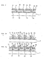
- Fig. 1 schematically illustrate the steps of manufacturing a film type solar battery in sequence, in one embodiment of the present invention.
- parts corresponding functionally to those already described with reference to Fig. 2 are therefore designated by the same reference numerals or characters.
- Fig. 1a illustrates a pattern of a conductive layer according to one embodiment of the invention.
- conductive films 51, 52, 53, 54 and so forth are formed by printing the conductive films of a glass substrate l with conductive paste containing silver by a screen printing technique, followed by sintering at about 500°C for about ten minutes.
- a transparent electrode layer is formed to a thickness of 0.4 to 1 ⁇ m by an electronic beam vacuum deposition method or hot CVD method in such a manner as to cover all the conductive films.
- the transparent electrode layer thus formed is scanned with a yttrium-aluminum-garnet (YAG) laser beam about 50 ⁇ m in diameter in such a manner that the laser beam is applied along a line about 20 ⁇ m left of each of the conductive films, 51, 52, 53, 54 and so forth, thereby to pattern (form) transparent electrodes 21, 22, 23, 24 and so forth as shown in Fig. 1b.
- a suitable output power of the laser in this operation is 2 x 10⁵ to 5 x 10⁵ W/cm2.
- an a-Si layer consisting of a p-layer about 100 ⁇ in thickness, an i-layer about 0.5 ⁇ m in thickness and a n-layer of about 500 ⁇ in thickness were laid one on another in the stated order as viewed from the side of the transparent electrodes. These layers are formed in the stated manner so as to cover all the transparent electrodes.
- the p-layer can be formed by decomposing a reaction gas which is formed by mixing B2H6 of about 1% with SiH4 and subjecting the gas to glow discharge.
- the i-layer can be formed by decomposing SiH4 by the same technique.
- the n-layer can be formed by decomposing a gas which is prepared by mixing PH3 of about 1% with SiH4.
- a laser beam of about 50 ⁇ m in diameter is applied to the a-Si layer 3 formed over the conductive films 51, 52, 53, 54 and so on as described above.
- the power of the applied laser beam is 2 x 10⁵ W/cm2 or less, preferably 0.5 x 10⁵ to 2 x 10⁵ W/cm2.
- the a-Si layer becomes molten and evaporates at irradiated regions 61, 62, 63, 64 and so forth and the heat produced in this operation makes the irradiated regions polycrystalline in the direction of the thickness of the a-Si layer 3 as shown in Fig. 1c.
- a metal electrode layer for example, aluminum
- a metal electrode layer for example, aluminum
- Irradiated regions 61, 62, 63, 64 of the a-Si layer which have been made polycrystalline are low in resistance, having a conductivity 1,000 times as high as that of the surrounding a-Si layer.
- the metal electrode layer of aluminum or the like is electrically connected to the transparent electrodes through the polycrystalline regions 61, 62, 63, 64 as shown in Fig. 1d.
- the metal electrode layer is scanned with a laser beam about 50 ⁇ m in diameter in such a manner that the laser beam is applied along a line on the righthand side of each of the polycrystalline regions, thereby to pattern or form individual metal electrodes 41, 42, 43, 44.
- a suitable power of the laser beam was found to be 5 x 10⁶ to 10 x 106 W/cm2, and the separation belts, or material removed from between the electrodes 81, 82, 83, 84 were found to be about 40 ⁇ m in width.
- Conductive films 51, 52, 53, 54 formed on the glass substrate l absorb the energy of the laser beam which otherwise may be lost, thus contributing to the formation of the polycrystalline regions in the a-Si layer. Even if the energy of the laser beam utilized is so large that, as shown in Fig. 2a, the a-Si layer 3 and the transparent electrodes 21, 22, 23, 24 are cut to form gaps 71, 72, 73, 74, Fig. 3a, these gaps are filled with metal in the subsequent step of forming the metal electrode layer. As shown in Fig. 3b, the metal electrodes 41, 42, 44 are connected to the transparent electrodes 21, 22, 23, through a metal, such as aluminum, which fills in the gaps 72, 73, 74.
- the elements can be connected in series to one another no matter how non-uniform the surface and thickness of the a-Si layer 3 when employing the method of the present invention.
- the conductive films 51, 52, 53, 54 are formed by printing them on the substrate with a conductive paste; however, they may also be formed by vacuum-depositing metal through a mask. They may also be formed by depositing a metal film layer which is thereafter subjected to patterning.
- these conductive films should be resistant to temperatures as high as about 500°C so as to withstand the temperature which is used in forming the a-Si layer.
- the conductive film should be scarcely scattered when irradiated by the laser beam.
- a conductive layer 51, 52, 53, 54 is provided between the translucent insulated substrate l and the transparent electrode layer 21, 22, 23, 24 with each conductive layer positioned below its respective polycrystalline region 61, 62, 63, 64 of a-Si layer 3.
- the conductive energy 51, 52, 53, 54 also prevents the transmission of the laser beam through the transparent substrate l.
- the present battery will still contain an electrical connection between the metal electrodes 41, 42, 43, and 44 and their respective transparent electrodes 21, 22, 23 and 24.
- the non-crystalline semiconductor layer is not uniform in thickness or its surface fluctuates in reflection factor
- sites for polycrystalline regions can be formed in the non-crystalline semiconductor layer by using the same laser beam. Even if the site comprises a void, the subsequent metal layer forming step will provide the electrical connection with the transparent electrode.
- automation of the manufacture of the solar battery of the invention can be readily achieved.
Landscapes
- Photovoltaic Devices (AREA)
Applications Claiming Priority (2)
| Application Number | Priority Date | Filing Date | Title |
|---|---|---|---|
| JP60205591A JPS6265480A (ja) | 1985-09-18 | 1985-09-18 | 薄膜太陽電池装置 |
| JP205591/85 | 1985-09-18 |
Publications (3)
| Publication Number | Publication Date |
|---|---|
| EP0215482A2 true EP0215482A2 (de) | 1987-03-25 |
| EP0215482A3 EP0215482A3 (en) | 1989-05-31 |
| EP0215482B1 EP0215482B1 (de) | 1992-03-04 |
Family
ID=16509415
Family Applications (1)
| Application Number | Title | Priority Date | Filing Date |
|---|---|---|---|
| EP86112879A Expired - Lifetime EP0215482B1 (de) | 1985-09-18 | 1986-09-18 | Sonnenbatterie und Herstellungsverfahren |
Country Status (4)
| Country | Link |
|---|---|
| US (1) | US4734379A (de) |
| EP (1) | EP0215482B1 (de) |
| JP (1) | JPS6265480A (de) |
| DE (1) | DE3684066D1 (de) |
Families Citing this family (3)
| Publication number | Priority date | Publication date | Assignee | Title |
|---|---|---|---|---|
| US4968354A (en) * | 1987-11-09 | 1990-11-06 | Fuji Electric Co., Ltd. | Thin film solar cell array |
| US4978601A (en) * | 1989-10-30 | 1990-12-18 | International Lead Zinc Research Organization, Inc. | Lead alloy battery grids by laser treatment |
| EP2261976A1 (de) * | 2009-06-12 | 2010-12-15 | Applied Materials, Inc. | Halbleiterbauteilmodul, Verfahren zur Herstellung eines Halbleiterbauteilmoduls, Vorrichtung zur Herstellung von Halbleiterbauteilmodulen |
Family Cites Families (17)
| Publication number | Priority date | Publication date | Assignee | Title |
|---|---|---|---|---|
| GB2108755B (en) * | 1981-09-26 | 1985-07-10 | Matsushita Electric Industrial Co Ltd | Thin film devices having diffused interconnections |
| US4428110A (en) * | 1981-09-29 | 1984-01-31 | Rca Corporation | Method of making an array of series connected solar cells on a single substrate |
| US4407695A (en) * | 1981-12-31 | 1983-10-04 | Exxon Research And Engineering Co. | Natural lithographic fabrication of microstructures over large areas |
| US4396793A (en) * | 1982-04-12 | 1983-08-02 | Chevron Research Company | Compensated amorphous silicon solar cell |
| US4570332A (en) * | 1982-05-10 | 1986-02-18 | Sharp Kabushiki Kaisha | Method of forming contact to thin film semiconductor device |
| JPS59115574A (ja) * | 1982-12-23 | 1984-07-04 | Semiconductor Energy Lab Co Ltd | 光電変換装置作製方法 |
| US4591892A (en) * | 1982-08-24 | 1986-05-27 | Semiconductor Energy Laboratory Co., Ltd. | Semiconductor photoelectric conversion device |
| JPS5952883A (ja) * | 1982-09-20 | 1984-03-27 | Fuji Electric Corp Res & Dev Ltd | 太陽電池 |
| JPS5954274A (ja) * | 1982-09-22 | 1984-03-29 | Sanyo Electric Co Ltd | 光起電力装置 |
| US4532537A (en) * | 1982-09-27 | 1985-07-30 | Rca Corporation | Photodetector with enhanced light absorption |
| JPS5986269A (ja) * | 1982-11-09 | 1984-05-18 | Semiconductor Energy Lab Co Ltd | 光電変換装置の作製方法 |
| US4528065A (en) * | 1982-11-24 | 1985-07-09 | Semiconductor Energy Laboratory Co., Ltd. | Photoelectric conversion device and its manufacturing method |
| JPS5994884A (ja) * | 1982-11-24 | 1984-05-31 | Semiconductor Energy Lab Co Ltd | 光電変換装置の作製方法 |
| JPS59107579A (ja) * | 1982-12-11 | 1984-06-21 | Semiconductor Energy Lab Co Ltd | 光電変換装置の作製方法 |
| US4461922A (en) * | 1983-02-14 | 1984-07-24 | Atlantic Richfield Company | Solar cell module |
| US4517403A (en) * | 1983-05-16 | 1985-05-14 | Atlantic Richfield Company | Series connected solar cells and method of formation |
| JPS59220978A (ja) * | 1983-05-31 | 1984-12-12 | Sanyo Electric Co Ltd | 光起電力装置の製造方法 |
-
1985
- 1985-09-18 JP JP60205591A patent/JPS6265480A/ja active Granted
-
1986
- 1986-09-16 US US06/908,032 patent/US4734379A/en not_active Expired - Lifetime
- 1986-09-18 EP EP86112879A patent/EP0215482B1/de not_active Expired - Lifetime
- 1986-09-18 DE DE8686112879T patent/DE3684066D1/de not_active Expired - Lifetime
Also Published As
| Publication number | Publication date |
|---|---|
| EP0215482B1 (de) | 1992-03-04 |
| JPS6265480A (ja) | 1987-03-24 |
| JPH055194B2 (de) | 1993-01-21 |
| US4734379A (en) | 1988-03-29 |
| EP0215482A3 (en) | 1989-05-31 |
| DE3684066D1 (de) | 1992-04-09 |
Similar Documents
| Publication | Publication Date | Title |
|---|---|---|
| EP0195148B1 (de) | Photovoltaische Vorrichtung und deren Herstellungsverfahren | |
| US5133809A (en) | Photovoltaic device and process for manufacturing the same | |
| US4532371A (en) | Series-connected photovoltaic array and method of making same | |
| JP4796947B2 (ja) | 集積型薄膜太陽電池及びその製造方法 | |
| US4633034A (en) | Photovoltaic device and method | |
| US4590327A (en) | Photovoltaic device and method | |
| US6080928A (en) | Photovoltaic element array and method of fabricating the same | |
| US4496788A (en) | Photovoltaic device | |
| US4824488A (en) | Photovoltaic device | |
| US4879251A (en) | Method of making series-connected, thin-film solar module formed of crystalline silicon | |
| US5147468A (en) | Photovoltaic semiconductor device and method for manufacturing the same | |
| US4668840A (en) | Photovoltaic device | |
| EP0221523A2 (de) | Halbleitervorrichtung | |
| KR101942783B1 (ko) | 태양 전지 및 이의 제조 방법 | |
| US5385614A (en) | Series interconnected photovoltaic cells and method for making same | |
| GB2077038A (en) | Fabrication of a solar battery using laserscribing | |
| EP2023395A2 (de) | Fotovoltaische Vorrichtung und Herstellungsverfahren dafür | |
| CN1007103B (zh) | 光电型器件及其制造方法 | |
| EP0217405A1 (de) | Durchsichtige leitende Schicht und Verfahren zu deren Herstellung | |
| US4954181A (en) | Solar cell module and method of manufacture | |
| JPH1079522A (ja) | 薄膜光電変換装置およびその製造方法 | |
| EP0153043A2 (de) | Ohmische Kontaktschicht | |
| EP0215482A2 (de) | Sonnenbatterie und Herstellungsverfahren | |
| KR20190008390A (ko) | 태양 전지 및 이의 제조 방법 | |
| US4764476A (en) | Method of making photoelectric conversion device |
Legal Events
| Date | Code | Title | Description |
|---|---|---|---|
| PUAI | Public reference made under article 153(3) epc to a published international application that has entered the european phase |
Free format text: ORIGINAL CODE: 0009012 |
|
| AK | Designated contracting states |
Kind code of ref document: A2 Designated state(s): DE FR GB |
|
| PUAL | Search report despatched |
Free format text: ORIGINAL CODE: 0009013 |
|
| AK | Designated contracting states |
Kind code of ref document: A3 Designated state(s): DE FR GB |
|
| 17P | Request for examination filed |
Effective date: 19891017 |
|
| 17Q | First examination report despatched |
Effective date: 19891206 |
|
| GRAA | (expected) grant |
Free format text: ORIGINAL CODE: 0009210 |
|
| AK | Designated contracting states |
Kind code of ref document: B1 Designated state(s): DE FR GB |
|
| REF | Corresponds to: |
Ref document number: 3684066 Country of ref document: DE Date of ref document: 19920409 |
|
| ET | Fr: translation filed | ||
| PLBE | No opposition filed within time limit |
Free format text: ORIGINAL CODE: 0009261 |
|
| STAA | Information on the status of an ep patent application or granted ep patent |
Free format text: STATUS: NO OPPOSITION FILED WITHIN TIME LIMIT |
|
| 26N | No opposition filed | ||
| REG | Reference to a national code |
Ref country code: GB Ref legal event code: 732E |
|
| REG | Reference to a national code |
Ref country code: FR Ref legal event code: TP |
|
| REG | Reference to a national code |
Ref country code: GB Ref legal event code: IF02 |
|
| PGFP | Annual fee paid to national office [announced via postgrant information from national office to epo] |
Ref country code: FR Payment date: 20030909 Year of fee payment: 18 |
|
| PGFP | Annual fee paid to national office [announced via postgrant information from national office to epo] |
Ref country code: GB Payment date: 20030917 Year of fee payment: 18 |
|
| PGFP | Annual fee paid to national office [announced via postgrant information from national office to epo] |
Ref country code: DE Payment date: 20030925 Year of fee payment: 18 |
|
| PG25 | Lapsed in a contracting state [announced via postgrant information from national office to epo] |
Ref country code: GB Free format text: LAPSE BECAUSE OF NON-PAYMENT OF DUE FEES Effective date: 20040918 |
|
| PG25 | Lapsed in a contracting state [announced via postgrant information from national office to epo] |
Ref country code: DE Free format text: LAPSE BECAUSE OF NON-PAYMENT OF DUE FEES Effective date: 20050401 |
|
| GBPC | Gb: european patent ceased through non-payment of renewal fee |
Effective date: 20040918 |
|
| PG25 | Lapsed in a contracting state [announced via postgrant information from national office to epo] |
Ref country code: FR Free format text: LAPSE BECAUSE OF NON-PAYMENT OF DUE FEES Effective date: 20050531 |
|
| REG | Reference to a national code |
Ref country code: FR Ref legal event code: ST |