EP0215311A2 - Laser diode driving circuit - Google Patents
Laser diode driving circuit Download PDFInfo
- Publication number
- EP0215311A2 EP0215311A2 EP86111421A EP86111421A EP0215311A2 EP 0215311 A2 EP0215311 A2 EP 0215311A2 EP 86111421 A EP86111421 A EP 86111421A EP 86111421 A EP86111421 A EP 86111421A EP 0215311 A2 EP0215311 A2 EP 0215311A2
- Authority
- EP
- European Patent Office
- Prior art keywords
- semiconductor device
- current
- circuit
- voltage
- device driving
- Prior art date
- Legal status (The legal status is an assumption and is not a legal conclusion. Google has not performed a legal analysis and makes no representation as to the accuracy of the status listed.)
- Withdrawn
Links
Images


Classifications
-
- H—ELECTRICITY
- H01—ELECTRIC ELEMENTS
- H01S—DEVICES USING THE PROCESS OF LIGHT AMPLIFICATION BY STIMULATED EMISSION OF RADIATION [LASER] TO AMPLIFY OR GENERATE LIGHT; DEVICES USING STIMULATED EMISSION OF ELECTROMAGNETIC RADIATION IN WAVE RANGES OTHER THAN OPTICAL
- H01S3/00—Lasers, i.e. devices using stimulated emission of electromagnetic radiation in the infrared, visible or ultraviolet wave range
-
- G—PHYSICS
- G11—INFORMATION STORAGE
- G11B—INFORMATION STORAGE BASED ON RELATIVE MOVEMENT BETWEEN RECORD CARRIER AND TRANSDUCER
- G11B7/00—Recording or reproducing by optical means, e.g. recording using a thermal beam of optical radiation by modifying optical properties or the physical structure, reproducing using an optical beam at lower power by sensing optical properties; Record carriers therefor
- G11B7/12—Heads, e.g. forming of the optical beam spot or modulation of the optical beam
- G11B7/125—Optical beam sources therefor, e.g. laser control circuitry specially adapted for optical storage devices; Modulators, e.g. means for controlling the size or intensity of optical spots or optical traces
- G11B7/126—Circuits, methods or arrangements for laser control or stabilisation
-
- H—ELECTRICITY
- H01—ELECTRIC ELEMENTS
- H01S—DEVICES USING THE PROCESS OF LIGHT AMPLIFICATION BY STIMULATED EMISSION OF RADIATION [LASER] TO AMPLIFY OR GENERATE LIGHT; DEVICES USING STIMULATED EMISSION OF ELECTROMAGNETIC RADIATION IN WAVE RANGES OTHER THAN OPTICAL
- H01S5/00—Semiconductor lasers
- H01S5/06—Arrangements for controlling the laser output parameters, e.g. by operating on the active medium
- H01S5/068—Stabilisation of laser output parameters
- H01S5/0683—Stabilisation of laser output parameters by monitoring the optical output parameters
Definitions
- the present invention relates to a laser diode driving circuit, more particularly to a laser diode driving circuit which controls a laser diode so as to generate a predetermined light output stably and fast.
- optical information processors including optical disc device, optical communications devices, and others
- a laser diode as a light source in such a device, it is important to generate a light output from the laser diode fast and stably.
- a laser diode has a relatively large forward voltage drop for a forward current so that it is accompanied by a considerable temperature rise, and like many of the semiconductor elements, it has a temperature dependence.
- temperature rise is handled by the provision of a cooling means.
- temperature rise cannot be handled appropriately by means of a cooling means alone, leading to a fear of having a breakdown of the laser diode.
- the laser diode be able to generate stably a prescribed light output even under changes in the temperature, there are few laser diodes that give sufficient consideration to the temperature compensation so as to control stably the light output of the laser diode for variations in the temperature, so that it becomes also necessary to have a sufficient measure for the temperature compensation.
- An object of the present invention is to provide a laser diode driving circuit which controls stably and fast the light output of a laser diode to a prescribed level by means of a relatively simple circuit configuration.
- Another object of the present invention is to provide a laser diode driving circuit which can prevent the breakdown of the laser diode due to flow of an excess current in it, and control its stable operation.
- Still another object of the present invention is to provide a laser diode driving circuit which is capable of variably modulating the level of light output precisely to each of a plurality of levels.
- Still further object of the present invention is to provide a laser diode driving circuit which is capable of stably controlling the light output level of the laser diode to a prescribed value for variations in temperature.
- Still further object of the present invention is to provide a laser diode driving circuit which is capable of controlling the laser diode to prevent its breakdown as a result of an abnormal operation caused by malfunctions due to drop in the supply voltage.
- light output of the laser diode is detected to be converted to an electrical signal that corresponds to the level of light output, the electrical signal is compared with a reference signal, and a control is given so as to let the electrical signal to have a prescribed value that corresponds to the reference signal. Therefore, it is possible to control the light output of the laser diode stably at a prescribed value. Further, its circuit configuration is simple so that the response characteristics are extremely satisfactory, the high speed controllability is excellent, making it possible to realize a high degree of economy.
- the forward current in the laser diode is detected and the forward current is controlled when it exceeds a prescribed current value. Therefore, it is possible to prevent the breakdown of the laser diode due to excess current, and to realize a stable operation of the system.
- a plurality of reference signals are generated, and the electrical signal that corresponds to the level of light output of the laser diode is controlled so as to be equal to the value that corresponds to a reference signal selected from among a plurality of reference signals. Therefore, it is possible to variably modulate the light output of the laser diode in a free fashion.
- a reference signal source which generates a reference signal with signal level that has the opposite temperature characteristics to the temperature coefficient of the light output level characteristics for the laser diode, the light output from the laser diode is converted to an electrical signal, and the electrical signal is compared with the reference signal to be controlled so as to have a value that corresponds to the reference signal. Therefore, it is possible to control the light output of the laser diode to a predetermined value, even when there are generated temperature changes in the laser diode.
- the power supply voltage is detected, and the operation of the laser diode is interrupted when the power supply voltage is at a predetermined value. Therefore, needless to mention the case of a drop in the power supply voltage for some reason, but also in the low voltage state which the power supply voltage has to go through in the closing or opening of the power supply, it is possible to prevent the breakdown of the laser diode that may be caused by the generation of an abnormally high light output due to abnormal operation of the laser diode.
- the laser diode driving circuit has, for example, a laser diode LD which is used as the light source for the optical disc device and a photodiode PD which converts the light output from the laser diode LD to an electrical signal.
- the laser diode LD and the photodiode PD are built in a package II.
- a common connecting terminal Ila which jointly connects the anode of the laser diode LD and the cathode of the photodiode PD, a cathode terminal lib of the laser diode LD, and an anode terminal Ilc of the photodiode PD.
- One of the output surfaces of the laser diode LD is placed facing the photodiode PD, and a light output P o is taken out from the other output surface to the outside.
- the cathode terminal IIb of the laser diode LD is connected to the reference voltage (ground).
- a reference current source I To the anode terminal IIc are connected a reference current source I and a current controlling means 5 which controls the forward current that is supplied to the laser diode LD so as to bring the photoval- taic current I s in the photodiode PD that monitors the light output P o of the laser diode LD to be equal to the reference current I ref that flows in the reference current source I.
- the current controlling means 5 comprises an inverting amplifier 2 which is connected to the anode terminal IIc of the photodiode PD and a feedback circuit 3 which feeds back the inverted and amplified output from the inverting amplifier 2 to the forward current circuit 4 that is connected to the common connecting terminal Ila, in order to invert and amplify the difference current between the photovoltaic current I s and the reference current I ref that flows in the reference current source I.
- Such a laser driving circuit can easily be integrated. Needless to say, however, under the current circumstances, it is preferred to have the laser diode and the photodiode as externally attachable parts. Accordingly, it is conceivable to integrate the part of Fig. I (a) which excludes LD and PD that are enclosed in a broken line II. Further, from the viewpoint of ease in adjusting, the reference current source I ref may be set as an external resistor for the IC.
- a modification circuit of the first embodiment of a laser driving circuit according to the present invention.
- a common connecting terminal Ila is connected, from a positive power supply line 2a, to a forward current circuit 4 which has a driving transistor Q2 and a resistor R, that regulates the forward current If to a maximum rated value.
- Reference numeral 5 is a bias current circuit for the driving transistor Q 2 , and serves also as the output circuit for the controlling transistor Q,.
- the controlling transistor Q constitutes an inverting amplification means 2, and its base is connected to the anode terminal IIc of the photodiode PD, its emitter is connected to a power supply line 2b, and its collector is connected to the base of the driving transistor Q z .
- the anode terminal IIc of the photodiode PD is connected via a reference current source I that supplies a reference current to the power supply line 2b.
- the cathode of the laser diode LD is connected via the cathode terminal lib to the power supply line 26.
- Figure 2 is a characteristic diagram for illustrating the relation between the forward current If of the laser diode LD and the light output P o
- Fig. 3 is a characteristic diagram for illustrating the relation between the light output P o of the laser diode LD and the monitoring current (photovoltaic current) Is that is generated in the photodiode PD.
- a light output P o by the oscillation of the laser diode LD when the forward current If reaches a certain "threshold current", for instance 60 mA, and thereafter the light output P o increases in proportion to the forward current If.
- the photodiode PD generates a photovoltaic current Is upon receipt of the light output P o .
- the photovoltaic current Is increases in proportion to the light output P o .
- a numerical example that shows the relation among the forward current If , the light output P o , and the photovoltaic current Is at the room temperature is:
- the photovoltaic current Is of the photodiode PD is proportional to the light output P o as in the above, it becomes possible to control the light output P o at a constant value by detecting the photovoltaic current Is and feedback-controlling the light output P o .
- the light output P o is arranged to have a constant value by controlling it so as to bring the detected photovoltaic current Is to be equal to the value that corresponds to the reference current I ref -Namely, in the state in which the relation between the photovoltaic current Is and the reference current I ref is Is ⁇ I ref , there flows no current to the base of the controlling transistor Q, so that the controlling transistor Q, is in off-state.
- the driving transistor Q 2 is brought to on-state by the flow of a bias current I b from the bias current circuit 5, and these flows in the laser diode LD a maximum upper limit current that is prescribed by the current controlling resistor R, to increase the light output P o .
- the driving transistor Q is driven by the inverting amplification current of the controlling transistor Q, and the driving transistor Q 2 controls the forward current If of the laser diode LD in response to the size of the difference current between the photovoltaic current Is and the reference current I ref , reducing the value of the current I f .
- the forward current If of the laser diode LD is controlled to become 90 mA that corresponds to this reference current 0.75 mA.
- control is carried out to have a constant light output P o of 10 mW.
- the control current that is obtained by the forward current circuit 4 includes the component of the photovoltaic current I s that flows to the photodiode PD. Therefore, the control operation for the forward current If generates an error which is equal to the amount of photovoltaic current I s .
- the photovoltaic current Is has a value which is less than 1/100 of the forward current I f , as shown in the above example. Therefore, the above error is almost negligible so that the control current that flows in the forward current circuit 4 may safely be regarded to be equal to the forward current If of the laser diode LD.
- Fig. 4 a concrete example of the first embodiment.
- the laser diode LD is driven by high frequency pulsed current, and its pulsed light output is attempted to be detected by a photodiode sensor PD 2 that is provided externally.
- reference numeral 6 is a switching circuit for switch-driving the laser diode LD.
- This fast switching circuit consists of a switching transistor Q 3 , resistors R 5 to R., a capacitor C 2 , and a diode D.
- Reference numeral 7 is a voltage input terminal for inputting a pulsed voltage for driving the switching circuit 6.
- the sense amplifier for outputting a voltage output V o from an output terminal 8 by amplifying the detected photovoltaic current I o .
- the sense amplifier consists of an operating amplifier A4 and a feedback resistor R 4 .
- the light output P o of the laser diode LD is controlled so as to let the photovoltaic current Is of the photodiode PD have a value that corresponds to 73 ⁇ A of the reference current I ref . Then, by applying the proportionality relation between the two quantities given by Eq. (I) as it is, there will be obtained a light output P o of about I mW from the laser diode LD.
- FIG. 5 (A), 5 (B), and 5 (C) The pulse response characteristics of such a concrete example, obtained when the laser diode LD is pulse-driven by inputting from the voltage input terminal 7 a pulsed voltage of repetition frequency of I MHz as the input voltage V;, are shown in Figs. 5 (A), 5 (B), and 5 (C).
- Figure 5 (A) is a diagram for illustrating the response characteristics between the input voltage V i and the anode voltage (driving voltage) V d of the laser diode LD
- Fig. 5 (B) is a diagram for illustrating the response characteristics between the input voltage V I and the forward current If of the laser diode LD
- Fig. 5 - (C) is a diagram for illustrating the response characteristics between the input voltage V 1 and the voltage output V o to the outside.
- the pulsed output voltage V o which is output from the output terminal 8 through the external detection system that consists of the photodiode sensor PD 2 and the sense amplifier, has an amplitude of about 0.2 V and the rise time t r and the fall time t f of about 40 nsec and 50 nsec, respectively, which shows a very fast pulse response. It was confirmed that the light output P o in such a pulse drive can also be controlled to a constant value in a stable manner.
- the rise time t r and the fall time t f are values that include the response lag of the sense amplifier itself and others.
- Fig. 6 there is shown a first modification to the first embodiment.
- the controlling transistor use is made of a junction type field effect transistor (JFET) Q 4 , instead of the npn transistor Q, in the first embodiment, to enhance further the control accuracy of the light output Po.
- JFET junction type field effect transistor
- the reference current ref is given a value which is less than about 100 ⁇ A, and the light ouput P o is controlled in such a way as the photovoltaic current I s of the photodiode PD thus generated to have a value corresponding to the reference current I ref .
- the photovoltaic current Is of the photodiode PD has a small value as mentioned in the above so that when an npn transistor Q, is used as the controlling transistor as in the first embodiment, there will flow a base current of the order of ⁇ A in the npn transistor Q,, and hence a control error of the size of the base current will be generated due to inclusion of the base current in the photovoltaic current I s .
- the above control error is arranged to be eliminated by making the gate current to be almost nonexistent.
- FIG. 7 there is shown a second modification to the first embodiment.
- control accuracy is attempted to be improved further by connecting a voltage comparator VC between the junction of the photodiode PD and the reference current source I, and the base of the controlling transistor Q,.
- the reference voltage V ref of the voltage comparator VC is set at the ground potencial.
- the signal that corresponds to the difference between the reference current I ref of the reference current source I and the photovoltaic current I s of the photodiode PD is inverted and amplified by the controlling transistor Q, via the voltage comparator VC.
- the amplified output is fed back to the forward current circuit 4 to control the forward current If of the laser diode LD to a current value that corresponds to the reference current I ref .
- Such a fundamental operation is similar to the case of the first embodiment.
- the anode voltage of the photodiode PD is set to be equal to the reference voltage Vref of the voltage comparator VC, namely, the ground potencial.
- the anode potential of the photodiode PD When the anode of the photodiode PD is connected directly to the base of the controlling transistor Q, the anode potential of the photodiode PD has a temperature dependence under the influence of the temperature characteristics of the controlling transistor Q, which generates a temperature dependence also in the stabilized operation of the light output.
- the voltage of the photodiode PD is prescribed to the reference voltage V ref of the voltage comparator VC, and the effect of the temperature characteristics of the controlling transistor Q, is eliminated.
- V ref may be set at a potential other than that of the ground. By so doing, it will become possible to set the reverse bias voltage for the photodiode at a larger value.
- the possible connection modes of the laser diode LD and the photodiode PD include (a) a mode of jointly connecting the anode of the laser diode LD and the cathode of the photodiode PD; - (b) a mode of jointly connecting the cathode of the laser diode LD and the anode of the photodiode PD; (c) a mode of mutually and jointly connecting the cathodes of the laser diode LD and the photodiode PD; (d) a mode of mutually and jointly connecting the anodes of the laser diode LD and the photodiode PD; and (e) a mode that does not jointly connect the laser diode LD and the photodiode PD.
- the modifications to the laser diode driving circuit that are constructed in accordance with each of the connection modes that are enumerated in the above.
- Fig. 8 (A) shows a third modification to the present invention.
- This modification uses a npn transistor as a driving transistor Q 2 , and by connecting the junction of the reference current source I and the photodiode PD directly to the base of the driving transistor Q 2 to omit the arrangement of the transistor that corresponds to the controlling transistor Q, in the first embodiment, with a main purpose of further simplifying the circuit configuration.
- the laser diode LD is connected to the emitter circuit of the driving transistor Q, which is connected as an emitter follower.
- the light output P o of the laser diode LD is controlled to become constant at an output value for which the photovoltaic current Is of the photodiode PD equals the reference current I ref .
- the number of components in the circuit is small so that a more satisfactory effect can be obtained in view of the fast driving capability.
- Figure 8 (B) is a complementary circuit to the circuit shown in Fig. 8 (A) obtained by the use of an npn transistor as the driving transistor Q 2 '. Its operation is similar to that of the circuit shown in Fig. 8 (A).
- a fourth modification to the present invention is shown a fourth modification to the present invention.
- a npn transistor is used as the driving transistor Q 2
- the aspect that the junction of the reference current source I and the photodiode PD is connected to the base of the driving transistor Q 2 is the same as in the third modification shown in Fig. 8 (A).
- the laser diode LD is connected to the collector circuit of the driving transistor Q 2 .
- the operation of detecting a photovoltaic current Is that corresponds to the light output P o by the photodiode PD, and controlling, by the feedback of the detected value, the light output P o so as to be constant at an output value for which the photovoltaic current Is becomes equal to the value that corresponds to the reference current I ref , is similar to the case of the third modification.
- Figure 9 (B) is a complementary circuit to the circuit of Fig. 9 (A), obtained by the use of an npn transistor as the driving transistor Q 2 '. Its operation is similar to the case of Fig. 9 (A).
- Fig. 10 (A) is shown a fifth modification to the present invention.
- the cathode of the laser diode LD and the cathode of the photodiode PD are jointly connected, and it shows the circuit configuration for the case in which there exists a restriction that a common connecting terminal is drawn out from the connecting point.
- the sum of the controlling current that flows in the driving transistor Q2 and the photovoltaic current I s that flows in the photodiode PD flows in the laser diode LD as a forward current If. Because of this, between the forward current If and the controlling current, there exists an error which corresponds to the photovoltaic current I s . However, the photovoltaic current Is has a value which is less than 1/100 of the forward current If as mentioned earlier so that the above error can be neglected almost completely, and that controlling current that flows in the driving transistor Q 2 may safely be regarded to be equal to the forward current If of the laser diode.
- the stabilized controlling action of the light output P o by means of the present modification is substantially the same as in the third modification.
- Figure 10 (B) is constructed as a complementary circuit to the circuit shown in Fig. 10 (A) by employing a npn transistor as the driving transistor Q 2 '. Its operation is approximately the same as that of Fig. 10 (A).
- Figure II shows a second embodiment of the present invention.
- the second embodiment is obtained by attaching an excess current protective circuit 10 to the laser diode driving circuit which has a controlling circuit for output stabilization shown in the first embodiment.
- the current driving resistor R which was connected in series to the anode of the laser diode in the first embodiment is taken away, and in its place there is connected in series a voltage detecting resistor R 10 to the cathode of the laser diode LD to let the resistor R 10 to play the function of a current limiting resistor to some extent.
- a forward current limiting circuit (forward limiting means) 12 that has a limiting transistor Q 5 is connected to a forward current circuit 4.
- the mode of connection is such that the collector of the limiting transistor Q s is connected to the common connecting terminal Ila, and its emitter is connected to a negative power supply line 2b.
- the detecting resistor R 10 Between the cathode terminal Ilb of the laser diode in the forward current circuit 4 and the power supply line 2b, there is connected the detecting resistor R 10 for taking out the voltage drop due to the forward current I, as a detected voltage, and the take-out point 3a of the detected voltage is connected to the base of the limiting transistor Q s .
- the resistance of the detecting resistor R 1 P 0 is prescribed as where I fmax is the maximum rated value (limited current value) of the forward current I, of the laser diode LD and V BE is the base-emitter voltage that is needed for making the limiting transistor Q 5 a conducting state (assuming that the symbol for the resistor R, o represents the resistance as is).
- Figure 12 (A) is a characteristic diagram for showing the relation between the forward current I, of the laser diode LD and the light output P o
- Fig. 12 (B) is a characteristics diagram for showing the relation between the light output P o of the laser diode LD and the monitoring current (photovoltaic current I s ) that is generated in the photodiode PD.
- the laser diode LD outputs a light output P o by laser oscillation when the forward current If reaches a certain "threshold current value" If', and thereafter the light output P o increases in proportion to the forward current I,.
- the photovoltaic current Is is generated upon receipt of the light output P o in which the photovoltaic current Is increases in proportion to the light output P o .
- the photovoltaic current Is that is detected by the photodiode PD is proportional to the light output P o , so that the light output P o is feedback-controlled at a constant value in a stabilized manner, so as to have a value that corresponds to the reference current I ref .
- the maximum consumed power P dmax of the laser diode LD is given by
- the laser diode LD maintains a normal laser oscillation state in the range below the maximum consumed power P dmax .
- the detected voltage I f .R 10 which is detected by the detecting resistor R 10 has a value less than the voltage V BE between the base and the emitter of the limiting transistor Q 5 , so that the forward current limiting circuit 12 is not affected at all.
- the forward current limiting circuit 12 When the excess current state is stopped, the forward current limiting circuit 12 returns to the original nonactive state, and the system goes back to the normal output stabilized state by the driving system circuit.
- a second modification to the second embodiment is shown a second modification to the second embodiment.
- a detecting resistor R, o ' is connected between the emitter of the driving transistor Q 2 and the jointly connecting terminal la
- the limiting transistor Q 5 ' is connected between the base of the driving transistor Q 2 and the jointly connecting terminal la.
- the detected voltage take-out point 3b is connected to the base of the limiting transistor G 5 '.
- a forward current limiting circuit 12' is arranged in a part of the forward current circuit 4 on the side of anode of the lase diode LD.
- Other configuration is approximately the same as that shown in Fig. II.
- current that flows in the detecting resistor R, a ' includes the photovoltaic current I s that flows in the laser diode LD in addition to the forward current I, and the photovoltaic current I s becomes a factor in the errors.
- the photovoltaic current I s has a value less than 1/100 of the forward current I f as mentioned earlier, so that the error in the detected voltage due to the photovoltaic current I s can be neglected almost completely.
- Figure 15 shows a third modification to the present invention. This modification is obtained from the second modification shown in Fig. II by replacing the reference current source I by a reference current switching circuit J,.
- Fig. 15 components identical to those in Fig. 11 are given identical symbols to omit repeated explanation.
- Reference numeral 14a is a first reference current source which sets the reference current to I refl
- 14b is a second reference current source which sets the reference current to I ref2
- Reference numerals 15a and 15b are the first and the second differential amplifiers, and the two differential amplifiers 15a and 15b constitute the selector switch for switching between the reference current sources 14a and 14b.
- the first differential amplifier 15a consists of a pair of transistors Q 6 and Q, while the second differential amplifier 15b consists of another pair of transistors Q 8 and Qg.
- the collectors of the transistors Q 6 of the first differential amplifier 15a and the transistor Q 8 of the second differential amplifier 15b are jointly connected, and the junction is connected to the anode terminal IIc of the photodiode PD.
- the common junction of the emitters of the first differential amplifier 15a is connected to the first reference current source 14a
- the common junction of the emitters of the second differential amplifier 15b is connected to the second reference current source 14b.
- the selector switch that consists of the differential amplifiers 15a and 15b has a high speed switching capability that corresponds to the cut-off frequency of each of the transistors Q 6 to Q 7 .
- Figure 16 (A) is a characteristic diagram for showing the relation between the forward current If of the laser diode LD and the light output P o
- Fig. 16 (B) is a characteristic diagram for showing the relation between the light output P o of the laser diode LD and the monitoring current (photovoltaic current) I s that is generated in the photodiode PD.
- Fig. 16 (A) it will be seen that the laser diode LD is oscillated to give a light output when its forward current I f reaches a certain "threshold current value", and thereafter the light output increases in proportion to the forward current If .
- the characteristic line for the forward current If versus the light output P o in this proportional region is fairly steep similar to the forward characteristic of the ordinary semiconductor.
- the photodiode generates a photovoltaic current Is upon receipt of the light output P o , and the photovoltaic current Is increases in direct proportion to the light output P o , as shown in Fig. 16 (B).
- the photovoltaic current I s that is detected by the laser diode LD is proportional to the light output P o . Therefore, in the present invention, by feedback-controlling the light output P o so as to give the photovoltaic current Is a value that corresponds to the reference current I ref , it becomes possible to avoid the instability in the controllability that occurs in the case of directly controlling the output level of the light output P o , and to realize a stabilized control of the light output.
- the light output PO of the laser diode LD is controlled to an output level so as to have the photovoltaic current Is of the photodiode PD to be equal to the value that correspond to the reference current I ref .
- the light output P o of the laser diode LD is controlled to the output level P o , or P 02 that corresponds to the reference current value.
- the value of the switch-controlling voltage V c that is applied to the voltage input terminal 13 in the refer- enpe current switching circuit J is varied to satisfy Vc > V ref2 or V c ⁇ V ref2 , the output level of the light output P o of the laser diode LD is controlled to P o , or P 02 .
- the light outputs P o , and P 02 of the laser diode LD may apply to read and write levels, respectively.
- the controlling transistor Q only two transistors, namely, the controlling transistor Q, and the driving transistor Q 2 , are connected to the feedback circuit 3, so that the circuit configuration is simple with very small number of component elements compared with the existing device. Therefore, the response lag of the feedback system for the changes in the light output P o is very small.
- the selector switch that is composed of the differential amplifiers 15a and 15b has a very fast switchability so that there can be obtained a high speed controllability, namely, a high speed modulability of the output level of the light output Po.
- Figure 17 is a circuit diagram for showing a practical circuit that corresponds to that in Fig. 15, Fig. 18 is a characteristic diagram for illustrating the response characteristics of the forward current I f in the laser diode LD corresponding to the voltage V c for switching control in the reference current switching circuit J 1 , Fig. 19 is a circuit diagram for a detection circuit for detecting the light output P o from the outside, and Fig. 20 is a characteristic diagram for showing the response characteristics between the switch-controlling voltage V c and the output voltage V 0 which is output from the external detection circuit.
- the first reference current source 14a may consists of a resistor R 14 with resistance of 120 k ⁇ so that its reference current I refl is set at 75 ⁇ A.
- the second reference current source 14b may consists of a resistor R 15 with resistance of 33 k ⁇ so that its reference current I ref2 is set at 280 ⁇ A. Accordingly, the ratio of the two reference currents I refl and I ref2 is set at 1:4, and the output level of the light output P o is designed to be switching-controlled in the ratio of 1:4 for the reference currents I ref .
- the resistor R which is connected to the forward current circuit 4 is a resistor for regulating the forward current to the maximum rated value.
- the detection circuit there are provided a photosensor P s and a sense amplifier which outputs a voltage output V o from the output terminal 16 after amplifying the photovoltaic current I s which is detected by the photosensor P s .
- the sense amplifier consists of an operational amplifier A 5 and a feedback resistor R 16 .
- Figure 20 (B) shows the measurement result on the pulse response of the output voltage V o for the case when switched pulse voltage with pulse width of 50 nsec is used as the switch-controlling voltage V c . From the characteristics in the figure, it will be seen in this case, too, that the rise time t r and the fall time t f of the output pulse voltage V o are respectively about 50 nsec, confirming that a sufficiently fast response can be obtained in pulsed control also.
- the rise time t r and the fall time t f in the above represent the values that include the response lag of the sense amplifier itself and other elements that exist in the external detection circuit.
- Fig. 21 is shown a first modification to the third embodiment.
- a total of n reference current sources 24a and 24n are provided in a reference current switching circuit J 2 , and it is designed that the reference current I ref can be set to any one of the n values of I refl to I refn , by means of the selector switch 17.
- the selector switch 17 is depicted as a mechanical selector switch. However, analogous to the case of the first embodiment, it may be constructed by having a total of n differential amplifiers.
- the configuration other than the reference current switching circuit J 2 is the same as in the third embodiment.
- Fig. 22 there is shown a second modification to the third embodiment.
- This modification is constructed by employing a variable reference current source circuit for the reference current source circuit J 3 to be able to variably set the reference current I ref in an analog fashion.
- variable reference current source circuit J 3 is constructed with an operational amplifier A 6 , an output transistor Q, o of emitter-follower connection, and an emitter output resistor R 17 .
- the reference current I ref may be prescribed by the following equation.
- the reference current I ref can be set variably in response to the voltage value of the controlling voltage V c .
- the configuration of the present modification is similar, except for the variable reference current source circuit J 3 , to that of the third embodiment.
- Figure 23 is a diagram for showing a fourth embodiment of the present invention.
- the reference current source I in the second embodiment shown in Fig. II is replaced by the variable reference current source circuit J 3 that consists of the transistor Q, o and the operational amplifier A 6 shown in Fig. 22, and a temperature compensation circuit 18 is connected to the noninverting input terminal of the operational amplifier A 6 in the circuit J 3 .
- the controlling transistor Q, in Fig. II is replaced by a JFET (junction field effect transistor) Q,,, analogous to Fig. 6, and a current controlling resistor R, is connected in series to the emitter of the driving transistor Q 2 .
- the bias current circuit 5 of Fig. II is replaced by a resistor R 12 as shown in Fig. 13.
- the temperature compensation circuit 18 there is connected a series circuit consisting of a transistor Q 12 and two resistors R 18 and R,,, between the ground and one power supply line 2b.
- the resistors R 18 and R,g have identical temperature coefficient.
- the resistor R 20 is a resistor for setting base bias current for the transistor Q,2, and the base of the transistor Q, 2 is connected to the power supply line 2b via a forwardly connected diode D and a reversely connected Zener diode ZD.
- the junction of the resistors R 18 and R 19 is connected to the noninverting input terminal of the operational amplifier A 6 .
- the diode D has a forward voltage which has the same value as the base-emitter voltage V BE of the transistor Q 12 , and its temperature coefficient for voltage is also the same as that of the transistor Q 12 .
- the Zener voltage V z of the Zener diode ZD has a temperature coefficient which has the opposite sign to the temperature coefficient of the light output P o of the laser diode LD. Moreover, choice is made of a Zener diode which has a coefficient that corresponds to the temperature coefficient of the light output P o . As will be desribed later, the variable reference current source circuit J, utilizes the temperature coefficient of the Zener voltage V z of the Zener diode ZD to compensate the temperature coefficient of the light output P o of the laser diode LD.
- the laser diode will realize a light output P o through the laser oscillation when its forward current If reaches a certain "threshold current value" I th , and thereafter the light output P o increases in proportion to the forward current I f .
- the photodiode PD generates a photovoltaic current I s upon receipt of the light output P o , in which the photovoltaic current Is increases, as shown in Fig. 12 (B), in proportion to the light output P o .
- the light output P o can be controlled to an output level that corresponds to the reference current I ref , by feedback-controlling the light output P o so as to have a value that corresponds to the reference current I rdf .
- the value of the reference current I ref that is set in the variable reference current source circuit J will be described. Since the forward voltage of the diode D and the base-emitter voltage V BE of the transistor Q 12 are arranged to have equal values, the voltage at the emitter of the transistor Q 12 has the same value as the Zener voltage V z . Because of this, the controlling input voltage V that is input to the noninverting input terminal of the operational amplifier A 6 will be given by
- the reference current I ref will be prescribed as follows.
- the gate of the controlling transistor Q is set at a voltage which is below the cut-off voltage so that the controlling transistor Q, will find itself in an off-state. Because of this, a bias current I b set by the resistor R 12 flows into the base of the driving transistor Q 2 , bringing it to an on-state. As a result, in the laser diode LD there flows a maximum upper current as prescribed by the forward current circuit 4 to increase the light output Po.
- the photovoltaic current Is increases to satisfy the condition I s > I ref the difference between the photovoltaic current I s and the reference current I ref , flows into the transistor Q 10 of the variable reference current source circuit J 3 and to the resistor R 17 , in an increasing manner. Then, the gate voltage of the transistor Q, is raised by the amount that corresponds to the difference current, and an amplified current that corresponds to the amount of increase in the gate voltage flows into the drain of the controlling transistor Q,,.
- the bias current I b that is prescribed by the bias setting resistor R 11 . Because of this, of the bias current I b that is prescribed by the bias setting resistor R 11 , a current that corresponds to the amount of the amplified current flows to the side of the controlling transistor Q,,, and the base bias current of the driving transistor Q 2 is decreased by that amount.
- the driving transistor Q 2 is driven by the inverted and amplified current of the controlling transistor Q,, so that its current amplification factor is reduced and the forward current I, of the laser diode LD is decreased.
- the light output P o of the laser diode LD is controlled to an output level for which the photovoltaic current I s is a value that corresponds to the reference current I ref .
- Figure 24 shows an example of measurements on the temperature characteristics of the light output P o for the laser diode LD, with the reference current I ref as the variable.
- Each of the above numerical examples represents the value that is obtained from the measured values when the ambient temperature is varied from 0°C to 50°C.
- the light output P o decreases with rise in the temperature.
- the compensation for the negative temperature coefficient a for the light output P o can be accomplished by giving the reference current I ref a temperature coefficient which has the opposite sign to, and a coefficient value that corresponds to, the temperature coefficient of the light output P o .
- Eq. (7) may be represented as follows.
- the condition a . ⁇ i « I can be satisfied, and the light output P o will no longer have a temperature dependence as a result of compensation by the temperature coefficient of the reference current.
- a circuit is constructed by connecting a temperature compensating circuit 18 that includes a Zener diode ZD to the variable reference current source circuit, as in the above, and made use of the temperature coefficient a of the Zener voltage V z of the Zener diode ZD.
- Fig. 25 there is shown a modification to the fourth embodiment.
- This modification is realized by making it possible to set the reference current I ref that is set in a reference current source circuit J, between two kinds of reference current values, namely, I ref1 and I ref2 , by switching.
- the temperature compensation circuit for the light output of the laser diode When applying the temperature compensation circuit for the light output of the laser diode to, for example, a laser light source of a laser diode, it is necessary to control the light output P o stably to the two state of different output values, namely, the read power and the write power of an optical disk drive.
- the present modification is an extremely preferred circuit for application to such a case.
- the reference current source circuit J 4 has an operational amplifier A 6 and a temperature compensation circuit 18 that includes a Zener diode ZD on the input side of the operational amplifier A 6 , is analogous to the circuit of Fig. 23.
- the output side of the operational amplifier A 6 has the following configuration for setting the reference current I ref to the two values.
- a first and a second differential amplifiers 26a and 26b that consist of pairs of transistors Q 13 , Q,, and Q 15 , Q 16 , respectively, a cross-coupled circuit 19 consisting of four transistors Q 17 to Q 20 , and resistors R 2 1 and R 22 for setting reference current that are connected respectively to the emitters of the transistors Q 19 and Q 20 of the cross-coupled circuit 19.
- a first and a second differential amplifiers 26a and 26b constitute a selector switch for switching between the two kinds of value of the reference current I ref .
- a switch-controlling voltage V s from a control voltage input terminal 20.
- a reference voltage V ref2 in the example shown in the figure, it is the ground potential.
- the voltage V, at the junction between the transistor Q 19 and the resistor R 21 for setting the first reference current, and the voltage V2 at the junction between the transistor Q 20 and the resistor R22 for setting the second reference current are both equal to the input voltage V c of the operational amplifier A 6 . Therefore, the two kinds of reference current values I ref1 and I ref2 are prescribed nearly similar to Eq. (4) by the following equations.
- Figure 26 is a diagram for showing the fifth embodiment of the present invention.
- This embodiment is obtained by adding to the driving circuit for the laser diode LD that consists of the photodiode PD, a reference current source I, an inverting and amplifying means 2 that has a junction field effect transistor (JFET) Q 2 , a feedback circuit 3, and a forward current driver 4, a resetting circuit U, that consists of a detecting means 21 and a reset means 22.
- the power supply voltage V cc that is supplied by a positive power supply line 2a is monitored, and the driving circuit is reset so as to prevent the operation of the laser diode LD when the voltage V cc is lowered to a predetermined voltage value.
- the reference current source I that is provided in the driving circuit actually consists of a voltage current conversion circuit that is instrumented an operational amplifier. To the noninverting input terminal of the operational amplifier, there is applied a voltage which is obtained by driving the power supply voltage +V cc to an appropriate voltage value, as a voltage for setting reference current. On the output side of the operational amplifier, there is set a converted current that has a value that corresponds to the voltage for setting, as a reference current I ref .
- junction of the anode terminal IIc and the reference current source I is connected to the gate of a controlling transistor Q, that consists of a JFET.
- the symbol R 2 designates a source resistor, and the drain is connected to the base of the driving transistor Q,.
- the difference between the photovoltaic current I s of the photodiode PD that monitors the light output of the laser diode LD and the reference current I ref that is set to the reference current source I, is inverted and amplified by the controlling transistor Q,,, and the inverted and amplified output is fed back via a forward current circuit 4 to a feedback circuit 3.
- the forward current If of the laser diode LD is controlled to a current value that corresponds to the reference current I ref
- the light output P o of the laser diode LD is controlled so as to have a fixed value on the output level that corresponds to the set reference current I ref .
- the forward voltage coresponding to the oscillating state of the laser diode when the forward current I, reached a threshold current value, be called V f , and the base-emitter voltage of the driving transistor Q,, V BE .
- V f the forward voltage
- V BE the base-emitter voltage of the driving transistor Q
- the driving transistor Q 2 is capable of being shifted to an on-state by being triggered by the bias current I b , so that forward current I, with some magnitude flows in the laser diode LD.
- the operational amplifier that sets the reference current I ref is desired to become inactive when the power supply voltage V cc is less than a predetermined voltage.
- an excess output voltage may sometimes be generated due to a malfunction caused by an inversion in the balancing of the input voltages to the inverting and noninverting input terminals.
- the reference current I ref is set at an abnormally high value, and an excess forward current I f flows in the laser diode LD based on this, generating an abnormally high light output P o .
- the laser diode LD when used, for instance, as the light source for an optical disc device, if such an abnormally hight light output P o is generated, in a case such as the closing or opening of the power supply, under the generation of a state of low impressed voltage, then an erroneous writing or erasing of a signal for the recording medium will take place.
- the fifth embodiment shown in Fig. 26 is aimed at eliminating such a problem.
- the laser diode LD is arranged to become inoperative in a state, such as the time of closing or opening of the power supply, when the power supply voltage is low, by means of the provision of a detecting means 21 which detects the drop of the power supply voltage V cc to a predetermined voltage value V cc ' that is shown in Fig. 28, and a resetting means 2 consisting of a transistor Q 22 which is operated by the signal detected by the detecting means 21 to set the driving circuit to the nondriving condition.
- the predetermined voltage source V cc ' has a value which is prescribed by the following conditions.
- the detecting means 21 in the resetting circuit U consists of two sets of voltage divider circuits, namely, a first voltage divider circuit 24 formed by two resistors R x and R 26 and a second voltage divider circuit 23 formed by two resistors R 23 and R 24 , and one transistor Q 21 .
- the first and the second voltage divider circuits 24 and 23 are connected in parallel between the power supply line 2a and the ground, with the voltage dividing point 24a of the first voltage dividing circuit 24 connected to the base of the resetting transistor Q n , and the voltage dividing point 23a of the second voltage divider circuit 23 connected to the base of the transistor Q 21 . Further, the collector of the transistor Q 21 , is connected to the base of the resetting transistor Q 22 .
- resistors that appear between the first and the second voltage divider circuits 24 and 23 are prescribed as follows in order to satisfy Eq. (13).
- Figure 29 (A) shows the changes in the rise and the fall of the power supply voltage V cc
- Fig. 29 (B) shows the changes in the reset signal V r that is output from the resetting circuit U, during the rise or fall of the power supply voltage V cc .
- the driving transistor Q 2 is shifted to on-state, and the driving circuit returns to the driving condition.
- the reset signal V becomes L level, and the driving circuit is set to the nondriving condition.
- Figure 30 shows a first modification to the fifth embodiment.
- a window comparator consisting of two differential amplifier circuits (operational amplifiers), namely, a first circuit A 11 and a second circuit A 12 , as a detecting means in the resetting circuit U2.
- the first differential amplifier circuit A consists of a pair of transistors Q 23 and Q 24 that are biased by a constant current source 28a, and an active load that is formed by current mirror transistors Q 27 and Q 28 .
- the second differential amplifier circuit A, 2 consists of a pair of transistors Q 25 and Q 26 that are biased by a constant current source 28b, with the current mirror transistors Q 27 and Q 28 as the common active load.
- Reference numeral 28c is a biased constant current source for the current mirror transistors Q 27 and Q 28 , and 29 is an output terminal for the window comparator.
- Reference numeral 30 is a setting circuit for the input voltage V i for the window comparator, and is composed of two diodes D, and D 2 and three resistors R 28 , R 29 , and R 32 .
- the input voltage V i is set as in the following equation.
- reference numeral 31 is a circuit for setting the first and the second reference voltage V ref1 and V ref2 for the first and the second differential amplifiers A,, and A 12 , respectively, and is composed of three diodes D 3 , D 4 , and D 5 and four resistors R 34 . R n , R 30 , and R 31 .
- the first reference voltage V Ref1 is set corresponding to the power supply voltage V 3
- the second reference voltage V ref2 is set corresponding to the power supply voltage V 4 . That is, the first and the second reference voltages V ref1 and V ref2 are set to satisfy the following relations for the first and the second power supply voltages V 3 and V,.
- Figure 31 is a characteristic diagram which shows the relations represented by Eq. (17), namely, the relation between the power supply voltage V cc and the input voltage V i .
- the detecting means that consists of the window comparator outputs a detection signal V d of H level from the output terminal 29, when the input voltage V i satisfies that is, when the prescribed power supply voltage V cc ' satisfies
- the detection signal V d of H level By the detection signal V d of H level, the resetting transistor Q 22 is shifted to on-state, the reset signal V r becomes L level, and the driving circuit is set to nondriving condition.
- Fig. 32 there is shown a seond modification to the fifth embodiment.
- this modification there is included a time constant circuit that is needed, in the resetting circuit U3. This is for making the resetting operation of the driving circuit to be se- curer by continuing the generation of the reset signal V r for a duration that is needed, when the power supply voltage V cc underwent a rapid change of rise or fall in the closing or opening of the power supply.
- the resetting circuit U3 in the modification has resetting transistors Q 29a and Q 22b that are arranged side by side, the collectors of the two resetting transistors Q 22a and Q 22b are jointly connected, and the common joining point is connected to the base of the driving transistor Q 2 .
- a rise time constant circuit consisting of a capacitor C, and a resistor R 36 is connected between a positive power supply line 2a and the ground, and the output point for the rise time const signal Va is connected to the base of the resetting transistor Q 22a .
- a capacitor C 2 that constitutes a fall time constant circuit is connected between the positive power supply line 2a and the voltage dividing point 23a of the second voltage divider circuit 23.
- the fall time constant circuit consists of the capacitor C2 and two resistors R23 and R 24 . Further, during the fall, the power supply voltage V cc is shifted to off-state, and there will be no charge to actuate the fall time constant circuit. Therefore, a series circuit consisting of a resistor R 35 and a capacitor C 3 is connected between the positive power supply line 2a and the ground, as a charge holding circuit.
- Figure 34 is a circuit diagram for showing the overall configuration constructed by connecting the peripheral circuits such as an excess current protective circuit 10, a reference current switching circuit J,, a temperature compensation circuit 18, and a resetting circuit U,, to a combination of the circuits for the first through the fifth embodiments, namely, the basic driving circuit consisting of the laser diode LD, the photodiode PD, a reference current source I, an inverting and amplifying circuit 2, a feedback circuit 3, and a forward current circuit 4.
- the laser diode driving circuit is possible to control the light output from the laser diode at a predetermined value stably and fast.
Landscapes
- Physics & Mathematics (AREA)
- Optics & Photonics (AREA)
- Electromagnetism (AREA)
- Condensed Matter Physics & Semiconductors (AREA)
- General Physics & Mathematics (AREA)
- Engineering & Computer Science (AREA)
- Plasma & Fusion (AREA)
- Semiconductor Lasers (AREA)
Abstract
Description
- The present invention relates to a laser diode driving circuit, more particularly to a laser diode driving circuit which controls a laser diode so as to generate a predetermined light output stably and fast.
- In optical information processors including optical disc device, optical communications devices, and others, use is made of a laser diode as a light source. In using a laser diode as a light source in such a device, it is important to generate a light output from the laser diode fast and stably.
- When the forward current reaches a predetermined threshold value, laser diode starts to oscillate and outputs laser light. Thereafter, the light output increases in proportion to the forward current. However, the changes in the light output from the laser diode are relatively large compared to the changes in the forward current. For this reason, there have been proposed in the past driving circuits which can prevent variations in the light output of the laser diode and stably control the light output at a predetermined level. Such a circuit is called an automatic power control (APC) circuit. However, a prior driving circuit is uneconomical due to the relative complexity of the circuit configuration which requires, for example, three operational amplifiers. Moreover, its response to the variations in the light output is relatively slow, resulting in an unsatisfactory high speed control.
- In addition, a laser diode has a relatively large forward voltage drop for a forward current so that it is accompanied by a considerable temperature rise, and like many of the semiconductor elements, it has a temperature dependence. Ordinarily, temperature rise is handled by the provision of a cooling means. However, when for some reason there flows an excess current that exceeds a rated value, temperature rise cannot be handled appropriately by means of a cooling means alone, leading to a fear of having a breakdown of the laser diode. Further, in spite of the requirement that the laser diode be able to generate stably a prescribed light output even under changes in the temperature, there are few laser diodes that give sufficient consideration to the temperature compensation so as to control stably the light output of the laser diode for variations in the temperature, so that it becomes also necessary to have a sufficient measure for the temperature compensation.
- An object of the present invention is to provide a laser diode driving circuit which controls stably and fast the light output of a laser diode to a prescribed level by means of a relatively simple circuit configuration.
- Another object of the present invention is to provide a laser diode driving circuit which can prevent the breakdown of the laser diode due to flow of an excess current in it, and control its stable operation.
- Still another object of the present invention is to provide a laser diode driving circuit which is capable of variably modulating the level of light output precisely to each of a plurality of levels.
- Still further object of the present invention is to provide a laser diode driving circuit which is capable of stably controlling the light output level of the laser diode to a prescribed value for variations in temperature.
- Still further object of the present invention is to provide a laser diode driving circuit which is capable of controlling the laser diode to prevent its breakdown as a result of an abnormal operation caused by malfunctions due to drop in the supply voltage.
- According to the present invention, light output of the laser diode is detected to be converted to an electrical signal that corresponds to the level of light output, the electrical signal is compared with a reference signal, and a control is given so as to let the electrical signal to have a prescribed value that corresponds to the reference signal. Therefore, it is possible to control the light output of the laser diode stably at a prescribed value. Further, its circuit configuration is simple so that the response characteristics are extremely satisfactory, the high speed controllability is excellent, making it possible to realize a high degree of economy.
- Further, according to the present invention, the forward current in the laser diode is detected and the forward current is controlled when it exceeds a prescribed current value. Therefore, it is possible to prevent the breakdown of the laser diode due to excess current, and to realize a stable operation of the system.
- Moreover, according to the present invention, a plurality of reference signals are generated, and the electrical signal that corresponds to the level of light output of the laser diode is controlled so as to be equal to the value that corresponds to a reference signal selected from among a plurality of reference signals. Therefore, it is possible to variably modulate the light output of the laser diode in a free fashion.
- Furthermore, according to the present invention, there is provided a reference signal source which generates a reference signal with signal level that has the opposite temperature characteristics to the temperature coefficient of the light output level characteristics for the laser diode, the light output from the laser diode is converted to an electrical signal, and the electrical signal is compared with the reference signal to be controlled so as to have a value that corresponds to the reference signal. Therefore, it is possible to control the light output of the laser diode to a predetermined value, even when there are generated temperature changes in the laser diode.
- Still further, according to the present invention, the power supply voltage is detected, and the operation of the laser diode is interrupted when the power supply voltage is at a predetermined value. Therefore, needless to mention the case of a drop in the power supply voltage for some reason, but also in the low voltage state which the power supply voltage has to go through in the closing or opening of the power supply, it is possible to prevent the breakdown of the laser diode that may be caused by the generation of an abnormally high light output due to abnormal operation of the laser diode.
-
- Figs. I (a) and I (b) are circuit diagrams for a first embodiment of the laser diode driving circuit in accordance with the present invention,
- Fig. 2 is a characteristic diagram for showing the relation between the forward current and the light output for the laser diode used in the laser diode driving circuit shown in Fig. I,
- Fig. 3 is a characteristic diagram for showing the relation between the light output of the laser diode used in the laser diode driving circuit shown in Fig. I and the monitor current of the photodiode,
- Fig. 4 is a circuit diagram for showing a concrete example of the laser diode driving circuit shown in Fig. I,
- Fig. 5 illustrates waveform diagrams for showing the pulse driving characteristics of the circuits shown in Fig. 4,
- Fig. 6 is a circuit diagram for showing a first modification to the first embodiment,
- Fig. 7 is a circuit diagram for showing a second modification to the first embodiment,
- Fig. 8 illustrates circuit diagrams for showing the important parts of a third modification to the first embodiment,
- Fig. 9 illustrates circuit diagrams for showing the important parts of a fourth modification to the first embodiment,
- Fig. 10 illustrates circuit diagrams for showing the important part of a fifth modification to the first embodiment,
- Fig. II is a circuit diagram for a second embodiment of the laser diode driving circuit that has an excess current protective circuit in accordance with the present invention,
- Fig. 12 gives the characteristic diagrams for the relation between the forward current and the light output in the laser diode used in the laser diode driving circuit of Fig. II, and the relation between the light output of the laser diode and the monitor current of the photodiode,
- Fig. 13 is a circuit diagram for showing a first modification to the second embodiment,
- Fig. 14 is a circuit diagram for showing a second modification to the second embodiment,
- Fig. 15 is a circuit diagram for a third embodiment of the laser diode driving circuit that has a reference current switching circuit, of the present invention,
- Fig. 16 gives the characteristic diagrams for the relation between the forward current and the light output, and the relation between the light output of the laser diode and the monitor current of the photodiode, for the laser diode used in the laser diode driving circuit shown in Fig. 15.
- Fig. 17 is a circuit diagram for showing a concrete example of the laser diode driving circuit of Fig. 15,
- Fig. 18 gives characteristic diagrams that show the switching response characteristics of the forward current in the laser diode of Fig. 17,
- Fig. 19 is a circuit diagram for showing the external detection circuit of light output from the circuit of Fig. 17,
- Fig. 20 gives waveform diagrams that show the response characteristics of the output voltage that is output from the external detection circuit of Fig. 19,
- Fig. 21 is a circuit diagram for showing a first modification to the third embodiment,
- Fig. 22 is a circuit diagram for showing a second modification to the third embodiment,
- Fig. 23 is a circuit diagram for a fourth embodiment of the laser diode driving circuit that has an excess current protective circuit, of the present invention,
- Fig. 24 is a characteristic diagram for showing the temperature characteristics of the light output from the laser diode used in Fig. 23,
- Fig. 25 is a circuit diagram for showing a modification to the fourth embodiment,
- Fig. 26 is a circuit diagram for a fifth embodiment of the laser diode driving circuit that has a resetting circuit, of the present invention,
- Fig. 27 is a characteristic diagram for showing the change in the power supply voltage to illustrate the operation of the resetting circuit used in Fig. 26,
- Fig. 28 is a characteristic diagram for showing an example of the range of the power supply voltage changes for which the resetting circuit is operative,
- Fig. 29 gives characteristic diagrams for showing respective examples of the range of the power supply voltage changes and the changes in the reset signal level, for which the circuit of Fig. 26 is operative,
- Fig. 30 is a circuit diagram for showing a first modification to the fifth embodiment,
- Fig. 31 is a characteristic diagram for showing the relation between the change in the power supply voltage and the change in the input voltage for the circuit of Fig. 30,
- Fig. 32 is a circuit diagram for showing a second modification to the fifth embodiment,
- Fig. 33 gives waveform diagrams that show the operation of various parts in the circuit of Fig. 32, and
- Fig. 34 is a circuit diagram for illustrating the overall configuration of a laser diode driving circuit that is a combination of the first to the fifth embodiments.
- Referring to Fig. I (a), there is shown a first embodiment of the laser diode driving circuit according to the present invention. The laser diode driving circuit has, for example, a laser diode LD which is used as the light source for the optical disc device and a photodiode PD which converts the light output from the laser diode LD to an electrical signal. Here, the laser diode LD and the photodiode PD are built in a package II. From the package II there are taken out to the ouside a total of three terminal pins, namely, a common connecting terminal Ila which jointly connects the anode of the laser diode LD and the cathode of the photodiode PD, a cathode terminal lib of the laser diode LD, and an anode terminal Ilc of the photodiode PD. One of the output surfaces of the laser diode LD is placed facing the photodiode PD, and a light output Po is taken out from the other output surface to the outside.
- The cathode terminal IIb of the laser diode LD is connected to the reference voltage (ground). To the anode terminal IIc are connected a reference current source I and a current controlling means 5 which controls the forward current that is supplied to the laser diode LD so as to bring the photoval- taic current Is in the photodiode PD that monitors the light output Po of the laser diode LD to be equal to the reference current Iref that flows in the reference current source I. The current controlling means 5 comprises an inverting
amplifier 2 which is connected to the anode terminal IIc of the photodiode PD and afeedback circuit 3 which feeds back the inverted and amplified output from the invertingamplifier 2 to the forwardcurrent circuit 4 that is connected to the common connecting terminal Ila, in order to invert and amplify the difference current between the photovoltaic current Is and the reference current Iref that flows in the reference current source I. - Such a laser driving circuit can easily be integrated. Needless to say, however, under the current circumstances, it is preferred to have the laser diode and the photodiode as externally attachable parts. Accordingly, it is conceivable to integrate the part of Fig. I (a) which excludes LD and PD that are enclosed in a broken line II. Further, from the viewpoint of ease in adjusting, the reference current source Iref may be set as an external resistor for the IC.
- Referring to Fig. I (b), there is shown a modification circuit of the first embodiment of a laser driving circuit according to the present invention. In this circuit, a common connecting terminal Ila is connected, from a positive
power supply line 2a, to a forwardcurrent circuit 4 which has a driving transistor Q2 and a resistor R, that regulates the forward current If to a maximum rated value.Reference numeral 5 is a bias current circuit for the driving transistor Q2, and serves also as the output circuit for the controlling transistor Q,. - The controlling transistor Q, constitutes an inverting amplification means 2, and its base is connected to the anode terminal IIc of the photodiode PD, its emitter is connected to a
power supply line 2b, and its collector is connected to the base of the driving transistor Qz. The anode terminal IIc of the photodiode PD is connected via a reference current source I that supplies a reference current to thepower supply line 2b. Further, the cathode of the laser diode LD is connected via the cathode terminal lib to the power supply line 26. - Next, referring to Fig. 2 and Fig. 3, the operation of the system will be described. Figure 2 is a characteristic diagram for illustrating the relation between the forward current If of the laser diode LD and the light output Po, and Fig. 3 is a characteristic diagram for illustrating the relation between the light output Po of the laser diode LD and the monitoring current (photovoltaic current) Is that is generated in the photodiode PD.
- From Fig. 2 it will be seen that there is obtained a light output Po by the oscillation of the laser diode LD when the forward current If reaches a certain "threshold current", for
instance 60 mA, and thereafter the light output Po increases in proportion to the forward current If. On the other hand, the photodiode PD generates a photovoltaic current Is upon receipt of the light output Po. As shown in Fig. 3, the photovoltaic current Is increases in proportion to the light output Po. A numerical example that shows the relation among the forward current If , the light output Po, and the photovoltaic current Is at the room temperature is: - Forward current If : 90 mA
- Light output Po : 10 mW
- Photovoltaic current Is : 0.75 mA.
- From the above example, the proportionality factor of the photovoltaic current Is to the light output Po is given by
- Is/Po = 0.75 (mA) / 10 (mW)....(I)
- Since the photovoltaic current Is of the photodiode PD is proportional to the light output Po as in the above, it becomes possible to control the light output Po at a constant value by detecting the photovoltaic current Is and feedback-controlling the light output Po. In the present invention, the light output Po is arranged to have a constant value by controlling it so as to bring the detected photovoltaic current Is to be equal to the value that corresponds to the reference current Iref-Namely, in the state in which the relation between the photovoltaic current Is and the reference current Iref is Is < Iref, there flows no current to the base of the controlling transistor Q, so that the controlling transistor Q, is in off-state. Then, the driving transistor Q2 is brought to on-state by the flow of a bias current Ib from the bias
current circuit 5, and these flows in the laser diode LD a maximum upper limit current that is prescribed by the current controlling resistor R, to increase the light output Po. - When there is realized the relation Is > Iref with the increase in the light output Po and the accompanying increase in the photovoltaic current Is, a base current that corresponds to the difference between the photovoltaic current land the reference current Iref flows in the controlling transistor Q,, and an amplified current of the difference current flows to the collector of the controlling transistor Q,. Because of this, of the bias current Ib of the bias
current circuit 5, an amount that corresponds to the amplified current flows toward the controlling transistor Q,, and the base bias current of the driving transistor Q2 is decreased by the corresponding amount. Then, the driving transistor Q, is driven by the inverting amplification current of the controlling transistor Q,, and the driving transistor Q2 controls the forward current If of the laser diode LD in response to the size of the difference current between the photovoltaic current Is and the reference current Iref, reducing the value of the current If. - In connection with the above numerical example, if the reference current Iref of the reference current source I is set at 0.75 mA, the forward current If of the laser diode LD is controlled to become 90 mA that corresponds to this reference current 0.75 mA. As a result, control is carried out to have a constant light output Po of 10 mW.
- Further, as shown in the circuit configuration of Fig. 1, the control current that is obtained by the forward
current circuit 4 includes the component of the photovoltaic current Is that flows to the photodiode PD. Therefore, the control operation for the forward current If generates an error which is equal to the amount of photovoltaic current Is. However, the photovoltaic current Is has a value which is less than 1/100 of the forward current If, as shown in the above example. Therefore, the above error is almost negligible so that the control current that flows in the forwardcurrent circuit 4 may safely be regarded to be equal to the forward current If of the laser diode LD. - In such an output stabilization operation, in the present embodiment, only two transistors, namely, the controlling transistor Q, and the driving transistor Q2, and a current controlling resistor R, are connected to the
feedback circuit 3, having an extremely small number of components and a simple circuit configuration compared with the existing system. Accordingly, the response lag of the feedback system for the changes in the light output Po is very small so that an appropriated stabilization operation can be obtained even if the laser diode LD is pulse-driven at high frequency. This will be explained further in connection with the next example. - Next, in Fig. 4 is shown a concrete example of the first embodiment. In this concrete example, the laser diode LD is driven by high frequency pulsed current, and its pulsed light output is attempted to be detected by a photodiode sensor PD2 that is provided externally.
- In Fig. 4,
reference numeral 6 is a switching circuit for switch-driving the laser diode LD. This fast switching circuit consists of a switching transistor Q3, resistors R5 to R., a capacitor C2, and a diodeD. Reference numeral 7 is a voltage input terminal for inputting a pulsed voltage for driving theswitching circuit 6. - Further, to the photodiode sensor PD2 there is connected a sense amplifier for outputting a voltage output Vo from an
output terminal 8 by amplifying the detected photovoltaic current Io. The sense amplifier consists of an operating amplifier A4 and a feedback resistor R4. - In this concrete example, the reference current source consists of a resistor R2 of resistance 8.2 kΩ. If the required voltage between the base and the emitter VBE is, for example, 0.6 V, the reference current Iref is set at 0.6 V / 8.2 kΩ = 73 µA.
- Therefore, the light output Po of the laser diode LD is controlled so as to let the photovoltaic current Is of the photodiode PD have a value that corresponds to 73 µA of the reference current Iref. Then, by applying the proportionality relation between the two quantities given by Eq. (I) as it is, there will be obtained a light output Po of about I mW from the laser diode LD.
- The pulse response characteristics of such a concrete example, obtained when the laser diode LD is pulse-driven by inputting from the
voltage input terminal 7 a pulsed voltage of repetition frequency of I MHz as the input voltage V;, are shown in Figs. 5 (A), 5 (B), and 5 (C). Figure 5 (A) is a diagram for illustrating the response characteristics between the input voltage Vi and the anode voltage (driving voltage) Vdof the laser diode LD, Fig. 5 (B) is a diagram for illustrating the response characteristics between the input voltage VI and the forward current If of the laser diode LD, and Fig. 5 - (C) is a diagram for illustrating the response characteristics between the input voltage V1 and the voltage output Vo to the outside. - From the characteristics shown in Fig. 5 (B), it will be seen that a forward current If of about 58 mA is flowing in the laser diode LD during the time of its lighting.
- Further, the pulsed output voltage Vo which is output from the
output terminal 8 through the external detection system that consists of the photodiode sensor PD2 and the sense amplifier, has an amplitude of about 0.2 V and the rise time tr and the fall time t f of about 40 nsec and 50 nsec, respectively, which shows a very fast pulse response. It was confirmed that the light output Po in such a pulse drive can also be controlled to a constant value in a stable manner. Here, the rise time tr and the fall time tf are values that include the response lag of the sense amplifier itself and others. - Incidentally, when the amplitude of the output voltage is 0.2 V, the photovoltaic current lo that flows in the photodiode sensor PD2 has a value which is obtained by dividing the output amplitude value by the feedback resistance R, = 100 kΩ of the operational amplifier A4, namely, 0.2 V / 100 kΩ = 2 µA.
- In Fig. 6 there is shown a first modification to the first embodiment. In this modification, as the controlling transistor, use is made of a junction type field effect transistor (JFET) Q4, instead of the npn transistor Q, in the first embodiment, to enhance further the control accuracy of the light output Po.
- Except for that use is made of the JFET Q., other configuration is the same as for the first embodiment shown in Fig. I.
- As was mentioned in connection with the concrete example shown in Fig. 4, the reference current ref is given a value which is less than about 100 µA, and the light ouput Po is controlled in such a way as the photovoltaic current I s of the photodiode PD thus generated to have a value corresponding to the reference current Iref. The photovoltaic current Is of the photodiode PD has a small value as mentioned in the above so that when an npn transistor Q, is used as the controlling transistor as in the first embodiment, there will flow a base current of the order of µA in the npn transistor Q,, and hence a control error of the size of the base current will be generated due to inclusion of the base current in the photovoltaic current Is.
- In contrast, in the first modification, by the use of a JFET which has a high gate input impedance as the controlling transistor, the above control error is arranged to be eliminated by making the gate current to be almost nonexistent.
- In Fig. 7, there is shown a second modification to the first embodiment.
- In this modification, the control accuracy is attempted to be improved further by connecting a voltage comparator VC between the junction of the photodiode PD and the reference current source I, and the base of the controlling transistor Q,. In the example of the figure, the reference voltage Vrefof the voltage comparator VC is set at the ground potencial.
- In this modification, the signal that corresponds to the difference between the reference current Iref of the reference current source I and the photovoltaic current Isof the photodiode PD is inverted and amplified by the controlling transistor Q, via the voltage comparator VC. The amplified output is fed back to the forward
current circuit 4 to control the forward current If of the laser diode LD to a current value that corresponds to the reference current Iref. Such a fundamental operation is similar to the case of the first embodiment. - In the above control operation for this modification, the anode voltage of the photodiode PD is set to be equal to the reference voltage Vref of the voltage comparator VC, namely, the ground potencial.
- When the anode of the photodiode PD is connected directly to the base of the controlling transistor Q,, the anode potential of the photodiode PD has a temperature dependence under the influence of the temperature characteristics of the controlling transistor Q,, which generates a temperature dependence also in the stabilized operation of the light output.
- However, in the present modification, the voltage of the photodiode PD is prescribed to the reference voltage Vref of the voltage comparator VC, and the effect of the temperature characteristics of the controlling transistor Q, is eliminated.
- Further, if, for instance, the anode potential of the laser diode LD is 1.5 V and the base-emitter voltage VBE of the controlling transistor Q, is 0.6 V, the photodiode PD in the case of the first embodiment will be operated by a reverse bias voltage of 1.5 V -0.6 V = 0.9 V. However, in the present modifiction, the anode of the photodiode PD is set at the ground level which is the reference voltage Vref for the voltage comparator VC. Consequently, the reverse bias voltage becomes 1.5 V -0 V = 1.5 V so that it is set at a value which is larger than for the first embodiment. Because of this, the detection sensitivity of the photodiode PD is improved, and together with the removal of the influence of the temperature characteristics, the stabilized operation of the light output Po of the laser diode LD will be made more accurate.
- It should be noted that Vref may be set at a potential other than that of the ground. By so doing, it will become possible to set the reverse bias voltage for the photodiode at a larger value.
- Next, in the third to the fifth modifications shown in Figs. 8 to 10, respectively, the restrictions on the connection mode in which the laser diode LD and the photodiode PD are built in one package II and the anode of the laser diode LD and the cathode of the photodiode PD are jointly connected, are relaxed, and examples of configurations are shown in which the laser diode LD and the photodiode PD may be connected in an arbitrary manner.
- Namely, the possible connection modes of the laser diode LD and the photodiode PD include (a) a mode of jointly connecting the anode of the laser diode LD and the cathode of the photodiode PD; - (b) a mode of jointly connecting the cathode of the laser diode LD and the anode of the photodiode PD; (c) a mode of mutually and jointly connecting the cathodes of the laser diode LD and the photodiode PD; (d) a mode of mutually and jointly connecting the anodes of the laser diode LD and the photodiode PD; and (e) a mode that does not jointly connect the laser diode LD and the photodiode PD. In what follows, the modifications to the laser diode driving circuit that are constructed in accordance with each of the connection modes that are enumerated in the above.
- First, Fig. 8 (A) shows a third modification to the present invention. This modification uses a npn transistor as a driving transistor Q2, and by connecting the junction of the reference current source I and the photodiode PD directly to the base of the driving transistor Q2 to omit the arrangement of the transistor that corresponds to the controlling transistor Q, in the first embodiment, with a main purpose of further simplifying the circuit configuration. The laser diode LD is connected to the emitter circuit of the driving transistor Q, which is connected as an emitter follower.
- To describe the operation, in a state in which the relation between the photodiode current I and the reference voltage Iref satisfy the condition Is < Iref, a base current that corresponds to the difference between the photovoltaic current Isand the reference current Iref flows in the base of the driving transistor Q2, and a forward current I, that corresponds to the amplified current of the difference current flows in its emitter circuit. Then, in the laser diode LD, the light output Po is increased by the amplified forward current If. In this way, in this modification, the forward current lfis also inverted and increased corresponding to the difference current between the photovoltaic current I s and the reference current Iref, and the light output Po is increased.
- As the light output Po is increased, and the photovoltaic current Is is increased accordingly to satisfy the relation Is> Iref, the base current of the driving transistor Q2 vanishes, the driving transistor Q2 becomes off-state to cut off the forward current If, and the light output Po is reduced.
- By a feedback operation as in the above, the light output Po of the laser diode LD is controlled to become constant at an output value for which the photovoltaic current Is of the photodiode PD equals the reference current I ref. In this modification, the number of components in the circuit is small so that a more satisfactory effect can be obtained in view of the fast driving capability.
- In this modification, it is possible to jointly connect the anode of the laser diode LD and the cathode of the photodiode PD.
- Figure 8 (B) is a complementary circuit to the circuit shown in Fig. 8 (A) obtained by the use of an npn transistor as the driving transistor Q2'. Its operation is similar to that of the circuit shown in Fig. 8 (A).
- In this circuit, it is possible to jointly connect the cathode of the laser diode LD and the anode of the photodiade PD.
- In Fig. 9(a) is shown a fourth modification to the present invention. In this modification, a npn transistor is used as the driving transistor Q2, and the aspect that the junction of the reference current source I and the photodiode PD is connected to the base of the driving transistor Q2 is the same as in the third modification shown in Fig. 8 (A). What is different is that the laser diode LD is connected to the collector circuit of the driving transistor Q2.
- The operation of detecting a photovoltaic current Is that corresponds to the light output Po by the photodiode PD, and controlling, by the feedback of the detected value, the light output Po so as to be constant at an output value for which the photovoltaic current Is becomes equal to the value that corresponds to the reference current Iref, is similar to the case of the third modification.
- Figure 9 (B) is a complementary circuit to the circuit of Fig. 9 (A), obtained by the use of an npn transistor as the driving transistor Q2'. Its operation is similar to the case of Fig. 9 (A).
- In Fig. 10 (A) is shown a fifth modification to the present invention. In this modification, the cathode of the laser diode LD and the cathode of the photodiode PD are jointly connected, and it shows the circuit configuration for the case in which there exists a restriction that a common connecting terminal is drawn out from the connecting point.
- Except for the fact that the cathod of the photodiode PD and the cathode of the laser diode are connected as in the above, the circuit components are similar to the case of the third modification shown in Fig. 8 (A).
- In this modification, the sum of the controlling current that flows in the driving transistor Q2 and the photovoltaic current Is that flows in the photodiode PD, flows in the laser diode LD as a forward current If. Because of this, between the forward current If and the controlling current, there exists an error which corresponds to the photovoltaic current Is. However, the photovoltaic current Is has a value which is less than 1/100 of the forward current If as mentioned earlier so that the above error can be neglected almost completely, and that controlling current that flows in the driving transistor Q2 may safely be regarded to be equal to the forward current If of the laser diode.
- Accordingly, the stabilized controlling action of the light output Po by means of the present modification is substantially the same as in the third modification.
- Figure 10 (B) is constructed as a complementary circuit to the circuit shown in Fig. 10 (A) by employing a npn transistor as the driving transistor Q2'. Its operation is approximately the same as that of Fig. 10 (A).
- Figure II shows a second embodiment of the present invention.
- The second embodiment is obtained by attaching an excess current
protective circuit 10 to the laser diode driving circuit which has a controlling circuit for output stabilization shown in the first embodiment. In the laser diode driving circuit shown in Fig. II, the current driving resistor R, which was connected in series to the anode of the laser diode in the first embodiment is taken away, and in its place there is connected in series a voltage detecting resistor R10 to the cathode of the laser diode LD to let the resistor R10 to play the function of a current limiting resistor to some extent. Here, for the components in Fig. II which are identical to those in Fig. I are given identical symbols to omit a repeated explanation. - In the excess current protective circuit, a forward current limiting circuit (forward limiting means) 12 that has a limiting transistor Q5 is connected to a forward
current circuit 4. The mode of connection is such that the collector of the limiting transistor Qs is connected to the common connecting terminal Ila, and its emitter is connected to a negativepower supply line 2b. Between the cathode terminal Ilb of the laser diode in the forwardcurrent circuit 4 and thepower supply line 2b, there is connected the detecting resistor R10 for taking out the voltage drop due to the forward current I, as a detected voltage, and the take-outpoint 3a of the detected voltage is connected to the base of the limiting transistor Qs. - The resistance of the detecting resistor R1P0 is prescribed as

- Next, referring to Figs. 12 (A) and 12 (B), the operation of the circuit will be described.
- Figure 12 (A) is a characteristic diagram for showing the relation between the forward current I, of the laser diode LD and the light output Po, and Fig. 12 (B) is a characteristics diagram for showing the relation between the light output Po of the laser diode LD and the monitoring current (photovoltaic current Is) that is generated in the photodiode PD.
- From Fig. 12 (A) it will be seen that the laser diode LD outputs a light output Po by laser oscillation when the forward current If reaches a certain "threshold current value" If', and thereafter the light output Po increases in proportion to the forward current I,. On the other hand, the photovoltaic current Is is generated upon receipt of the light output Po in which the photovoltaic current Is increases in proportion to the light output Po.
- As described earlier in connection with the first embodiment, the photovoltaic current Is that is detected by the photodiode PD is proportional to the light output Po, so that the light output Po is feedback-controlled at a constant value in a stabilized manner, so as to have a value that corresponds to the reference current Iref.
- Assuming that the light output P0 is controlled to be constant at approximately a maximum rated output value of P0max in the neighborhood of the maximum rated value Ifmax of the forward current I, of the laser diode LD, and the forward voltage drop V1, the maximum consumed power Pdmax of the laser diode LD is given by

- The laser diode LD maintains a normal laser oscillation state in the range below the maximum consumed power P dmax.
- In a normal output stabilized state as in the above, the detected voltage If.R10 which is detected by the detecting resistor R10 has a value less than the voltage VBE between the base and the emitter of the limiting transistor Q5, so that the forward current limiting
circuit 12 is not affected at all. - However, if an excess current which is greater than the maximum rated value Ifmax flows in the forward
current circuit 4 for some reason, then the detected voltage that is taken out from the detecting resistor R10 exceeds the voltage VBE between the base and the emitter of the limiting transistor Q5. As a result, the limiting transistor Q5 becomes turned on, a portion of the forward current is bypassed in a collector-emitter path of the transistor Q5 that constitutes the forward current limitingcircuit 12, and the flow of an excess current which is greater than the maximum rated value (limited current value) of the laser diode LD is controlled. Accordingly, the laser diode LD is protected from thermal breakdown caused by the excess current. - When the excess current state is stopped, the forward current limiting
circuit 12 returns to the original nonactive state, and the system goes back to the normal output stabilized state by the driving system circuit. - Next, in Fig. 13, there is shown a first modification to the second embodiment. This modification is obtained by constituting the reference current source I by a resistor R,,. If the required voltage between the base and the emitter of the controlling transistor Q, is called VBE2, then the resistance R, is fixed so as to satisfy Iref = VBE2 / R,. Further, the bias
current circuit 5 consists of a resistor R12. - Next, in Fig. 14 is shown a second modification to the second embodiment. In this modification, a detecting resistor R,o' is connected between the emitter of the driving transistor Q2 and the jointly connecting terminal la, and the limiting transistor Q5' is connected between the base of the driving transistor Q2 and the jointly connecting terminal la. Further, the detected voltage take-out
point 3b is connected to the base of the limiting transistor G5'. As in the above, in the present modification, a forward current limiting circuit 12' is arranged in a part of the forwardcurrent circuit 4 on the side of anode of the lase diode LD. Other configuration is approximately the same as that shown in Fig. II. - To describe its operation, if an excess current which exceeds a maximum rated value Ifmax flows in the forward
current circuit 4 for some reason, then the value of the detected voltage that is taken out from the detecting resistor R,o' exceeds the voltage VBE between the base and the emitter of the limiting transistor Q5'. As a result, the limiting transistor Qs' becomes turned on, the current amplification factor of the driving transistor Q2 is reduced due to the flow of a part of the base bias current of the driving transistor Q2 into the forward current limiting circuit 12', so that flow of an excess amount of the forward current in the laser diode LD is suppressed. Therefore, analogous to the previous modification, the laser diode LD can be protected from thermal breakdown caused by an excess current. - In the second modification, current that flows in the detecting resistor R,a' includes the photovoltaic current Isthat flows in the laser diode LD in addition to the forward current I,, and the photovoltaic current Is becomes a factor in the errors. However, the photovoltaic current Is has a value less than 1/100 of the forward current I f as mentioned earlier, so that the error in the detected voltage due to the photovoltaic current Is can be neglected almost completely.
- Figure 15 shows a third modification to the present invention. This modification is obtained from the second modification shown in Fig. II by replacing the reference current source I by a reference current switching circuit J,. In Fig. 15, components identical to those in Fig. 11 are given identical symbols to omit repeated explanation.
- Namely, between the anode terminal IIc of the photodiode PD and a negative
power supply line 2b there is connected a reference current switching circuit J, which can set the reference current Iref to one of the two different current values Irefl, and Iref2 by switching.Reference numeral 14a is a first reference current source which sets the reference current to Irefl, and 14b is a second reference current source which sets the reference current to Iref2 Reference numerals 15a and 15b are the first and the second differential amplifiers, and the twodifferential amplifiers 15a and 15b constitute the selector switch for switching between the referencecurrent sources - The first differential amplifier 15a consists of a pair of transistors Q6 and Q,, while the second
differential amplifier 15b consists of another pair of transistors Q8 and Qg. The collectors of the transistors Q6 of the first differential amplifier 15a and the transistor Q8 of the seconddifferential amplifier 15b are jointly connected, and the junction is connected to the anode terminal IIc of the photodiode PD. In addition, the common junction of the emitters of the first differential amplifier 15a is connected to the first referencecurrent source 14a, and the common junction of the emitters of the seconddifferential amplifier 15b is connected to the second referencecurrent source 14b. - Moreover, to the base of the transistor Q6 in the first differential amplifier 15a and the base of the transistor Q, in the second
differential amplifier 15b, there is applied a switch-controlling voltage V c from a controllingvoltage input terminal 13. On the other hand, to the base of the transistor Q7 in the first differential amplifier 15a and to the base of the transistor Q8 in the seconddifferential amplifier 15b, there is applied a reference voltage Vref2 (ground potential for the example shown). - When the relation between the switch-controlling voltage Vc and the reference voltage Vref2 satisfies the relation Vc > Vref2, the transistor Q6 in the first differential amplifier 15a is shifted to on-state and the reference current Iref is set to the reference current Irefl. When Vc < Vref2, the transistor Q8 in the second
differential amplifier 15b is shifted to on-state and the reference current is switched to be set to the reference current Iref2. - The selector switch that consists of the
differential amplifiers 15a and 15b has a high speed switching capability that corresponds to the cut-off frequency of each of the transistors Q6 to Q7. - Next, referring to Figs. 16 (A) and 16 (B), the operation of the above embodiment will be described.
- Figure 16 (A) is a characteristic diagram for showing the relation between the forward current If of the laser diode LD and the light output Po, and Fig. 16 (B) is a characteristic diagram for showing the relation between the light output Po of the laser diode LD and the monitoring current (photovoltaic curent) Is that is generated in the photodiode PD.
- From Fig. 16 (A) it will be seen that the laser diode LD is oscillated to give a light output when its forward current I f reaches a certain "threshold current value", and thereafter the light output increases in proportion to the forward current If . The characteristic line for the forward current If versus the light output Po in this proportional region is fairly steep similar to the forward characteristic of the ordinary semiconductor. On the other hand, the photodiode generates a photovoltaic current Is upon receipt of the light output Po, and the photovoltaic current Is increases in direct proportion to the light output Po, as shown in Fig. 16 (B).
- As in the above, the photovoltaic current Is that is detected by the laser diode LD is proportional to the light output Po. Therefore, in the present invention, by feedback-controlling the light output Po so as to give the photovoltaic current Is a value that corresponds to the reference current Iref, it becomes possible to avoid the instability in the controllability that occurs in the case of directly controlling the output level of the light output Po, and to realize a stabilized control of the light output.
- Namely, when the relation between the photovoltaic current Is and the reference current Iref is in the state Is < I ref, there flows no current to the base of the controlling transistor Q,, and the controlling transistor Q, will find itself in an off-state. Then, a bias current Ib flows from the bias
current circuit 5 to the base of the driving transistor Q2 to bring the driving transistor Q2 to an on-state, and a maximum upper current that is prescribed by the detecting resistor R,o flows into the laser diode LD to increase the light output Po. - When the photovoltaic current Is is increased with the increase in the light output Po to have the relation Is > Iref, a base current which corresponds to the difference between the photovoltaic current Is and the reference current Iref flows into the controlling transistor Q,, and an amplified current of the difference current flows into the collector of the controlling transistor Q,. Because of this, an amount of current that corresponds to the amplified current flows from the bias current Ib in the bias
current circuit 5 to the side of the controlling transistor Q1, and the base bias current of the driving transistor Q2 is decreased by that amount. The driving transistor Q2 is driven by the inverted amplified current in the controlling transistor Q,, the forward current If in the laser diode LD is reduced due to a decrease in the current amplification factor, and hance the light output Po is reduced. - By means of such a feedback operation, the light output PO of the laser diode LD is controlled to an output level so as to have the photovoltaic current Is of the photodiode PD to be equal to the value that correspond to the reference current Iref.
- Now, the light output Po of the laser diode LD is controlled to the output level Po, or P02 that corresponds to the reference current value. When the value of the switch-controlling voltage Vc that is applied to the
voltage input terminal 13 in the refer- enpe current switching circuit J, is varied to satisfy Vc > Vref2 or Vc < V ref2, the output level of the light output Po of the laser diode LD is controlled to Po, or P02. - The relations among these values may be tabulated as in the following.


- In an optical disk device, the light outputs Po, and P02 of the laser diode LD may apply to read and write levels, respectively.
- In the controlling operation of the present embodiment described in the above, only two transistors, namely, the controlling transistor Q, and the driving transistor Q2, are connected to the
feedback circuit 3, so that the circuit configuration is simple with very small number of component elements compared with the existing device. Therefore, the response lag of the feedback system for the changes in the light output Po is very small. Moreover, the selector switch that is composed of thedifferential amplifiers 15a and 15b has a very fast switchability so that there can be obtained a high speed controllability, namely, a high speed modulability of the output level of the light output Po. - Next, in Figs. 17 to 20 a practical example of the first embodiment will be shown.
- Figure 17 is a circuit diagram for showing a practical circuit that corresponds to that in Fig. 15, Fig. 18 is a characteristic diagram for illustrating the response characteristics of the forward current I f in the laser diode LD corresponding to the voltage Vc for switching control in the reference current switching circuit J1, Fig. 19 is a circuit diagram for a detection circuit for detecting the light output Po from the outside, and Fig. 20 is a characteristic diagram for showing the response characteristics between the switch-controlling voltage Vc and the output voltage V0 which is output from the external detection circuit.
- In Fig. 17, for example, the first reference
current source 14a may consists of a resistor R14 with resistance of 120 kΩ so that its reference current Ireflis set at 75 µA. In addition, the second referencecurrent source 14b may consists of a resistor R15 with resistance of 33 k Ω so that its reference current Iref2 is set at 280 µA. Accordingly, the ratio of the two reference currents Irefl and Iref2 is set at 1:4, and the output level of the light output Po is designed to be switching-controlled in the ratio of 1:4 for the reference currents Iref. - In Fig. 17, the resistor R, which is connected to the forward
current circuit 4 is a resistor for regulating the forward current to the maximum rated value. - When the switch-controlling voltage Vc that is applied to the
voltage input terminal 13 in such a concrete example is switched to have the relation Vc > V ref2 or Vc < Vref2, the measurement result on the response characteristics between the switch-controlling voltage Vc and the forward current If in the laser diode LD is shown in Fig. 18. From the figure, it will be seen that when the switch-controlling voltage Vc is switched from Vc > Vref2 to Vc < Vref2 to switch the reference current Iref from Irefl = 75 µA to Iref2 = 280 µA, the forward current I in the laser diode LD is switched from Ifl = 60 mA to If2 = 70 mA with the rise time tr for the forward current If of about 20 nsec which signifies an extremely fast switching response. Further, from the characteristic curve of the light output P0 for the forward current If shown in Fig. 16, it is seen that the light outputs Po corresponding to the forward current If of 60 mA and 70 mA are I mW and 4 mW, respectively, confirming that they are switching-controlled at the ratio of 1:4. - Next, the result of measurements on the response characteristics between the switch-controlling voltage Vc and the light output Po, with an externally provided detection circuit as shown in Fig. 19, will be described. In the detection circuit there are provided a photosensor Ps and a sense amplifier which outputs a voltage output Vo from the
output terminal 16 after amplifying the photovoltaic current I swhich is detected by the photosensor Ps. The sense amplifier consists of an operational amplifier A5 and a feedback resistor R16. - From the characteristics shown in Fig. 20 (A), it will be seen that when the switch-controlling voltage Vc is switched from Vc> Vref to Vc < V ref and the reference current Iref is switched from Iref1 to Iref2, the output voltage Vo that is detected by the external detection circuit has a rise time t, and the fall time tf at switching of respectively about 50 nsec, confirming an extremely fast switching response.
- Figure 20 (B) shows the measurement result on the pulse response of the output voltage Vo for the case when switched pulse voltage with pulse width of 50 nsec is used as the switch-controlling voltage Vc. From the characteristics in the figure, it will be seen in this case, too, that the rise time tr and the fall time tf of the output pulse voltage Vo are respectively about 50 nsec, confirming that a sufficiently fast response can be obtained in pulsed control also.
- It should be mentioned that the rise time tr and the fall time tf in the above represent the values that include the response lag of the sense amplifier itself and other elements that exist in the external detection circuit.
- In Fig. 21 is shown a first modification to the third embodiment. In this modification a total of n reference
current sources selector switch 17. - In the figure, the
selector switch 17 is depicted as a mechanical selector switch. However, analogous to the case of the first embodiment, it may be constructed by having a total of n differential amplifiers. The configuration other than the reference current switching circuit J2 is the same as in the third embodiment. - According to this modification, it is possible to digitally modulate and control the output level of the light output Po of the laser diode LD in n different ways.
- In Fig. 22, there is shown a second modification to the third embodiment. This modification is constructed by employing a variable reference current source circuit for the reference current source circuit J3 to be able to variably set the reference current Iref in an analog fashion.
- The variable reference current source circuit J3 is constructed with an operational amplifier A6, an output transistor Q,o of emitter-follower connection, and an emitter output resistor R17.
- At the junction of the emitter of the output transistor Q10 and the emitter output resistor R17, there will be generated a voltage that has the same value as the controlling voltage Vc, according to the principle of virtual short of the two input terminals of the operational amplifier A6.
- Accordingly, the reference current Iref may be prescribed by the following equation.

- From the above equation it will be seen that the reference current Iref can be set variably in response to the voltage value of the controlling voltage Vc.
- The configuration of the present modification is similar, except for the variable reference current source circuit J3, to that of the third embodiment.
- According to this modification, it becomes possible to modulate and control the output level of the light output Po of the laser diode LD in an analog manner.
- Figure 23 is a diagram for showing a fourth embodiment of the present invention.
- In this embodiment, the reference current source I in the second embodiment shown in Fig. II is replaced by the variable reference current source circuit J3 that consists of the transistor Q,o and the operational amplifier A6 shown in Fig. 22, and a
temperature compensation circuit 18 is connected to the noninverting input terminal of the operational amplifier A6 in the circuit J3. In addition, the controlling transistor Q, in Fig. II is replaced by a JFET (junction field effect transistor) Q,,, analogous to Fig. 6, and a current controlling resistor R, is connected in series to the emitter of the driving transistor Q2. Further, the biascurrent circuit 5 of Fig. II is replaced by a resistor R12 as shown in Fig. 13. - Namely, in the
temperature compensation circuit 18, there is connected a series circuit consisting of a transistor Q12 and two resistors R18 and R,,, between the ground and onepower supply line 2b. The resistors R18 and R,g have identical temperature coefficient. The resistor R20 is a resistor for setting base bias current for the transistor Q,2, and the base of the transistor Q,2 is connected to thepower supply line 2b via a forwardly connected diode D and a reversely connected Zener diode ZD. The junction of the resistors R18 and R19 is connected to the noninverting input terminal of the operational amplifier A6. - The diode D has a forward voltage which has the same value as the base-emitter voltage V BE of the transistor Q12, and its temperature coefficient for voltage is also the same as that of the transistor Q12.
- Further, the Zener voltage Vz of the Zener diode ZD has a temperature coefficient which has the opposite sign to the temperature coefficient of the light output Po of the laser diode LD. Moreover, choice is made of a Zener diode which has a coefficient that corresponds to the temperature coefficient of the light output Po. As will be desribed later, the variable reference current source circuit J, utilizes the temperature coefficient of the Zener voltage Vz of the Zener diode ZD to compensate the temperature coefficient of the light output Po of the laser diode LD.
- Next, referring to Figs. 12 (A) and 12 (B) and Fig. 24, the operation and the setting of the temperature coefficient of the reference current of the present embodiment will be described.
- To begin, referring to Figs. 12 (A) and 12 (B), the control of the light output when the laser diode LD and the Zener diode ZD are at constant temperature conditions of the room temperature will be described.
- From Fig. 12 (A), it will be seen that the laser diode will realize a light output Po through the laser oscillation when its forward current If reaches a certain "threshold current value" Ith, and thereafter the light output Po increases in proportion to the forward current If. On the other hand, the photodiode PD generates a photovoltaic current Is upon receipt of the light output Po, in which the photovoltaic current Is increases, as shown in Fig. 12 (B), in proportion to the light output Po.
- Since the photvoltaic current Is that is detected in the photodiode PD is proportional to the light output Po, the light output Po can be controlled to an output level that corresponds to the reference current Iref, by feedback-controlling the light output Po so as to have a value that corresponds to the reference current Irdf.
- Here, the value of the reference current Iref that is set in the variable reference current source circuit J, will be described. Since the forward voltage of the diode D and the base-emitter voltage VBE of the transistor Q12 are arranged to have equal values, the voltage at the emitter of the transistor Q12 has the same value as the Zener voltage Vz. Because of this, the controlling input voltage V that is input to the noninverting input terminal of the operational amplifier A6 will be given by

- Next, at the emitter of the output transistor Q10, a voltage which has the same value as the input voltage Vc is generated, based on the principle of virtual short-circuiting of both input terminals of the operational amplifier A6.
- Therefore, by assuming the potential of the
power supply line 2b to be that of the ground, the reference current Iref will be prescribed as follows.
- Then, when the relation between the reference current Irefprescribed as above and the photovoltaic current I s detected by the photodiode PD satisfy the condition Is < Iref, the gate of the controlling transistor Q,, is set at a voltage which is below the cut-off voltage so that the controlling transistor Q,, will find itself in an off-state. Because of this, a bias current Ib set by the resistor R12 flows into the base of the driving transistor Q2, bringing it to an on-state. As a result, in the laser diode LD there flows a maximum upper current as prescribed by the forward
current circuit 4 to increase the light output Po. - Along with an increase in the light output Po, the photovoltaic current Is increases to satisfy the condition Is > Iref the difference between the photovoltaic current Is and the reference current Iref, flows into the transistor Q10 of the variable reference current source circuit J3 and to the resistor R17, in an increasing manner. Then, the gate voltage of the transistor Q,, is raised by the amount that corresponds to the difference current, and an amplified current that corresponds to the amount of increase in the gate voltage flows into the drain of the controlling transistor Q,,. Because of this, of the bias current Ib that is prescribed by the bias setting resistor R11, a current that corresponds to the amount of the amplified current flows to the side of the controlling transistor Q,,, and the base bias current of the driving transistor Q2 is decreased by that amount. The driving transistor Q2 is driven by the inverted and amplified current of the controlling transistor Q,, so that its current amplification factor is reduced and the forward current I, of the laser diode LD is decreased.
- When the temperature characteristics are not taken into consideration, by the feedback operation as in the above, the light output Po of the laser diode LD is controlled to an output level for which the photovoltaic current Is is a value that corresponds to the reference current Iref.
- Next, the setting of the temperature coefficient of the reference current I ref for compensating for the temperature coefficient of the light output Po of the laser diode will be described.
- Figure 24 shows an example of measurements on the temperature characteristics of the light output Po for the laser diode LD, with the reference current Iref as the variable.
- From the temperature characteristics, an experimental formula for the light output Po, for the case when the temperature dependence is taken into consideration, will be represented by the following equation.
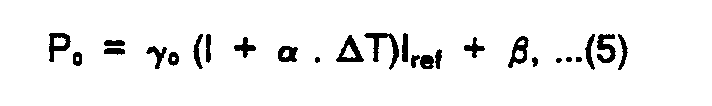
- γo is the conversion factor (in the example shown in Fig. 24, it is 4.69 mW/mA),
- a is the temperature coefficient of o (in the same example as in the above, it is -496 ppm/°C),
- AT is the deviation from the room temperature - (25°C) (in°C), and
- β is a shift term that is generated due to a decrease in the conversion efficiency when the light output is small (in the same example as in the above, it is 0.07 mW).
- Each of the above numerical examples represents the value that is obtained from the measured values when the ambient temperature is varied from 0°C to 50°C.
- As shown in the characteristics of Fig. 24, for a constant reference current Iref, the light output Po decreases with rise in the temperature. In other words, the light output Po has a negative temperature coefficient (for example, a = -496 ppm/°C).
- Therefore, the compensation for the negative temperature coefficient a for the light output Po can be accomplished by giving the reference current Iref a temperature coefficient which has the opposite sign to, and a coefficient value that corresponds to, the temperature coefficient of the light output Po.
- Namely, the reference current Iref for the case when the temperature coefficient is taken into account is given by

- Iref0 is the reference current at the room temperature (25°C),
- αi is the temperature coefficient for the reference current.
- By substituting Eq. (6) into Eq. (5) one obtains
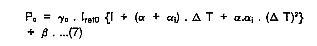


- In other words, if the temperature coefficient of the reference current is set from Eq. (8) as αi = +496 ppm/°C, the condition a . αi « I can be satisfied, and the light output Po will no longer have a temperature dependence as a result of compensation by the temperature coefficient of the reference current.
- According to the present invention, as a means of giving a temperature coefficient, as represented by αi, to the reference current Iref, a circuit is constructed by connecting a
temperature compensating circuit 18 that includes a Zener diode ZD to the variable reference current source circuit, as in the above, and made use of the temperature coefficient a of the Zener voltage Vz of the Zener diode ZD. - By choosing a Zener diode ZD which possesses a positive temperature coefficient for the temperature coefficient αz of the Zener voltage Vz, it becomes possible to give a corresponding temperature coefficient to the reference current Iref also, as may be seen from Eq. (4).
- From Eq. (4), the temperature coefficient a z of the Zener voltage and the temperature coefficient a i of the reference current are related by the following equation.

- Corresponding to the numerical values shown earlier, it becomes possible to adjust the temperature coefficient a i of the reference current to satisfy Eq. (8), by choosing the temperature coefficient α z of the Zener voltage of about +600 ppm/°C and by appropriately adjusting the values of the resistances R18 and R,,.
- Next, in Fig. 25, there is shown a modification to the fourth embodiment. This modification is realized by making it possible to set the reference current Iref that is set in a reference current source circuit J, between two kinds of reference current values, namely, Iref1 and Iref2, by switching.
- When applying the temperature compensation circuit for the light output of the laser diode to, for example, a laser light source of a laser diode, it is necessary to control the light output Po stably to the two state of different output values, namely, the read power and the write power of an optical disk drive. The present modification is an extremely preferred circuit for application to such a case.
- Regarding the configuration of the modification, that the reference current source circuit J4 has an operational amplifier A6 and a
temperature compensation circuit 18 that includes a Zener diode ZD on the input side of the operational amplifier A6, is analogous to the circuit of Fig. 23. In this modification, the output side of the operational amplifier A6 has the following configuration for setting the reference current Iref to the two values. - Namely, on the anode terminal lie side of the photodiode PD there are connected a first and a second
differential amplifiers - A first and a second
differential amplifiers differential amplifier 26a and the base of the transistor Q16 in the seconddifferential circuit 26b there is applied a switch-controlling voltage Vsfrom a controlvoltage input terminal 20. On the other hand, to the base of the transistor Q14 in the firstdifferential amplifier 26a and the base of the transistor Q,s in the seconddifferential amplifier 26b, there is applied a reference voltage Vref2 (in the example shown in the figure, it is the ground potential). - When the relation between the switch-controlling voltage Vs and the reference voltage Vref2 satisfies Vs > Vref2, the transistor Q13 in the first
differential amplifier 26a is shifted to on-state, and the anode terminal Ilc of the photodiode PD is selected to the collector current I ref1 of the transistor Q17 in the cross-coupled circuit 19. - On the other hand, when Vs < Vref2, the transistor Q15 in the second
differential amplifier 26b is shifted to on-state, and the anode terminal IIc of the photodiode PD is selected to the collector current Iref2 of the transistor Q18 in the cross-coupled circuit 19. - Now, the voltage V, at the junction between the transistor Q19 and the resistor R21 for setting the first reference current, and the voltage V2 at the junction between the transistor Q20 and the resistor R22 for setting the second reference current, are both equal to the input voltage Vc of the operational amplifier A6. Therefore, the two kinds of reference current values Iref1 and Iref2 are prescribed nearly similar to Eq. (4) by the following equations.


- The configuration other than the part of reference current source circuit J., the operation of compensating for the temperature characteristics of the light output of the laser diode LD by the temperature characteristics of the first and the second reference currents Iref1 and Iref2 that are set, the fact that the temperature coefficients of the reference currents Iref1 and I ref2 are set to the desired values by means of the temperature coefficient of the Zener voltage Vz of the Zener diode, and so on, are approximately the same as in the case of the fourth embodiment.
- Therefore, according to the present modification, it is possible to control the light output of the laser diode to the two kinds of output levels very stably, without involving temperature dependence.
- By applying this modification to an optical disk device, it is possible to simultaneously decrease temperature coefficients of read and write beams.
- Figure 26 is a diagram for showing the fifth embodiment of the present invention.
- This embodiment is obtained by adding to the driving circuit for the laser diode LD that consists of the photodiode PD, a reference current source I, an inverting and amplifying means 2 that has a junction field effect transistor (JFET) Q2, a
feedback circuit 3, and a forwardcurrent driver 4, a resetting circuit U, that consists of a detectingmeans 21 and a reset means 22. By this configuration, the power supply voltage Vcc that is supplied by a positivepower supply line 2a is monitored, and the driving circuit is reset so as to prevent the operation of the laser diode LD when the voltage Vcc is lowered to a predetermined voltage value. - Now, the reference current source I that is provided in the driving circuit actually consists of a voltage current conversion circuit that is instrumented an operational amplifier. To the noninverting input terminal of the operational amplifier, there is applied a voltage which is obtained by driving the power supply voltage +Vcc to an appropriate voltage value, as a voltage for setting reference current. On the output side of the operational amplifier, there is set a converted current that has a value that corresponds to the voltage for setting, as a reference current Iref.
- Further, the junction of the anode terminal IIc and the reference current source I is connected to the gate of a controlling transistor Q,, that consists of a JFET. The symbol R2, designates a source resistor, and the drain is connected to the base of the driving transistor Q,.
- When the power supply voltage +Vcc is kept constant at a predetermined voltage value, the difference between the photovoltaic current Isof the photodiode PD that monitors the light output of the laser diode LD and the reference current Iref that is set to the reference current source I, is inverted and amplified by the controlling transistor Q,,, and the inverted and amplified output is fed back via a forward
current circuit 4 to afeedback circuit 3. By means of the feedback action, the forward current If of the laser diode LD is controlled to a current value that corresponds to the reference current Iref, and the light output Po of the laser diode LD is controlled so as to have a fixed value on the output level that corresponds to the set reference current Iref. - Now, let the forward voltage, coresponding to the oscillating state of the laser diode when the forward current I, reached a threshold current value, be called Vf, and the base-emitter voltage of the driving transistor Q,, VBE. Next, the operation of the laser diode LD during increase in the power supply voltage V cc from OV to a predetermined value as shown in Fig. 27, which occurs in such a case as, for example, during the on-state operation of the power supply will be considered.
- When V, and V2 in Fig. 27 are fixed to

- Further, when the power supply voltage has a value in between the above two, V, < Vcc < V2, the driving transistor Q2 is capable of being shifted to an on-state by being triggered by the bias current Ib, so that forward current I, with some magnitude flows in the laser diode LD.
- On the other hand, the operational amplifier that sets the reference current Iref is desired to become inactive when the power supply voltage Vcc is less than a predetermined voltage. However, an excess output voltage may sometimes be generated due to a malfunction caused by an inversion in the balancing of the input voltages to the inverting and noninverting input terminals.
- In such a case, the reference current Iref is set at an abnormally high value, and an excess forward current I f flows in the laser diode LD based on this, generating an abnormally high light output Po.
- However, when the laser diode LD is used, for instance, as the light source for an optical disc device, if such an abnormally hight light output Po is generated, in a case such as the closing or opening of the power supply, under the generation of a state of low impressed voltage, then an erroneous writing or erasing of a signal for the recording medium will take place. The fifth embodiment shown in Fig. 26 is aimed at eliminating such a problem. In the embodiment, the laser diode LD is arranged to become inoperative in a state, such as the time of closing or opening of the power supply, when the power supply voltage is low, by means of the provision of a detecting
means 21 which detects the drop of the power supply voltage Vcc to a predetermined voltage value Vcc' that is shown in Fig. 28, and a resetting means 2 consisting of a transistor Q22 which is operated by the signal detected by the detecting means 21 to set the driving circuit to the nondriving condition. - In the above, the predetermined voltage source Vcc' has a value which is prescribed by the following conditions.


- In Fig. 26, the detecting means 21 in the resetting circuit U, of the present embodiment consists of two sets of voltage divider circuits, namely, a first
voltage divider circuit 24 formed by two resistors Rx and R26 and a secondvoltage divider circuit 23 formed by two resistors R23 and R24, and one transistor Q21. - Namely, the first and the second
voltage divider circuits power supply line 2a and the ground, with thevoltage dividing point 24a of the firstvoltage dividing circuit 24 connected to the base of the resetting transistor Qn, and the voltage dividing point 23a of the secondvoltage divider circuit 23 connected to the base of the transistor Q21. Further, the collector of the transistor Q21, is connected to the base of the resetting transistor Q22. - If the voltages between the base and the emitter of the transistors Q22 and Q21 are called VBE22 and VBE21, respectively, then the resistors in the
voltage divider circuits 

- Moreover, the resistors that appear between the first and the second
voltage divider circuits 
- Referring to Figs. 29 (A) and 29 (B), the operation of the present embodiment will be described next. Figure 29 (A) shows the changes in the rise and the fall of the power supply voltage V cc and Fig. 29 (B) shows the changes in the reset signal V r that is output from the resetting circuit U, during the rise or fall of the power supply voltage Vcc.
- First, when the power supply voltage Vcc reaches a voltage V3 in its rising, it is detected by the first
voltage divider circuit 24, and the voltage VBE22 is generated fromvoltage dividing point 24a. By the voltage VBE22, the resetting transistor Q22 is shifted to on-state, an L level reset signal Vr is output from the resetting circuit U,, and the driving transistor Q2 becomes off-state to set the driving circuit to the nondriving state. - When the voltage reaches V4 with a rise in the power supply voltage Vcc this is detected by the
second circuit 23, and a voltage of VBE21 is generated at the voltage dividing point 23a. The transistor Q21 is shifted to on-state by the voltage VBE21 which sets the resetting transistor Q22 to off-state, and an H level reset signal V is output from the resetting circuit U,. - By the H level reset signal Vr, the driving transistor Q2 is shifted to on-state, and the driving circuit returns to the driving condition.
- However, when the power supply voltage Vcc becomes Vcc', namely, V3 < Vcc' < V4, the reset signal V, becomes L level, and the driving circuit is set to the nondriving condition.
- On the other hand, during the fall of the power supply voltage Vcc, the process is opposite to what has been described in the above. First, when the power supply voltage Vcc drops to the voltage V4, the transistor Q21 is shifted to off-state, causing the resetting transistor Q22 to become on-state, and the driving circuit is set to the nondriving condition due to the outputting of an L level reset signal V,.
- When the power supply voltage Vcc drops further to the voltage V,, the resetting transistor Q22 is shifted to off-state, the reset signal Vr becomes H level. In this state, no forward current is supplied from the driving circuit since the power supply voltage V cc is excessively low.
- More specifically, by choosing the resistances in the first
voltage divider circuit 24 as R25 = 8.6 kΩ and R26 = 20 kΩ, the resistances in the secondvoltage divider circuit 23 as R23 = 22 KΩ and R24 = 10 kΩ, V, = 1.5 V and V2 = 2.2 V, and regulating V, and V4 to V, = I V and V4 = 3 V, it was found that the driving current can be reset in the prescribed range of the power supply voltage and that the malfunctions of the driving circuit can be prevented. - Figure 30 shows a first modification to the fifth embodiment. In this modification, use is made of a window comparator consisting of two differential amplifier circuits (operational amplifiers), namely, a first circuit A11 and a second circuit A12, as a detecting means in the resetting circuit U2.
- The first differential amplifier circuit A,, consists of a pair of transistors Q23 and Q24 that are biased by a constant
current source 28a, and an active load that is formed by current mirror transistors Q27 and Q28. - The second differential amplifier circuit A,2 consists of a pair of transistors Q25 and Q26 that are biased by a constant
current source 28b, with the current mirror transistors Q27 and Q28 as the common active load. -
Reference numeral 28c is a biased constant current source for the current mirror transistors Q27 and Q28, and 29 is an output terminal for the window comparator. -
Reference numeral 30 is a setting circuit for the input voltage Vi for the window comparator, and is composed of two diodes D, and D2 and three resistors R28, R29, and R32. By calling the forward voltage for each of the diodes D, and D2 as Vfd, the input voltage Vi is set as in the following equation.
- Further,
reference numeral 31 is a circuit for setting the first and the second reference voltage Vref1 and V ref2 for the first and the second differential amplifiers A,, and A12, respectively, and is composed of three diodes D3, D4, and D5 and four resistors R34. Rn, R30, and R31. The first reference voltage VRef1 is set corresponding to the power supply voltage V3, and the second reference voltage Vref2 is set corresponding to the power supply voltage V4. That is, the first and the second reference voltages Vref1 and Vref2 are set to satisfy the following relations for the first and the second power supply voltages V3 and V,.

- Figure 31 is a characteristic diagram which shows the relations represented by Eq. (17), namely, the relation between the power supply voltage Vcc and the input voltage Vi.
- The detecting means that consists of the window comparator outputs a detection signal Vd of H level from the
output terminal 29, when the input voltage Vi satisfies

- To give a concrete example, Vi' in the input
voltage setting circuit 30 was set, for exaple, to I V, and the first and the second reference voltages V ref1 and Vref2 were set to 0.5 V and 2.1 V, respectively. Accordingly, the driving circuit was set to be nondriving at a prescribed voltage value of the power supply voltage Vcc in the range between V3 = 1.5 V and V. = 3.1 V, as determined from Eq. - (17), and the malfunctions fo the driving circuit during the fall of the power supply voltage Vcc was found to be prevented. - In Fig. 32, there is shown a seond modification to the fifth embodiment. In this modification, there is included a time constant circuit that is needed, in the resetting circuit U3. This is for making the resetting operation of the driving circuit to be se- curer by continuing the generation of the reset signal Vr for a duration that is needed, when the power supply voltage Vcc underwent a rapid change of rise or fall in the closing or opening of the power supply.
- The resetting circuit U3 in the modification has resetting transistors Q29a and Q22b that are arranged side by side, the collectors of the two resetting transistors Q22a and Q22b are jointly connected, and the common joining point is connected to the base of the driving transistor Q2.
- Except for that two of the resetting transistors Q22a and Q22b are arranged side by side and that a time constant circuit is provided, the configuration is substantially the same as for the fifth embodiment shown in Fig. 26.
- First, a rise time constant circuit consisting of a capacitor C, and a resistor R36 is connected between a positive
power supply line 2a and the ground, and the output point for the rise time const signal Va is connected to the base of the resetting transistor Q22a. - On the other hand, a capacitor C2 that constitutes a fall time constant circuit is connected between the positive
power supply line 2a and the voltage dividing point 23a of the secondvoltage divider circuit 23. The fall time constant circuit consists of the capacitor C2 and two resistors R23 and R24. Further, during the fall, the power supply voltage Vcc is shifted to off-state, and there will be no charge to actuate the fall time constant circuit. Therefore, a series circuit consisting of a resistor R35 and a capacitor C3 is connected between the positivepower supply line 2a and the ground, as a charge holding circuit. - Referring to Figs. 33 (A) to 33 (H), the operation of the modification will now be described. During the rise of the power supply voltage Vcc-(Fig. 33 (A)), the rise time constant signal Va is generated for a duration t, that is prescribed by the time constant τ1 = C,.R36 of the rise time constant circuit (Fig. 33 (B)). Then, one of the resetting transistors, Q22a, is shifted to on-state and an L level reset signal Vr is output (Figs. 33 (C) and 33 - (H)). By the reset signal Vr, the driving circuit is reset for a duration of t,, and the malfunction of the driving circuit in the rise of the power supply voltage Vcc can be prevented.
- On the other hand, during the supply of the prescribed power supply voltage Vcc, there is charged the power supply voltage Vcc in the capacitor C3 of the charge holding circuit, as shown in Fig. 33(D).
- Further, during the fall of the power supply voltage Vcc(Fig. 33 (A)), there is generated a fall time constant signal Vb for a duration of t2 prescribed by the time constant τ2 = C2.(R23//R24) of the fall time constant circuit (Fig. 33 (E)), shifting the transistor Q21 to off-state. Then, the other resetting transistor Q22b becomes on-state (Figs. 33 (F) and 33 (G)), an L level reset signal similar to that for the rise time is output (Fig. 33 (H)), and the malfunction of the driving circuit during the fall of the power supply voltage Vcc can be prevented.
- Figure 34 is a circuit diagram for showing the overall configuration constructed by connecting the peripheral circuits such as an excess current
protective circuit 10, a reference current switching circuit J,, atemperature compensation circuit 18, and a resetting circuit U,, to a combination of the circuits for the first through the fifth embodiments, namely, the basic driving circuit consisting of the laser diode LD, the photodiode PD, a reference current source I, an inverting and amplifyingcircuit 2, afeedback circuit 3, and a forwardcurrent circuit 4. With such a configuration, the laser diode driving circuit is possible to control the light output from the laser diode at a predetermined value stably and fast. In addition, it is possible to protect the laser diode against an excess current, temperature changes, and fall in the power supply voltage, and to variably modulate the light output of the laser diode to the predetermined values that correspond to a plurality of reference voltages.
Claims (68)
- I. An apparatus for driving a semiconductor device which emits a light by supplying a driving current, comprising:means for outputting a photovoltaic current having a value corresponding to the intensity of the light emitted from the semiconductor device;means for supplying a reference current having a predetermined value; andmeans for controlling the driving current to be supplied to the semiconductor device so that the photovoltaic current output from the outputting means changes in proportion to the reference current from the supplying means.
- 2. The semiconductor device driving apparatus as claimed in claim I, wherein the anode of the semiconductor device and the cathode of the outputting means are connected.
- 3. The semiconductor device driving apparatus as claimed in claim I, wherein the cathode of the semiconductor device and the cathode of the outputting means are connected.
- 4. The semiconductor device driving apparatus as claimed in claim 8, wherein the current controlling means comprises a resistor for over current.
- 5. The semiconductor device driving apparatus as claimed in claim I, wherein the reference current supplying means comprises a current source.
- 6. The semiconductor device driving apparatus as claimed in claim I, wherein the reference current supplying means comprises a resistor.
- 7. The semiconductor device driving apparatus as claimed in claim I, further comprising:a switching circuit that is connected to the semiconductor device for intermittently supplying the driving current to switch-control the semiconductor device.
- 8. The semiconductor device driving apparatus as claimed in claim 7, wherein the switching circuit comprises a switching transistor.
- 9. The semiconductor device driving apparatus as claimed in claim I, further comprising:a capacitor connected in parallel to the controlling means for preventing the oscillation.
- 10. The semiconductor device driving apparatus as claimed in claim 4, wherein the voltage that is supplied to the controlling means is about + 5 V.
- II. The semiconductor device driving apparatus as claimed in claim I, further comprising:current restricting means for detecting a forward current supplied to the semiconductor device and restricting the forward current supplied to the semiconductor device, when the forward current detected by the detecting means exceeds a prescribed current value.
- 12. The semiconductor device driving apparatus as claimed in claim II, wherein the detecting means comprises a detecting resistor that is connected in series to the semiconductor device.
- 13. The semiconductor device driving apparatus as claimed in claim I, wherein the reference current supplying means comprises a reference current source for generating a plurality of reference currents, and a selecting means for selecting one of the plurality of reference currents from the reference current source.
- 14. The semiconductor device driving apparatus as claimed in claim 13, wherein the selecting means comprises a switching circuit connected between the reference current source and the controlling means.
- 15. The semiconductor device driving apparatus as claimed in claim I, wherein the reference current supplying means comprises a reference current source the temperature coefficient of the reference current has an opposite sign to the temperature coefficient of the light output and has a value that corresponds to the temperature coefficient of the light output.
- 16. The semiconductor device driving apparatus as claimed in claim 15, wherein the reference signal source comprises a constant voltage diode that has a temperature coefficient which is opposite to the temperature coefficient of light output level, and a reference signal formation circuit for forms a reference signal in response to the constant voltage from the constant voltage diode.
- 17. The semiconductor device driving apparatus as claimed in claim 4, further comprising:resetting means for detecting that the voltage of the controlling means is at least one prescribed voltage value, in order to set the forward current circuit to nondriving condition.
- 18. The semiconductor device driving apparatus as claimed in claim 17, wherein the prescribed voltage value is a first potential and a second potential.
- 19. The semiconductor device driving apparatus as claimed in claim 17, wherein the detecting means comprises of a first voltage dividing circuit formed by two resistors and a second voltage dividing circuit formed by two resistors, for dividing the power supply voltage, and a transistor connected between the first and the second voltage dividing circuits.
- 20. The semiconductor device driving apparatus as claimed in claim I, wherein the current controlling means comprises a transistor.
- 21. The semiconductor device driving apparatus as claimed in claim 20, wherein the driving current is supplied from the collector of the transistor to the semiconductor device.
- 22. The semiconductor device driving apparatus as claimed in claimed in claim 20, wherein the driving current is supplied from the emitter of the translater to the semiconductor device.
- 23. An apparatus for driving a semiconductor device which emits a light by supplying a driving current, comprising:means for outputting a photovoltaic current having a value corresponding to the intensity of the light emitted from the semiconductor device;means for supplying a reference curent having a predetermined value; andmeans for controlling the driving current to be supplied to the semiconductor device so that the photovoltaic current output from the outputting means changes in proportion to the reference current from the supplying means, the current controlling means comprising a voltage comparator for inverting and amplifying the difference current between the photovoltaic current from the light detecting means and the reference current from the reference current supplying means, and a feedback circuit for controlling the forward current to a current value that corresponds to the reference current, by feeding back the inverted and amplified output from the voltage comparator to the semiconductor device.
- 24. A semiconductor device driving circuit comprising:means for supplying a driving current to the semiconductor device which emits a light corresponding to the supplied driving current;means for generating a photovoltaic current in response to the intensity of the light emitted from the semiconductor device;means for outputting a reference current having a predetermined current value; andmeans for controlling and supplying means so that the photovoltaic current output from the outputting means changes in proportion to the reference current.
- 25. The semiconductor device driving circuit as claimed in claim 24, wherein the anode of the semiconductor device and the cathode of the photodiode are connected.
- 26. The semiconductor device driving means as claimed in claim 24, wherein the cathode of the semiconductor device and the cathode of the photodiode are connected.
- 27. The semiconductor device driving circuit as claimed in claim 24, wherein said controlling means comprises a resistor for overcurrent.
- 28. The semiconductor device driving circuit as claimed in claim 24, wherein the reference current outputting means comprises a current source.
- 29. The semiconductor device driving circuit as claimed in claim 24, wherein the reference current outputting means comprises a resistor.
- 30. The semiconductor device driving circuit as claimed in claim 24, further comprising:a switching circuit that is connected to the semiconductor device for intermittently supplying the driving current to switching-control the semiconductor device.
- 31. The semiconductor device driving circuit as claimed in claim 30, wherein the switching circuit comprises a switching transistor.
- 32. The semiconductor device driving circuit as claimed in claim 24, further comprising:a capacitor connected in parallel to the driving current controlling means for preventing the oscillation.
- 33. The semiconductor device driving circuit as claimed in claim 24, wherein the voltage that is provided to the power supply voltage terminal is about + 5 V.
- 34. The semiconductor device driving circuit as claimed in claim 24, wherein the reference current outputting means comprises a current source of which temperature coefficient has a sign which is opposite to that of the light output and has a value that corresponds to the temperature coefficient of the light output.
- 35. The semiconductor device driving circuit as claimed in claim 34, wherein the reference current source comprises a reference signal formation circuit for forms a reference signal in response to the constant voltage from the constant voltage diode which has a temperature coefficient which is op- pocite to the temperature coefficient of light output level.
- 36. The semiconductor device driving circuit as claimed in claim 24, further comprising:resetting means for detecting that the voltage of the controlling means is at least one prescribed voltage value, in order to set the forward current circuit to nondriving condition.
- 37. The semiconductor device driving circuit as claimed in claim 36, wherein the prescribed voltage value is a value that lies between a first potential and s second potential.
- 38. The semiconductor device driving circuit as claimed in claim 36, wherein the detecting means comprises of a first voltage dividing circuit formed by two resistors and a second voltage dividing circuit formed by two resistors, for dividing the power supply voltage, and a transistor connected between the first and the second voltage dividing circuits.
- 39. The semiconductor device driving circuit as claimed in claim 24, wherein the current controlling means comprises a transistor.
- 40. The semiconductor device driving circuit as claimed in claim 40, wherein the supplying means is controlled by the collector of the transistor.
- 41. The semiconductor device driving circuit as claimed in claimed in claim 39, wherein the driving current supply means comprises a resistor.
- 42. The semiconductor device driving circuit as claimed in claim 24, wherein said drive current supplying means comprises a transistor.
- 43. A circuit adapted for driving a first semiconductor device for emitting light by supplying a driving current, comprising:a first circuit having a first terminal to supply the driving current to the first semiconductor device; anda second circuit having a second terminal to receive a control current from a second semiconductor device for detecting light, and a third terminal to receive a reference current, the second circuit is connected to the first circuit and controls the driving current to be supplied to the first terminal so that the control current changes in proportion to the reference current.
- 44. The first semiconductor device driving circuit as claimed in claim 43, wherein the first circuit further has a current protective resister connected in series to the first semiconductor device.
- 45. The semiconductor device driving circuit as claimed in claim 43, wherein reference curent sup- plyed to the third terminal of the second circuit is from a current source.
- 46. The semiconductor device driving circuit as claimed in claim 43, wherein the reference current is a resistor.
- 47. The semiconductor device driving circuit as claimed in claim 43, further comprising:a switching transistor which is connected in parallel to the semiconductor device for switching the first semiconductor device.
- 48. The semiconductor device driving circuit as claimed in claim 43, further comprising:a capacitor connected in parallel to the first circuit for preventing the oscillation.
- 49. The semiconductor device driving circuit as claimed in claim 43, wherein the voltage that is supplied to the first circuit or second circuit is about + 5 V.
- 50. The semiconductor device driving circuit as claimed in claim 43, further comprising:current restricting means for detecting a forward current supplied to the semiconductor device and for restricting the forward current supplied to thesemiconductor device, when the forward current detected by the detecting means exceeds a prescribed current value.
- 51. The semiconductor device driving circuit as claimed in claim 50, wherein the detecting means comprises a detecting resistor that is connected in series to the semiconductor device.
- 52. The semiconductor device driving circuit as claimed in claim 43, wherein the second circuit has a reference current source the temperature coefficient of the reference current being set by the current source has a sign which is opposite to the temperature coefficient of the light output and has a value that corresponds to the temperature coefficient of the light output.
- 53. The semiconductor device driving circuit as claimed in claim 52, wherein the reference signal source comprises a constant voltage diode that has a temperature coefficient which is opposite to the temperature coefficient of light output level, and a reference signal formation circuit for forms a reference signal in response to the constant voltage from the constant voltage diode.
- 54. The semiconductor device driving circuit as claimed in claim 43, further comprising:resetting means for detecting that the voltage of the controlling means is at least one prescribed voltage value, in order to set the forward current circuit to nondriving condition.
- 55. The semiconductor device driving circuit as claimed in claim 54, wherein the prescribed voltage value is a value that lies between a first potential and a second potential.
- 56. The semiconductor device driving circuit as claimed in claim 54, wherein the detecting means comprises of a first voltage dividing circuit formed by two resistors and a second voltage dividing circuit formed by two resistors, for dividing the power supply voltage, and a transistor connected between the first and the second voltage dividing circuits.
- 57. The semiconductor device driving apparatus as claimed in claim 43, wherein the second circuit comprises a transistor.
- 58. The semiconductor device driving apparatus as claimed in claim 43, wherein the driving current is supplied from the collector of the transistor to the semiconductor device.
- 59. The semiconductor device driving apparatus as claimed in claimed in claim 43, wherein the first circuit comprises a transistor.
- 60. An apparatus for driving a semiconductor device which emits a light by supplying a driving current, comprising:means for outputting a photovoltaic current having a value corresponding to the intensity of the light emitted from the semiconductor device;means for supplying a reference voltage having a predetermined value;means for comparing the reference voltage supplied from the supplying means with a voltage having a value in accordance with the photovoltaic current output from the outputting means, and for generating a control signal coresponding to the comparison by the comparing means; andmeans for controlling semiconductor device in response to the control signal generated from the comparing means.
- 61. The semiconductor device driving apparatus as claimed in claim 60, wherein the anode of the semiconductor device and the cathode of the photodiode are connected.
- 62. The semiconductor device driving apparatus as claimed in claim 60, wherein the cathode of the semiconductor device and the cathode of the photodiode are connected.
- 63. The semiconductor device driving apparatus as claimed in claim 60, wherein the semiconductor device controlling means comprises a current protective resistor which is connected in series to the semiconductor device.
- 64. The semiconductor device driving apparatus as claimed in claim 60, wherein the reference voltage supplying means comprises a current source.
- 65. The semiconductor device driving apparatus as claimed in claim 60, wherein the reference voltage supplying means comprises a resistor.
- 66. The semiconductor device driving apparatus as claimed in claim 60, further comprising:a capacitor for preventing the oscillation.
- 67. The semiconductor device driving apparatus as claimed in claim 60, wherein the reference voltage supplying means comprises a reference current source for generating a plurality of reference currents, and a selecting means for selecting one of the plurality of reference currents from the reference current source.
- 68. The semiconductor device driving apparatus as claimed in claim 67, wherein the selecting means comprises a switching circuit connected between the reference current source and the inverting and amplifying means.
Applications Claiming Priority (10)
| Application Number | Priority Date | Filing Date | Title |
|---|---|---|---|
| JP60179255A JPS6240789A (en) | 1985-08-16 | 1985-08-16 | Laser diode driving circuit |
| JP179255/85 | 1985-08-16 | ||
| JP184042/85 | 1985-08-23 | ||
| JP60184042A JPS6245191A (en) | 1985-08-23 | 1985-08-23 | Optical output controlling curcuit for laser diode |
| JP184041/85 | 1985-08-23 | ||
| JP60184041A JPS6245190A (en) | 1985-08-23 | 1985-08-23 | Circuit for protecting against excessive current for laser diode |
| JP204417/85 | 1985-09-18 | ||
| JP60204417A JPS6265531A (en) | 1985-09-18 | 1985-09-18 | Temperature characteristic compensation circuit for optical output of laser diode |
| JP60240411A JPS62102576A (en) | 1985-10-29 | 1985-10-29 | Resetting circuit for laser diode driving circuit |
| JP240411/85 | 1985-10-29 |
Publications (2)
| Publication Number | Publication Date |
|---|---|
| EP0215311A2 true EP0215311A2 (en) | 1987-03-25 |
| EP0215311A3 EP0215311A3 (en) | 1989-05-03 |
Family
ID=27528746
Family Applications (1)
| Application Number | Title | Priority Date | Filing Date |
|---|---|---|---|
| EP86111421A Withdrawn EP0215311A3 (en) | 1985-08-16 | 1986-08-18 | Laser diode driving circuit |
Country Status (3)
| Country | Link |
|---|---|
| US (1) | US4819241A (en) |
| EP (1) | EP0215311A3 (en) |
| KR (1) | KR910002238B1 (en) |
Cited By (10)
| Publication number | Priority date | Publication date | Assignee | Title |
|---|---|---|---|---|
| EP0224185A2 (en) * | 1985-11-19 | 1987-06-03 | Kabushiki Kaisha Toshiba | Laser diode driving circuit |
| DE3726244A1 (en) * | 1987-08-07 | 1989-02-16 | Kabelmetal Electro Gmbh | Circuit arrangement for monitoring the power of a laser diode |
| DE3939309A1 (en) * | 1988-11-28 | 1990-05-31 | Minolta Camera Kk | Laser-beam generating structural unit with current converter - consists of switched resistances parallel to constant voltage source for optimal loading of photo diode detector |
| AU609668B2 (en) * | 1986-09-12 | 1991-05-02 | N.V. Philips Gloeilampenfabrieken | Method of and device for pulse-mode driving a semiconductor laser |
| GB2208962B (en) * | 1987-08-19 | 1991-05-08 | Plessey Co Plc | Power supply |
| EP0756363A2 (en) * | 1995-07-28 | 1997-01-29 | AT&T Corp. | Method and apparatus for monitoring performance of a laser transmitter |
| WO2007022040A1 (en) * | 2005-08-15 | 2007-02-22 | Honeywell International Inc. | Vcsel pin sensor |
| EP1772798A1 (en) * | 2005-09-13 | 2007-04-11 | Higher Way Electronic Co., Ltd. | Optical output system with auto optical power control for optical mouse |
| CN106340799A (en) * | 2016-03-10 | 2017-01-18 | 北京国科欣翼科技有限公司 | Laser device control system |
| CN106340800A (en) * | 2016-03-10 | 2017-01-18 | 北京国科欣翼科技有限公司 | Laser device |
Families Citing this family (34)
| Publication number | Priority date | Publication date | Assignee | Title |
|---|---|---|---|---|
| DE3940205B4 (en) * | 1988-12-05 | 2007-09-13 | Ricoh Co., Ltd. | Semiconductor laser controller |
| US4924473A (en) * | 1989-03-28 | 1990-05-08 | Raynet Corporation | Laser diode protection circuit |
| US5018154A (en) * | 1989-09-12 | 1991-05-21 | Brother Kogyo Kabushiki Kaisha | Semiconductor laser drive device |
| JPH07174629A (en) * | 1993-12-20 | 1995-07-14 | Mitsubishi Electric Corp | Optical degradation-detecting circuit |
| IT1268070B1 (en) * | 1994-06-06 | 1997-02-20 | Cselt Centro Studi Lab Telecom | CIRCUIT IN CMOS TECHNOLOGY FOR HIGH SPEED PILOTING OF OPTICAL SOURCES. |
| US5438581A (en) * | 1994-08-16 | 1995-08-01 | Eastman Kodak Company | Laser driver ASIC chip |
| WO1996020521A1 (en) * | 1994-12-23 | 1996-07-04 | Philips Electronics N.V. | Laser power supply circuit as well as optical recording and/or reading device comprising such a laser power supply circuit |
| JPH08204270A (en) * | 1995-01-20 | 1996-08-09 | Brother Ind Ltd | Semiconductor laser driving circuit |
| DE69627922T2 (en) * | 1995-03-24 | 2004-03-11 | Nohmi Bosai Ltd. | Sensor for the detection of fine particles such as smoke |
| US5936986A (en) * | 1996-07-30 | 1999-08-10 | Bayer Corporation | Methods and apparatus for driving a laser diode |
| US5949085A (en) * | 1997-01-29 | 1999-09-07 | Xircom, Inc. | Ratiometric compensated optical isolation coupler |
| JPH11121851A (en) * | 1997-10-15 | 1999-04-30 | Fujitsu Ltd | Light emitting device drive circuit and light emitting apparatus equipped therewith |
| US6229833B1 (en) * | 1997-10-16 | 2001-05-08 | Fujitsu Limited | Laser diode protecting circuit and laser driving current control circuit |
| JP3389480B2 (en) * | 1997-10-16 | 2003-03-24 | 富士通株式会社 | LD protection circuit |
| US6265857B1 (en) | 1998-12-22 | 2001-07-24 | International Business Machines Corporation | Constant current source circuit with variable temperature compensation |
| US6278476B1 (en) * | 2000-03-09 | 2001-08-21 | Toshiba Tec Kabushiki Kaisha | Image forming apparatus in which a laser beam is applied from a semiconductor laser to scan an image carrier, and method of controlling the apparatus |
| US6728494B2 (en) * | 2000-06-08 | 2004-04-27 | Matsushita Electric Industrial Co., Ltd. | Light-emitting device drive circuit, and optical transmission system using the circuit |
| US6496526B1 (en) * | 2000-10-18 | 2002-12-17 | Xerox Corporation | Current switching driver with controlled bias and ON states |
| JP2002261381A (en) * | 2001-02-28 | 2002-09-13 | Hamamatsu Photonics Kk | Drive current supply circuit |
| US6696887B2 (en) * | 2001-09-27 | 2004-02-24 | Matthew S. Taubman | Transistor-based interface circuitry |
| JP2003174227A (en) * | 2001-12-06 | 2003-06-20 | Mitsubishi Electric Corp | Semiconductor laser module |
| US6941080B2 (en) | 2002-07-15 | 2005-09-06 | Triquint Technology Holding Co. | Method and apparatus for directly modulating a laser diode using multi-stage driver circuitry |
| GB2393034B (en) * | 2002-09-12 | 2007-01-17 | Ericsson Telefon Ab L M | Laser driver control circuit |
| JP4581345B2 (en) * | 2003-08-08 | 2010-11-17 | 富士ゼロックス株式会社 | Light emitting element driving device and image forming apparatus |
| US7372882B2 (en) * | 2004-04-28 | 2008-05-13 | Renesas Technology Corp. | Driving circuit for and semiconductor device for driving laser diode |
| KR20060002239A (en) * | 2004-07-01 | 2006-01-09 | 삼성전자주식회사 | Apparatus for controlling laser output |
| US7512163B2 (en) * | 2005-10-04 | 2009-03-31 | Microsoft Corporation | Dual current control for laser diode driver circuit |
| GB2441007B (en) * | 2006-08-17 | 2011-08-24 | Susan Jane Branch | Auricular therapy |
| JP2009026789A (en) * | 2007-07-17 | 2009-02-05 | Nec Corp | Optical module, host board, and manufacturing method of host board |
| US8369191B2 (en) | 2010-11-29 | 2013-02-05 | Tdk Corporation | Method for controlling the current of laser diode on thermally assisted magnetic recording head |
| JP6275322B2 (en) * | 2015-02-23 | 2018-02-07 | 三菱電機株式会社 | Optical receiver |
| KR102423938B1 (en) | 2018-04-02 | 2022-07-25 | 한국전자통신연구원 | Optical network unit for optical transmission in burst mode |
| CN109286126A (en) * | 2018-11-29 | 2019-01-29 | Oppo广东移动通信有限公司 | Output control method and electronic equipment, the computer readable storage medium of laser |
| US10914627B2 (en) * | 2019-02-13 | 2021-02-09 | Semtech Corporation | Configurable laser monitor photodiode in optical modulation amplitude controller |
Citations (2)
| Publication number | Priority date | Publication date | Assignee | Title |
|---|---|---|---|---|
| JPS5861691A (en) * | 1981-10-07 | 1983-04-12 | Sharp Corp | Drive circuit for semiconductor laser |
| JPS58200444A (en) * | 1982-05-18 | 1983-11-22 | Foster Denki Kk | Light output controlling circuit |
Family Cites Families (4)
| Publication number | Priority date | Publication date | Assignee | Title |
|---|---|---|---|---|
| US3898583A (en) * | 1972-03-29 | 1975-08-05 | Xerox Corp | Laser stabilization technique |
| US4009385A (en) * | 1976-03-22 | 1977-02-22 | Bell Telephone Laboratories, Incorporated | Laser control circuit |
| JPS5624991A (en) * | 1979-08-08 | 1981-03-10 | Tech Res & Dev Inst Of Japan Def Agency | Driving circuit for pulse laser diode |
| JPS57162479A (en) * | 1981-03-31 | 1982-10-06 | Toshiba Corp | Semiconductor laser diode driving circuit |
-
1986
- 1986-08-15 US US06/897,051 patent/US4819241A/en not_active Expired - Lifetime
- 1986-08-16 KR KR1019860006763A patent/KR910002238B1/en not_active IP Right Cessation
- 1986-08-18 EP EP86111421A patent/EP0215311A3/en not_active Withdrawn
Patent Citations (2)
| Publication number | Priority date | Publication date | Assignee | Title |
|---|---|---|---|---|
| JPS5861691A (en) * | 1981-10-07 | 1983-04-12 | Sharp Corp | Drive circuit for semiconductor laser |
| JPS58200444A (en) * | 1982-05-18 | 1983-11-22 | Foster Denki Kk | Light output controlling circuit |
Non-Patent Citations (3)
| Title |
|---|
| PATENT ABSTRACTS OF JAPAN, vol. 7, no. 154 (E-185)[1299], 6th July 1983; & JP-A-58 061 691 (SHARP K.K.) 12-04-1983 * |
| PATENT ABSTRACTS OF JAPAN, vol. 8, no. 51 (P-259)[1488], 8 March 1984; & JP-A-58 200 444 (FUOSUTAA DENKI K.K.) 22-11-1983 * |
| TECHNISCHES MESSEN T.M., vol. 50, no. 2, February 1983, pages 49-54, München, DE; W.S. LUDOLF: "Grundlagen der optischen Übertragungstechnik - Eine Einführung für Anwender - Teil 6. Elektronische Systemkomponenten: Treiberstufen für optische Sender" * |
Cited By (13)
| Publication number | Priority date | Publication date | Assignee | Title |
|---|---|---|---|---|
| EP0224185A2 (en) * | 1985-11-19 | 1987-06-03 | Kabushiki Kaisha Toshiba | Laser diode driving circuit |
| EP0224185A3 (en) * | 1985-11-19 | 1989-04-26 | Kabushiki Kaisha Toshiba | Laser diode driving circuit |
| AU609668B2 (en) * | 1986-09-12 | 1991-05-02 | N.V. Philips Gloeilampenfabrieken | Method of and device for pulse-mode driving a semiconductor laser |
| DE3726244A1 (en) * | 1987-08-07 | 1989-02-16 | Kabelmetal Electro Gmbh | Circuit arrangement for monitoring the power of a laser diode |
| GB2208962B (en) * | 1987-08-19 | 1991-05-08 | Plessey Co Plc | Power supply |
| DE3939309A1 (en) * | 1988-11-28 | 1990-05-31 | Minolta Camera Kk | Laser-beam generating structural unit with current converter - consists of switched resistances parallel to constant voltage source for optimal loading of photo diode detector |
| EP0756363A2 (en) * | 1995-07-28 | 1997-01-29 | AT&T Corp. | Method and apparatus for monitoring performance of a laser transmitter |
| EP0756363A3 (en) * | 1995-07-28 | 1997-11-19 | AT&T Corp. | Method and apparatus for monitoring performance of a laser transmitter |
| WO2007022040A1 (en) * | 2005-08-15 | 2007-02-22 | Honeywell International Inc. | Vcsel pin sensor |
| EP1772798A1 (en) * | 2005-09-13 | 2007-04-11 | Higher Way Electronic Co., Ltd. | Optical output system with auto optical power control for optical mouse |
| CN106340799A (en) * | 2016-03-10 | 2017-01-18 | 北京国科欣翼科技有限公司 | Laser device control system |
| CN106340800A (en) * | 2016-03-10 | 2017-01-18 | 北京国科欣翼科技有限公司 | Laser device |
| CN106340800B (en) * | 2016-03-10 | 2019-03-12 | 北京国科欣翼科技有限公司 | Laser |
Also Published As
| Publication number | Publication date |
|---|---|
| KR870002676A (en) | 1987-04-06 |
| EP0215311A3 (en) | 1989-05-03 |
| US4819241A (en) | 1989-04-04 |
| KR910002238B1 (en) | 1991-04-08 |
Similar Documents
| Publication | Publication Date | Title |
|---|---|---|
| US4819241A (en) | Laser diode driving circuit | |
| US6362910B1 (en) | Optical transmitter having temperature compensating function and optical transmission system | |
| US7061950B2 (en) | Drive circuit and drive method of semiconductor laser module provided with electro-absorption type optical modulator | |
| US5761230A (en) | Laser-diode driving circuit with temperature compensation | |
| US5974064A (en) | Temperature compensation of laser diodes | |
| CA1085462A (en) | Automatic bias control circuit for injection lasers | |
| CA2284259C (en) | Laser modulation control method and apparatus | |
| EP0840467B1 (en) | Light emitting device drive circuit | |
| US4484331A (en) | Regulator for bias current of semiconductor laser diode | |
| US6466595B2 (en) | Laser diode driving method and circuit which provides an automatic power control capable of shortening the start-up period | |
| US5646763A (en) | Optical transmitter and laser diode module for use in the optical transmitter | |
| JP3320900B2 (en) | Automatic temperature control circuit for laser diode and electric / optical signal conversion unit using the same | |
| JP2006013252A (en) | Method and circuit for controlling laser diode, and optical transmitter | |
| EP0476719B1 (en) | A control circuit for a laser printer | |
| JP3423115B2 (en) | Optical signal transmission device | |
| US5515392A (en) | Laser diode control circuit with power supply compensation network | |
| US5881081A (en) | Automatic laser power control circuit | |
| US5107362A (en) | Optical transmission apparatus | |
| JPH11121851A (en) | Light emitting device drive circuit and light emitting apparatus equipped therewith | |
| JP3387336B2 (en) | Optical transmitter | |
| JPS61224385A (en) | Semiconductor laser drive circuit | |
| JP2573426B2 (en) | Burst type optical communication circuit | |
| JPS63289978A (en) | Circuit for laser detecting deterioration of semiconductor laser | |
| JP2746401B2 (en) | Semiconductor laser controller | |
| JP2710974B2 (en) | Optical transmitter |
Legal Events
| Date | Code | Title | Description |
|---|---|---|---|
| PUAI | Public reference made under article 153(3) epc to a published international application that has entered the european phase |
Free format text: ORIGINAL CODE: 0009012 |
|
| 17P | Request for examination filed |
Effective date: 19860818 |
|
| AK | Designated contracting states |
Kind code of ref document: A2 Designated state(s): DE FR GB NL |
|
| PUAL | Search report despatched |
Free format text: ORIGINAL CODE: 0009013 |
|
| AK | Designated contracting states |
Kind code of ref document: A3 Designated state(s): DE FR GB NL |
|
| 17Q | First examination report despatched |
Effective date: 19910128 |
|
| STAA | Information on the status of an ep patent application or granted ep patent |
Free format text: STATUS: THE APPLICATION IS DEEMED TO BE WITHDRAWN |
|
| 18D | Application deemed to be withdrawn |
Effective date: 19920610 |
|
| RIN1 | Information on inventor provided before grant (corrected) |
Inventor name: KATSUMI, NAGANO |