EP0213974A1 - Mikromodul mit eingebetteten Kontakten und Karte mit solchen Mikromodulschaltungen - Google Patents
Mikromodul mit eingebetteten Kontakten und Karte mit solchen Mikromodulschaltungen Download PDFInfo
- Publication number
- EP0213974A1 EP0213974A1 EP86401296A EP86401296A EP0213974A1 EP 0213974 A1 EP0213974 A1 EP 0213974A1 EP 86401296 A EP86401296 A EP 86401296A EP 86401296 A EP86401296 A EP 86401296A EP 0213974 A1 EP0213974 A1 EP 0213974A1
- Authority
- EP
- European Patent Office
- Prior art keywords
- micromodule
- conductive
- microcircuit
- parts
- support
- Prior art date
- Legal status (The legal status is an assumption and is not a legal conclusion. Google has not performed a legal analysis and makes no representation as to the accuracy of the status listed.)
- Granted
Links
Images
Classifications
-
- G—PHYSICS
- G06—COMPUTING OR CALCULATING; COUNTING
- G06K—GRAPHICAL DATA READING; PRESENTATION OF DATA; RECORD CARRIERS; HANDLING RECORD CARRIERS
- G06K19/00—Record carriers for use with machines and with at least a part designed to carry digital markings
- G06K19/06—Record carriers for use with machines and with at least a part designed to carry digital markings characterised by the kind of the digital marking, e.g. shape, nature, code
- G06K19/067—Record carriers with conductive marks, printed circuits or semiconductor circuit elements, e.g. credit or identity cards also with resonating or responding marks without active components
- G06K19/07—Record carriers with conductive marks, printed circuits or semiconductor circuit elements, e.g. credit or identity cards also with resonating or responding marks without active components with integrated circuit chips
- G06K19/077—Constructional details, e.g. mounting of circuits in the carrier
- G06K19/07745—Mounting details of integrated circuit chips
- G06K19/07747—Mounting details of integrated circuit chips at least one of the integrated circuit chips being mounted as a module
-
- G—PHYSICS
- G06—COMPUTING OR CALCULATING; COUNTING
- G06K—GRAPHICAL DATA READING; PRESENTATION OF DATA; RECORD CARRIERS; HANDLING RECORD CARRIERS
- G06K19/00—Record carriers for use with machines and with at least a part designed to carry digital markings
- G06K19/06—Record carriers for use with machines and with at least a part designed to carry digital markings characterised by the kind of the digital marking, e.g. shape, nature, code
- G06K19/067—Record carriers with conductive marks, printed circuits or semiconductor circuit elements, e.g. credit or identity cards also with resonating or responding marks without active components
- G06K19/07—Record carriers with conductive marks, printed circuits or semiconductor circuit elements, e.g. credit or identity cards also with resonating or responding marks without active components with integrated circuit chips
- G06K19/077—Constructional details, e.g. mounting of circuits in the carrier
- G06K19/07745—Mounting details of integrated circuit chips
-
- H—ELECTRICITY
- H10—SEMICONDUCTOR DEVICES; ELECTRIC SOLID-STATE DEVICES NOT OTHERWISE PROVIDED FOR
- H10W—GENERIC PACKAGES, INTERCONNECTIONS, CONNECTORS OR OTHER CONSTRUCTIONAL DETAILS OF DEVICES COVERED BY CLASS H10
- H10W70/00—Package substrates; Interposers; Redistribution layers [RDL]
- H10W70/60—Insulating or insulated package substrates; Interposers; Redistribution layers
- H10W70/611—Insulating or insulated package substrates; Interposers; Redistribution layers for connecting multiple chips together
-
- H—ELECTRICITY
- H10—SEMICONDUCTOR DEVICES; ELECTRIC SOLID-STATE DEVICES NOT OTHERWISE PROVIDED FOR
- H10W—GENERIC PACKAGES, INTERCONNECTIONS, CONNECTORS OR OTHER CONSTRUCTIONAL DETAILS OF DEVICES COVERED BY CLASS H10
- H10W70/00—Package substrates; Interposers; Redistribution layers [RDL]
- H10W70/60—Insulating or insulated package substrates; Interposers; Redistribution layers
- H10W70/62—Insulating or insulated package substrates; Interposers; Redistribution layers characterised by their interconnections
- H10W70/63—Vias, e.g. via plugs
- H10W70/635—Through-vias
-
- H—ELECTRICITY
- H10—SEMICONDUCTOR DEVICES; ELECTRIC SOLID-STATE DEVICES NOT OTHERWISE PROVIDED FOR
- H10W—GENERIC PACKAGES, INTERCONNECTIONS, CONNECTORS OR OTHER CONSTRUCTIONAL DETAILS OF DEVICES COVERED BY CLASS H10
- H10W70/00—Package substrates; Interposers; Redistribution layers [RDL]
- H10W70/60—Insulating or insulated package substrates; Interposers; Redistribution layers
- H10W70/699—Insulating or insulated package substrates; Interposers; Redistribution layers for flat cards, e.g. credit cards
-
- H—ELECTRICITY
- H10—SEMICONDUCTOR DEVICES; ELECTRIC SOLID-STATE DEVICES NOT OTHERWISE PROVIDED FOR
- H10W—GENERIC PACKAGES, INTERCONNECTIONS, CONNECTORS OR OTHER CONSTRUCTIONAL DETAILS OF DEVICES COVERED BY CLASS H10
- H10W72/00—Interconnections or connectors in packages
- H10W72/50—Bond wires
- H10W72/531—Shapes of wire connectors
- H10W72/5363—Shapes of wire connectors the connected ends being wedge-shaped
-
- H—ELECTRICITY
- H10—SEMICONDUCTOR DEVICES; ELECTRIC SOLID-STATE DEVICES NOT OTHERWISE PROVIDED FOR
- H10W—GENERIC PACKAGES, INTERCONNECTIONS, CONNECTORS OR OTHER CONSTRUCTIONAL DETAILS OF DEVICES COVERED BY CLASS H10
- H10W72/00—Interconnections or connectors in packages
- H10W72/851—Dispositions of multiple connectors or interconnections
- H10W72/874—On different surfaces
- H10W72/884—Die-attach connectors and bond wires
-
- H—ELECTRICITY
- H10—SEMICONDUCTOR DEVICES; ELECTRIC SOLID-STATE DEVICES NOT OTHERWISE PROVIDED FOR
- H10W—GENERIC PACKAGES, INTERCONNECTIONS, CONNECTORS OR OTHER CONSTRUCTIONAL DETAILS OF DEVICES COVERED BY CLASS H10
- H10W74/00—Encapsulations, e.g. protective coatings
-
- H—ELECTRICITY
- H10—SEMICONDUCTOR DEVICES; ELECTRIC SOLID-STATE DEVICES NOT OTHERWISE PROVIDED FOR
- H10W—GENERIC PACKAGES, INTERCONNECTIONS, CONNECTORS OR OTHER CONSTRUCTIONAL DETAILS OF DEVICES COVERED BY CLASS H10
- H10W90/00—Package configurations
- H10W90/701—Package configurations characterised by the relative positions of pads or connectors relative to package parts
- H10W90/751—Package configurations characterised by the relative positions of pads or connectors relative to package parts of bond wires
- H10W90/754—Package configurations characterised by the relative positions of pads or connectors relative to package parts of bond wires between a chip and a stacked insulating package substrate, interposer or RDL
Definitions
- the present invention relates to a micromodule with buried contacts. It also relates to a CCC type card containing circuits comprising such a micromodule. It finds application in the fields of electronic payment or security.
- CCC a special card containing an electronic microcircuit.
- the microcircuit can consist of a writable memory, a read only memory and up to a microcomputer in the case of high level CCC cards. It is known to constitute the CCC card in at least two parts. The first part consists of the plastic card itself. A second part consists of a micromodule comprising a support, electrical contacts and at least one microcircuit connected to said contacts and fixed to the support.
- micromodule of the prior art described therein comprises a substrate, lateral and central conductive areas formed on the external face of the substrate.
- the arrangement described has drawbacks. Indeed, once the micromodule installed on the plastic card proper, according to this state of the art, the microcircuit installed on the substrate is invisible from the outside. Also found from the outside to the inside of the card first of all the conductive parts constituting in particular the contacts, a substrate for example of PVC type then the microcircuit connected by wires to the lateral conductive areas.
- a well dug inside the PVC substrate allows to stick the microcircuit on the internal face of the central conductive part.
- the connecting wires of the microcircuit are arranged inside transverse perforations of the substrate and fixed on the lateral conductive pads.
- Such cards are subject to risks of deterioration of the metal parts. Indeed, it will be noted that the dimensions of the card are very small.
- the metallic film is of the order of 60 microns thick.
- the card is inserted into a reader.
- the contacts are connected to the reader by a friction connector. When removing the card, the contacts being hot, there is a risk of damage to the contacts.
- Another drawback of this arrangement is that the card is intended to be handled in sometimes extreme conditions.
- the card can be bent, which constitutes a risk of detachment of the metal parts.
- the invention proposes a micromodule, the conductive parts of which are arranged on the internal face of a plastic support.
- a microcircuit is placed on the internal face of a central conductive part and wires for connection of this microcircuit to lateral conductive parts are provided. Perforations in the plastic support allow contact areas to be formed in predetermined locations.
- the invention also makes it possible to avoid drilling a central well in the plastic support to house the microcircuit on the internal face of the central metal.
- the invention also relates to a card containing a circuit comprising a micromodule according to the invention arranged on a plastic card.
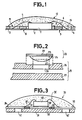
- FIG. 1 there is shown a micromodule formed according to the prior art.
- a microcircuit 1 is placed on a metallic film 2.
- the metallic film is initially formed by an etched strip so as to arrange a central part 2 which receives the microcircuit 1 and lateral parts 3, 4, which will receive the ends of connections 5, 6 of the chip.
- the metal strip 2 - 4 is bonded to the external face of a plastic film constituting a material support for the micromodule.
- This plastic film is pierced with two kinds of holes.
- a first kind of hole is constituted by a hole 7 or well in which the microcircuit 1 is placed.
- This well is compulsory in this method of the prior art to provide a rear connection of the microcircuit. This is particularly the case for microcircuits with substrate polarization, in particular silicon.
- Another kind of drilling is constituted by the holes 10 and 11 which make it possible to bring the connection wires 6 and 5 to the lateral conductive parts 3 and 4.
- the conductive wires 5, 6 are fixed by welding or gluing on the internal face of the conductive strip.
- the internal face of the micromodule, upper in the drawing is embedded in a bead of protective resin 12 deposited hot.
- FIG. 2 there is shown the inserting operation of the micromodule.
- the micromodule 20 consisting of the conductive parts of external contact 22, of the support 23 and of the drop of resin 25 is firstly shaped according to the dotted lines 24 so as to be able to be placed on a plastic wedge 26.
- the chip and the drop of resin are formed along the dotted line 24 by machining and are placed in the housing 28 of the shim 26.
- the base 27 is made of the same material as the shim 26.
- the assembly can be assembled by gluing or by heating.
- the card 21 therefore has three main parts: a micromodule 20, a wedge 26 and a base 27.
- FIG. 3 there is shown a micromodule formed according to the invention.
- the plastic film which constitutes the support of the micromodule is placed outside the card after insertion.
- the conductive strip constituted by central conductive parts 32 and lateral 33 and 34.
- the microcircuit 37 is arranged on the central part 32 and the connection wires 35 and 36 are soldered or fixed directly on the internal face of the lateral conductive parts 33, 34.
- the electrical mounting process requires no manipulation or shaping of the plastic support 31.
- the conductive areas 32, 33 and 34 are separated by insulating parts 39, 40 in the drawing.
- insulating parts 39, 40 In reality, a standard emerged according to which eight contacts are planned. Eight separate conductive parts must therefore be cut.
- Each conductive part in one embodiment is separated from the next by an insulating part such as part 39 or part 40 of FIG. 3.
- the insulating parts can be simple cutouts between conductive parts or even insulating bars.
- electrically insulating parts 39, 40 are chosen which have the role of dissipating the thermal energy released by the circuit.
- the insulating parts are cutouts made by photoengraving of a metal strip. A photogravure cutting process ensures the possibility of continuous manufacturing of the micromodule.
- the microcircuit 37 in one embodiment is arranged on the central conductive part 32 by means of a layer of conductive adhesive 38.
- the central conductive part 32 is formed by metallization of the rear face of the microcircuit 37.
- the microcircuit comprises a substrate for example doped silicon which must be polarized by a substrate rear electrode.
- the location of the contacts is predetermined.
- the invention has the remarkable feature that it makes it possible to adjust this contact area only by drilling a plastic film 31.
- the holes 41, 42 which are the usual standard eight in number , are provided with a metallization which favors the reading of the contacts which are buried inside the support film.
- the conductive parts 32 - 34 are fixed to the plastic support 31 by gluing. In another embodiment, the conductive parts are fixed to the support by heating or by pressing.
- the micromodule of the invention is particularly suitable for constituting a component of a card containing a circuit of the CCC type.
Landscapes
- Engineering & Computer Science (AREA)
- Computer Hardware Design (AREA)
- Microelectronics & Electronic Packaging (AREA)
- Physics & Mathematics (AREA)
- General Physics & Mathematics (AREA)
- Theoretical Computer Science (AREA)
- Credit Cards Or The Like (AREA)
- Wire Bonding (AREA)
- Parts Printed On Printed Circuit Boards (AREA)
Applications Claiming Priority (2)
| Application Number | Priority Date | Filing Date | Title |
|---|---|---|---|
| FR8509074 | 1985-06-14 | ||
| FR8509074A FR2583574B1 (fr) | 1985-06-14 | 1985-06-14 | Micromodule a contacts enterres et carte contenant des circuits comportant un tel micromodule. |
Publications (2)
| Publication Number | Publication Date |
|---|---|
| EP0213974A1 true EP0213974A1 (de) | 1987-03-11 |
| EP0213974B1 EP0213974B1 (de) | 1995-02-08 |
Family
ID=9320266
Family Applications (1)
| Application Number | Title | Priority Date | Filing Date |
|---|---|---|---|
| EP19860401296 Expired - Lifetime EP0213974B1 (de) | 1985-06-14 | 1986-06-13 | Mikromodul mit eingebetteten Kontakten und Karte mit solchen Mikromodulschaltungen |
Country Status (4)
| Country | Link |
|---|---|
| EP (1) | EP0213974B1 (de) |
| JP (1) | JPS61291194A (de) |
| DE (1) | DE3650227T2 (de) |
| FR (1) | FR2583574B1 (de) |
Cited By (2)
| Publication number | Priority date | Publication date | Assignee | Title |
|---|---|---|---|---|
| FR2651923A1 (fr) * | 1989-09-14 | 1991-03-15 | Peugeot | Circuit integre de puissance. |
| EP0643366A3 (de) * | 1993-08-10 | 1996-01-03 | Giesecke & Devrient Gmbh | Elektronisches Modul für Karten und Herstellung eines solchen Moduls. |
Families Citing this family (8)
| Publication number | Priority date | Publication date | Assignee | Title |
|---|---|---|---|---|
| JP2904785B2 (ja) * | 1987-01-26 | 1999-06-14 | 大日本印刷株式会社 | カード内蔵用icモジユール |
| JPS63185688A (ja) * | 1987-01-29 | 1988-08-01 | 大日本印刷株式会社 | Icカ−ドの製造方法 |
| JPS63281896A (ja) * | 1987-05-14 | 1988-11-18 | イビデン株式会社 | Icカ−ド用プリント配線板 |
| USRE36356E (en) * | 1987-12-14 | 1999-10-26 | Sgs-Thomson Microelectronics S.A. | Electronic component support for memory card and product obtained thereby |
| FR2624635B1 (fr) * | 1987-12-14 | 1991-05-10 | Sgs Thomson Microelectronics | Support de composant electronique pour carte memoire et produit ainsi obtenu |
| JPH0226797A (ja) * | 1988-07-18 | 1990-01-29 | Ibiden Co Ltd | Icカード用モジュール及びその製造方法 |
| USRE35578E (en) * | 1988-12-12 | 1997-08-12 | Sgs-Thomson Microelectronics, Inc. | Method to install an electronic component and its electrical connections on a support, and product obtained thereby |
| FR2677785A1 (fr) * | 1991-06-17 | 1992-12-18 | Philips Composants | Procede de fabrication d'une carte a microcircuit. |
Citations (2)
| Publication number | Priority date | Publication date | Assignee | Title |
|---|---|---|---|---|
| FR2439438A1 (fr) * | 1978-10-19 | 1980-05-16 | Cii Honeywell Bull | Ruban porteur de dispositifs de traitement de signaux electriques, son procede de fabrication et application de ce ruban a un element de traitement de signaux |
| GB2149209A (en) * | 1980-08-05 | 1985-06-05 | Gao Ges Automation Org | An identification card or similar data carrier incorporating a carrier element for an ic module |
-
1985
- 1985-06-14 FR FR8509074A patent/FR2583574B1/fr not_active Expired
-
1986
- 1986-06-13 JP JP61138022A patent/JPS61291194A/ja active Pending
- 1986-06-13 EP EP19860401296 patent/EP0213974B1/de not_active Expired - Lifetime
- 1986-06-13 DE DE3650227T patent/DE3650227T2/de not_active Expired - Fee Related
Patent Citations (2)
| Publication number | Priority date | Publication date | Assignee | Title |
|---|---|---|---|---|
| FR2439438A1 (fr) * | 1978-10-19 | 1980-05-16 | Cii Honeywell Bull | Ruban porteur de dispositifs de traitement de signaux electriques, son procede de fabrication et application de ce ruban a un element de traitement de signaux |
| GB2149209A (en) * | 1980-08-05 | 1985-06-05 | Gao Ges Automation Org | An identification card or similar data carrier incorporating a carrier element for an ic module |
Cited By (2)
| Publication number | Priority date | Publication date | Assignee | Title |
|---|---|---|---|---|
| FR2651923A1 (fr) * | 1989-09-14 | 1991-03-15 | Peugeot | Circuit integre de puissance. |
| EP0643366A3 (de) * | 1993-08-10 | 1996-01-03 | Giesecke & Devrient Gmbh | Elektronisches Modul für Karten und Herstellung eines solchen Moduls. |
Also Published As
| Publication number | Publication date |
|---|---|
| JPS61291194A (ja) | 1986-12-20 |
| FR2583574A1 (fr) | 1986-12-19 |
| EP0213974B1 (de) | 1995-02-08 |
| DE3650227D1 (de) | 1995-03-23 |
| DE3650227T2 (de) | 1995-06-22 |
| FR2583574B1 (fr) | 1988-06-17 |
Similar Documents
| Publication | Publication Date | Title |
|---|---|---|
| EP0391790B1 (de) | Herstellungsverfähren für elektronische Module | |
| EP0207853B1 (de) | Verfahren zum Montieren einer integrierten Schaltung auf einem Träger, resultierende Anordnung und ihre Anwendung bei einer elektronischen Mikroschaltungskarte | |
| EP0308296B1 (de) | Mit einer Wärmeabfuhrvorrichtung versehene gedruckte Schaltung | |
| EP0565391B1 (de) | Verfahren und Vorrichtung zur Verkapselung von dreidimensionalen Halbleiterplättchen | |
| EP0344058B2 (de) | Herstellungsverfahren einer elektronischen Speicherkarte und elektronische Speicherkarte, die nach diesem Verfahren hergestellt ist | |
| EP0321340B1 (de) | Halter für elektronische Komponenten, insbesondere für Speicherkarten und auf solche Weise hergestelltes Produkt | |
| EP0226480B1 (de) | Verfahren zur Herstellung eines Mikrogehäuses mit Kontaktflecken und dessen Anwendung für Karten mit elektronischen Bauelementen | |
| EP0297991B1 (de) | Verfahren zum Herstellen einer elektronischen Mikroschaltungskarte | |
| EP0593330B1 (de) | 3D-Verbindungsverfahren für Gehäuse von elektronischen Bauteilen und resultierendes 3D-Bauteil | |
| FR2596607A1 (fr) | Procede de montage d'un circuit integre sur une carte de circuits imprimes, boitier de circuit integre en resultant et ruban porteur de circuits integres pour la mise en oeuvre du procede | |
| EP0207852B1 (de) | Verfahren zum Montieren einer integrierten Schaltung auf einem Träger, resultierende Anordnung und ihre Anwendung bei einer elektronischen Mikroschaltungskarte | |
| EP0213974B1 (de) | Mikromodul mit eingebetteten Kontakten und Karte mit solchen Mikromodulschaltungen | |
| FR2688630A1 (fr) | Procede et dispositif d'interconnexion en trois dimensions de boitiers de composants electroniques. | |
| EP0972268A1 (de) | Verfahren zum herstellen kontaktloser karten mit antennenverbindung durch gelötete drähte | |
| EP0746188A1 (de) | Verwendung einer Mikromodul als oberflächenmontiertes Gehäuse und entsprechendes Verfahren | |
| EP0321326B1 (de) | Verfahren zum Anbringen eines elektronischen Bauelementes auf einem Substrat | |
| EP1084482B1 (de) | Verfahren zur herstellung einer ic-karte und eine solche hergestellte karte | |
| EP0079265B1 (de) | Verfahren zum Herstellen eines Sockels zum Montieren eines Halbleiterchips auf die Basis eines Verkapselungsgehäuses | |
| FR2618944A1 (fr) | Dispositif a semi-conducteur encapsule dans un boitier comprenant un support metallique et un corps en resine synthetique | |
| FR2629271A1 (fr) | Dispositif d'interconnexion et de protection d'une pastille nue de composant hyperfrequence | |
| FR2601477A1 (fr) | Procede de montage d'un circuit integre dans une carte a microcircuits electroniques, et carte en resultant | |
| FR2796203A1 (fr) | Module electronique sans contact et procede pour son obtention | |
| EP1975856A1 (de) | Dünnes elektronisches Modul für Mikrochip-Karte | |
| FR2487580A1 (fr) | Dispositif semiconducteur a enrobage isolant comportant un dissipateur de chaleur apparent, et son procede de fabrication | |
| WO2001015266A1 (fr) | Procede de fabrication de micromodules electroniques comprenant une antenne et micromodules obtenus par le procede |
Legal Events
| Date | Code | Title | Description |
|---|---|---|---|
| PUAI | Public reference made under article 153(3) epc to a published international application that has entered the european phase |
Free format text: ORIGINAL CODE: 0009012 |
|
| AK | Designated contracting states |
Kind code of ref document: A1 Designated state(s): CH DE FR GB LI NL |
|
| 17P | Request for examination filed |
Effective date: 19870421 |
|
| 17Q | First examination report despatched |
Effective date: 19890605 |
|
| RAP1 | Party data changed (applicant data changed or rights of an application transferred) |
Owner name: THOMSON COMPOSANTS MILITAIRES ET SPATIAUX |
|
| GRAA | (expected) grant |
Free format text: ORIGINAL CODE: 0009210 |
|
| RAP1 | Party data changed (applicant data changed or rights of an application transferred) |
Owner name: SGS-THOMSON MICROELECTRONICS S.A. |
|
| AK | Designated contracting states |
Kind code of ref document: B1 Designated state(s): CH DE FR GB LI NL |
|
| PG25 | Lapsed in a contracting state [announced via postgrant information from national office to epo] |
Ref country code: NL Effective date: 19950208 |
|
| REF | Corresponds to: |
Ref document number: 3650227 Country of ref document: DE Date of ref document: 19950323 |
|
| GBT | Gb: translation of ep patent filed (gb section 77(6)(a)/1977) |
Effective date: 19950310 |
|
| PG25 | Lapsed in a contracting state [announced via postgrant information from national office to epo] |
Ref country code: LI Effective date: 19950630 Ref country code: CH Effective date: 19950630 |
|
| NLV1 | Nl: lapsed or annulled due to failure to fulfill the requirements of art. 29p and 29m of the patents act | ||
| PLBE | No opposition filed within time limit |
Free format text: ORIGINAL CODE: 0009261 |
|
| STAA | Information on the status of an ep patent application or granted ep patent |
Free format text: STATUS: NO OPPOSITION FILED WITHIN TIME LIMIT |
|
| 26N | No opposition filed | ||
| REG | Reference to a national code |
Ref country code: CH Ref legal event code: PL |
|
| REG | Reference to a national code |
Ref country code: FR Ref legal event code: D6 |
|
| PGFP | Annual fee paid to national office [announced via postgrant information from national office to epo] |
Ref country code: GB Payment date: 20000607 Year of fee payment: 15 |
|
| PGFP | Annual fee paid to national office [announced via postgrant information from national office to epo] |
Ref country code: DE Payment date: 20000614 Year of fee payment: 15 |
|
| PG25 | Lapsed in a contracting state [announced via postgrant information from national office to epo] |
Ref country code: GB Free format text: LAPSE BECAUSE OF NON-PAYMENT OF DUE FEES Effective date: 20010613 |
|
| GBPC | Gb: european patent ceased through non-payment of renewal fee |
Effective date: 20010613 |
|
| PG25 | Lapsed in a contracting state [announced via postgrant information from national office to epo] |
Ref country code: DE Free format text: LAPSE BECAUSE OF NON-PAYMENT OF DUE FEES Effective date: 20020403 |
|
| PGFP | Annual fee paid to national office [announced via postgrant information from national office to epo] |
Ref country code: FR Payment date: 20020610 Year of fee payment: 17 |
|
| PG25 | Lapsed in a contracting state [announced via postgrant information from national office to epo] |
Ref country code: FR Free format text: LAPSE BECAUSE OF NON-PAYMENT OF DUE FEES Effective date: 20040227 |
|
| REG | Reference to a national code |
Ref country code: FR Ref legal event code: ST |
|
| APAH | Appeal reference modified |
Free format text: ORIGINAL CODE: EPIDOSCREFNO |