EP0213630A2 - Liquid crystal device and method of driving same - Google Patents
Liquid crystal device and method of driving same Download PDFInfo
- Publication number
- EP0213630A2 EP0213630A2 EP86112116A EP86112116A EP0213630A2 EP 0213630 A2 EP0213630 A2 EP 0213630A2 EP 86112116 A EP86112116 A EP 86112116A EP 86112116 A EP86112116 A EP 86112116A EP 0213630 A2 EP0213630 A2 EP 0213630A2
- Authority
- EP
- European Patent Office
- Prior art keywords
- blocks
- lines
- liquid crystal
- block
- video signal
- Prior art date
- Legal status (The legal status is an assumption and is not a legal conclusion. Google has not performed a legal analysis and makes no representation as to the accuracy of the status listed.)
- Granted
Links
- 239000004973 liquid crystal related substance Substances 0.000 title claims abstract description 31
- 238000000034 method Methods 0.000 title claims abstract description 14
- 239000011159 matrix material Substances 0.000 claims abstract description 27
- 239000005262 ferroelectric liquid crystals (FLCs) Substances 0.000 claims description 3
- 230000000694 effects Effects 0.000 abstract description 9
- 239000003990 capacitor Substances 0.000 description 10
- 238000010586 diagram Methods 0.000 description 4
- 238000007796 conventional method Methods 0.000 description 1
- 238000002955 isolation Methods 0.000 description 1
- 239000000758 substrate Substances 0.000 description 1
- 239000010409 thin film Substances 0.000 description 1
Images
Classifications
-
- G—PHYSICS
- G09—EDUCATION; CRYPTOGRAPHY; DISPLAY; ADVERTISING; SEALS
- G09G—ARRANGEMENTS OR CIRCUITS FOR CONTROL OF INDICATING DEVICES USING STATIC MEANS TO PRESENT VARIABLE INFORMATION
- G09G3/00—Control arrangements or circuits, of interest only in connection with visual indicators other than cathode-ray tubes
- G09G3/20—Control arrangements or circuits, of interest only in connection with visual indicators other than cathode-ray tubes for presentation of an assembly of a number of characters, e.g. a page, by composing the assembly by combination of individual elements arranged in a matrix no fixed position being assigned to or needed to be assigned to the individual characters or partial characters
- G09G3/34—Control arrangements or circuits, of interest only in connection with visual indicators other than cathode-ray tubes for presentation of an assembly of a number of characters, e.g. a page, by composing the assembly by combination of individual elements arranged in a matrix no fixed position being assigned to or needed to be assigned to the individual characters or partial characters by control of light from an independent source
- G09G3/36—Control arrangements or circuits, of interest only in connection with visual indicators other than cathode-ray tubes for presentation of an assembly of a number of characters, e.g. a page, by composing the assembly by combination of individual elements arranged in a matrix no fixed position being assigned to or needed to be assigned to the individual characters or partial characters by control of light from an independent source using liquid crystals
- G09G3/3611—Control of matrices with row and column drivers
- G09G3/3648—Control of matrices with row and column drivers using an active matrix
- G09G3/3666—Control of matrices with row and column drivers using an active matrix with the matrix divided into sections
-
- G—PHYSICS
- G09—EDUCATION; CRYPTOGRAPHY; DISPLAY; ADVERTISING; SEALS
- G09G—ARRANGEMENTS OR CIRCUITS FOR CONTROL OF INDICATING DEVICES USING STATIC MEANS TO PRESENT VARIABLE INFORMATION
- G09G2310/00—Command of the display device
- G09G2310/02—Addressing, scanning or driving the display screen or processing steps related thereto
- G09G2310/0264—Details of driving circuits
- G09G2310/0297—Special arrangements with multiplexing or demultiplexing of display data in the drivers for data electrodes, in a pre-processing circuitry delivering display data to said drivers or in the matrix panel, e.g. multiplexing plural data signals to one D/A converter or demultiplexing the D/A converter output to multiple columns
Definitions
- the present invention relates to a liquid crystal device and a method of driving the same, and more particularly to a liquid crystal device and a method of driving the same capable of suppressing high intensity lines produced while driving the device in unit of blocks by using TFT's (thin film transistors) as switching elements.
- TFT's thin film transistors
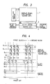
- a matrix circuit 2 is provided for matrix-connection between the internal video signal lines of each block and external video signal lines having the same number of lines as the former lines.
- Sample/hold switching elements constructed of a B-TFT (block dividing TFT) array 3 are interposed on the respective internal video lines between the matrix circuit 2 and the display panel 1. Control signals are supplied to the switching elements of each block to drive the display panel in time division using one horizontal period (1H) as a reversal period.
- FIG. 4 showing a detailed connection diagram of Fig. 3, external video signal lines D1, D2. ..., Dm are divided into m internal video signal lines S1, S2, ..., Sm per one block by the matrix circuit 2. In case of k blocks, the total number of video signal lines is m ⁇ k .
- Each of the internal video signal lines S1, S2, ..., Sm is grounded via a hold capacitor 10.
- Switching elements 11 interposed between the capacitor and the matrix circuit are driven in time division by respective block division gate drivers B1, B2, ..., Bk to output video signals to pixels.
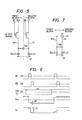
- Fig. 5 illustrates the principle of the charge sharing effect
- Fig. 6 is a timing chart showing the charge sharing effect.
- a central broken line indicates the intersection between blocks, the block at the left of the line being called block 1 and that at the right being called block 2.
- the last signal line Sm of block 1 is driven by the output signal ' from the last source line Dm and the drive voltage B1; for the block division TFT's of block 1.
- the first signal line S1: of block 2 is driven by the output signal from the first source line D1 and the drive voltage B2 for the block division TFT's of block 2, source line capacitance Cm and C1 as seen from source terminal side of the block division TFT's, correspond to the video signal hold capacitor C.
- Interline capacitance Css producing ⁇ V appears between the source lines.
- a gate pulse is applied to line B1
- a video signal on line Dm is transferred to line Sm via the B-TFT to charge the source line capacitor Cm.
- another gate pulse is applied to line B2 to thereby charge the source lines including line S1 of block 2.
- the charging waveforms on lines Sm and S1 at the intersection between the two blocks change as shown in Fig. 6.
- ⁇ V shown by oblique lines is superposed on line Sm and its video signal becomes larger in amplitude than its original, while the video signal on line S1 changes at the start of reversal as shown by oblique lines.
- Such phenomenon results from the charge sharing effect of the source interline capacitance Css between the capacitors Cm and C1.
- the present invention seeks to solve the above problems and provide: a liquid crystal device and method of driving the same wherein high intensity lines of blocks produced by the charge sharing effect during 1H reversal driving are suppressed thereby realizing a high quality of image.
- the present invention provides in a method of driving a liquid crystal device wherein internal video signal lines of a TFT active matrix panel are divided into a plurality of blocks, a matrix circuit is provided for matrix-connection between the internal video signal lines of each block and external video signal lines having the same number of lines as the former lines, sample/hold switching elements are interposed on the respective internal video lines between the matrix circuit and the panel, and control signals are supplied to the switching elements of each block to drive the panel in time division using one horizontal period as a reversal period; a method of driving a liquid crystal device wherein the switching elements of each block are further divided into two half-blocks, a switching signal line is provided for each of the half-blocks, the phase of a control signal applied to the switching elements for each of the half-blocks is shifted between adjacent half-blocks to output video signals onto the internal video signal lines at superposed timings.
- the present invention enables to make a potential difference between signals on Sm and S1 very small.
- the B-TFT array of switching elements of each block is further divided into two half-blocks.
- a switching signal line is provided for each of the half-blocks, the phase of a control signal applied to the switching elements for each of the half-blocks is shifted between adjacent half-blocks to output video signals onto the internal video signal lines at superposed timings.
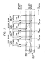
- Fig. 1 is a connection diagram showing the B-TFT's and matrix circuit embodying the present invention.
- a same display panel as a conventional one shown in Fig. 3 is used.
- a TFT active matrix circuit constituting a display portion, B-TFT array and matrix circuit are fabricated on a single substrate.
- the total number of matrix wirings is 240 which are here identified as first half 120 wirings and latter half 120 wirings.
- Video signal lines of one block, i.e., panel source lines are connected to 240 bit B-TFT's.
- the panel source lines and B-TFT's are similarly identified as first half 120 ones and latter half ones.
- a control signal line for turning on and off the B-TFT's of the first 120 bits of block 1 is identified as "B1-first", while a control signal line for turning on and off the B-TFT's of the latter 120 bits of block 1 as “B1-latter”. Similar identification is made up to "B8-latter”.
- the total number of panel source lines is 8 ⁇ 240.
- the number of gate lines (scanning lines) is 480 and the panel corresponds to a TV screen of about 7 inches.
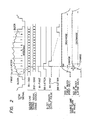
- Fig. 2 is a timing chart showing the operation of the liquid crystal device of Fig. 1 wherein an NTSC television signal is used as a video signal source.
- the television video signal is divided into eight portions which are assigned to blocks 1 to 8 as a video signal source of the display panel, each of the blocks being divided into the first half and the latter half.
- the divided video signal is processed by controlling the output timings of the source line driver as in the following.
- the phase of the on/off control signals on "B1-first” and “B1-latter” and so on is shifted so as to superpose by 90 phase degree between adjacent two half-blocks. Similar timings of the control signals are repeated up to block 8 to write a 1H television signal on 1920 source lines.
- the liquid crystal TN liquid crystal, ferroelectric liquid crystal
- the liquid crystal is ac-driven by grounding the opposing electrode or by reversing every 1H in synchro with the television signal.
- the source line waveforms in the panel shown in Fig. 2 are observed.
- the potential difference V on the source line S121 is very small at the time when a pulse on "B1-first" for the fource line S120 of block 1 turns off. This V corresponds !5 to the V of the above-described approximate formula. Therefore, ⁇ V in the formula becomes considerably small.
- the potential difference ⁇ V at the leading edge of the source line waveform shown in Fig. 2 becomes extremely small.
- One block of the above embodiment may be divided into three or more.
- the resultant potential difference can be reduced to a minimum by driving the finely divided blocks at superposed timings. Further, in case the charge speed with a B-TFT is high, the potential difference can theoretically be made zero. Thus, it is possible to eliminate high intensity lines at the intersection of blocks and provide a liquid crystal device and method of driving the same capable of obtaining a high image quality.
Abstract
Description
- The present invention relates to a liquid crystal device and a method of driving the same, and more particularly to a liquid crystal device and a method of driving the same capable of suppressing high intensity lines produced while driving the device in unit of blocks by using TFT's (thin film transistors) as switching elements.
- As shown in Fig. 3, in a conventional method of driving a liquid crystal panel having a TFT active matrix circuit, internal video signal lines of a
display panel 1 are divided into a plurality of blocks. Amatrix circuit 2 is provided for matrix-connection between the internal video signal lines of each block and external video signal lines having the same number of lines as the former lines. Sample/hold switching elements constructed of a B-TFT (block dividing TFT)array 3 are interposed on the respective internal video lines between thematrix circuit 2 and thedisplay panel 1. Control signals are supplied to the switching elements of each block to drive the display panel in time division using one horizontal period (1H) as a reversal period. - Referring to Fig. 4 showing a detailed connection diagram of Fig. 3, external video signal lines D1, D2. ..., Dm are divided into m internal video signal lines S1, S2, ..., Sm per one block by the
matrix circuit 2. In case of k blocks, the total number of video signal lines is m × k. Each of the internal video signal lines S1, S2, ..., Sm is grounded via ahold capacitor 10.Switching elements 11 interposed between the capacitor and the matrix circuit are driven in time division by respective block division gate drivers B1, B2, ..., Bk to output video signals to pixels. - When a liquid crystal panel constructed as above is driven using one horizontal period (1H) as reversal period, a charge shift phenomenon of a so-called charge sharing effect occurs at the intersection between divided blocks, e.g., between lines Sm and S1 of Fig. 4, due to capacitance between source lines of B-TFT's. As a result, ΔV is superposed on the video signal of line Sm so that a video signal having a larger voltage amplitude than the original video signal is outputted (with
opposing electrode 12 being grounded). - Fig. 5 illustrates the principle of the charge sharing effect, and Fig. 6 is a timing chart showing the charge sharing effect. In Fig. 5, a central broken line indicates the intersection between blocks, the block at the left of the line being called
block 1 and that at the right being calledblock 2. The last signal line Sm ofblock 1 is driven by the output signal ' from the last source line Dm and the drive voltage B1; for the block division TFT's ofblock 1. The first signal line S1: ofblock 2 is driven by the output signal from the first source line D1 and the drive voltage B2 for the block division TFT's ofblock 2, source line capacitance Cm and C1 as seen from source terminal side of the block division TFT's, correspond to the video signal hold capacitor C. Interline capacitance Css producing ΔV appears between the source lines. Referring now to Fig. 6, when a gate pulse is applied to line B1, a video signal on line Dm is transferred to line Sm via the B-TFT to charge the source line capacitor Cm. After charging the source lines ofblock 1 to which the capacitor Cm belongs is completed, another gate pulse is applied to line B2 to thereby charge the source lines including line S1 ofblock 2. In this case, the charging waveforms on lines Sm and S1 at the intersection between the two blocks change as shown in Fig. 6. Particularly, ΔV shown by oblique lines is superposed on line Sm and its video signal becomes larger in amplitude than its original, while the video signal on line S1 changes at the start of reversal as shown by oblique lines. Such phenomenon results from the charge sharing effect of the source interline capacitance Css between the capacitors Cm and C1. The relationship between Δv and V is approximately defined as in the following formula.
ΔV ≒ Css/(C + Css) · V(v)
(C = Cm ≒ C1) - If a liquid crystal display panel as above is driven without any correction, the last lines Sm of the blocks are highly brightened so that it is quite unsuitable for a display device.
- The present invention seeks to solve the above problems and provide: a liquid crystal device and method of driving the same wherein high intensity lines of blocks produced by the charge sharing effect during 1H reversal driving are suppressed thereby realizing a high quality of image.
- In order to solve the above problems, the present invention provides in a method of driving a liquid crystal device wherein internal video signal lines of a TFT active matrix panel are divided into a plurality of blocks, a matrix circuit is provided for matrix-connection between the internal video signal lines of each block and external video signal lines having the same number of lines as the former lines, sample/hold switching elements are interposed on the respective internal video lines between the matrix circuit and the panel, and control signals are supplied to the switching elements of each block to drive the panel in time division using one horizontal period as a reversal period; a method of driving a liquid crystal device wherein the switching elements of each block are further divided into two half-blocks, a switching signal line is provided for each of the half-blocks, the phase of a control signal applied to the switching elements for each of the half-blocks is shifted between adjacent half-blocks to output video signals onto the internal video signal lines at superposed timings.
-
- Fig. 1 is a connection diagram showing the main part of the liquid crystal device according to an embodiment of the present invention;
- Fig. 2 is a timing chart showing the operation of the device of Fig. 1;
- Fig. 3 is a schematic block diagram showing the liquid crystal device according to the prior art;
- Fig. 4 is a timing chart showing the operation of the device of Fig. 3;
- Fig. 5 is an equivalent circuit illustrating the charge sharing effect;
- Fig. 6 is a timing chart showing the operation of the equivalent circuit; and
- Fig. 7 is an equivalent circuit during time-division driving.
- The charge sharing effect occurs during the time from when a pulse is applied to turn on the B-TFT's of one block and to when another pulse is applied to turn on the B-TFT's of the next block. In Fig. 5, during turning-off of the B-TFT at line B1, line Sm keeps a potential charged in the capacitor Cm and maintains open relative to the signal source such as the source line driver of Fig. 3. When a signal is applied during this open state to the B-TFT's of the
next block 2 to turn them, line S1 is enabled to receive the signal from the signal source so that the capacitor C1 is charged. Simultaneously, the signal on line S1 charges the capacitor Css and its charge is transferred to and stored in the capacitor Cm. As a result, the waveform of line Sm changes by ΔV as shown in Fig. 6 Fig. 7 is an equivalent circuit wherein line Sm maintains open and thesignal source 13 is coupled to line S1. - In order to eliminate or decrease ΔV, it can be considered that isolation from the signal source and connection to the signal source should not be conducted simultaneously between the lines of adjacent blocks and that Css and V be made small. Since Css is determined from the panel configuration, the remaining factors to solve the problem of ΔV are switching timings and the value V.
- Paying attention to the switching timings, the present invention enables to make a potential difference between signals on Sm and S1 very small. Particularly, the B-TFT array of switching elements of each block is further divided into two half-blocks. A switching signal line is provided for each of the half-blocks, the phase of a control signal applied to the switching elements for each of the half-blocks is shifted between adjacent half-blocks to output video signals onto the internal video signal lines at superposed timings.
- The embodiment of the present invention will now be described in detail with reference to the accompanying drawings.
- Fig. 1 is a connection diagram showing the B-TFT's and matrix circuit embodying the present invention. In this embodiment, a same display panel as a conventional one shown in Fig. 3 is used. A TFT active matrix circuit constituting a display portion, B-TFT array and matrix circuit are fabricated on a single substrate. In Fig. 1, the total number of matrix wirings is 240 which are here identified as first half 120 wirings and latter half 120 wirings. Video signal lines of one block, i.e., panel source lines are connected to 240 bit B-TFT's. The panel source lines and B-TFT's are similarly identified as first half 120 ones and latter half ones.
- A control signal line for turning on and off the B-TFT's of the first 120 bits of
block 1 is identified as "B1-first", while a control signal line for turning on and off the B-TFT's of the latter 120 bits ofblock 1 as "B1-latter". Similar identification is made up to "B8-latter". Thus, the total number of panel source lines is 8 × 240. The number of gate lines (scanning lines) is 480 and the panel corresponds to a TV screen of about 7 inches. - Fig. 2 is a timing chart showing the operation of the liquid crystal device of Fig. 1 wherein an NTSC television signal is used as a video signal source. The television video signal is divided into eight portions which are assigned to
blocks 1 to 8 as a video signal source of the display panel, each of the blocks being divided into the first half and the latter half. In the present invention, the divided video signal is processed by controlling the output timings of the source line driver as in the following. - When image data of the first 120 bits of
block 1 is inputted, this data is outputted on source lines D1 to D120. Simultaneously therewith, a pulse for turning on the B-TFT's of the first 120 bits is applied to control line "B1-first" to charge the first 120 source Iines ofblock 1. Next, when image data of the latter 120 bits ofblock 1 is prepared, this data is outputted on source lines D121 to D240. Simultaneously therewith, a pulse for turning on the B-TFT's of the latter 120 bits is applied to control line "B1-latter" to charge the latter 120 source lines ofblock 1. The phase of the on/off control signals on "B1-first" and "B1-latter" and so on is shifted so as to superpose by 90 phase degree between adjacent two half-blocks. Similar timings of the control signals are repeated up to block 8 to write a 1H television signal on 1920 source lines. In this case, the liquid crystal (TN liquid crystal, ferroelectric liquid crystal) is ac-driven by grounding the opposing electrode or by reversing every 1H in synchro with the television signal. - In the above liquid crystal drive, the source line waveforms in the panel shown in Fig. 2, particularly the charge/discharge waveforms of the source lines S120 and S121 at the intersection of blocks, are observed. The potential difference V on the source line S121 is very small at the time when a pulse on "B1-first" for the fource line S120 of
block 1 turns off. This V corresponds !5 to the V of the above-described approximate formula. Therefore, ΔV in the formula becomes considerably small. The potential difference ΔV at the leading edge of the source line waveform shown in Fig. 2 becomes extremely small. - One block of the above embodiment may be divided into three or more.
- As seen from the foregoing description of the present invention, even if the charge sharing effect occurs during 1H reversal drive, the resultant potential difference can be reduced to a minimum by driving the finely divided blocks at superposed timings. Further, in case the charge speed with a B-TFT is high, the potential difference can theoretically be made zero. Thus, it is possible to eliminate high intensity lines at the intersection of blocks and provide a liquid crystal device and method of driving the same capable of obtaining a high image quality.
Claims (8)
a display panel wherein internal video signal lines of a TFT active matrix panel are divided into a plurality of blocks, a matrix circuit is provided for matrix-connection between the internal video signal lines of each block and external video signal lines having the same number of lines as the former lines, sample/hold switching elements are interposed on the respective internal video lines between the matrix circuit and the matrix panel, and control signals are supplied to the switching elements of each block to drive the panel in time division using one horizontal period as a reversal period; and output means wherein said switching elements of each block are further divided into two half-blocks, a switching signal line is provided for each of said half-blocks, the phase of a control signal applied to said switching elements for each of said half-blocks is shifted between adjacent half-blocks to output video signals onto said internal video signal lines at superposed timings.
a liquid crystal device wherein internal video signal lines of a TFT active matrix panel are divided into a plurality of blocks, a matrix circuit is provided for matrix-connection between the internal video signal lines of each block and external video signal lines having the same number of lines as the former lines, sample/hold switching elements are interposed on the respective internal video lines between the matrix circuit and the panel, and control signals are supplied to the switching elements of each block to drive the panel in time division using one horizontal period as a reversal period; and output means wherein said switching elements of each block are further divided into half-blocks, a switching signal line is provided for each of said half-blocks, the phase of a control signal applied to said switching elements for each of said half-blocks is shifted between adjacent half-blocks to output video signals onto said internal video signal lines at superposed timings.
Applications Claiming Priority (2)
| Application Number | Priority Date | Filing Date | Title |
|---|---|---|---|
| JP60194803A JPS6255625A (en) | 1985-09-05 | 1985-09-05 | Driving method for liquid crystal device |
| JP194803/85 | 1985-09-05 |
Publications (3)
| Publication Number | Publication Date |
|---|---|
| EP0213630A2 true EP0213630A2 (en) | 1987-03-11 |
| EP0213630A3 EP0213630A3 (en) | 1989-05-10 |
| EP0213630B1 EP0213630B1 (en) | 1993-12-01 |
Family
ID=16330518
Family Applications (1)
| Application Number | Title | Priority Date | Filing Date |
|---|---|---|---|
| EP86112116A Expired - Lifetime EP0213630B1 (en) | 1985-09-05 | 1986-09-02 | Liquid crystal device and method of driving same |
Country Status (4)
| Country | Link |
|---|---|
| US (1) | US4779086A (en) |
| EP (1) | EP0213630B1 (en) |
| JP (1) | JPS6255625A (en) |
| DE (1) | DE3689343T2 (en) |
Cited By (1)
| Publication number | Priority date | Publication date | Assignee | Title |
|---|---|---|---|---|
| EP0546780A1 (en) * | 1991-12-10 | 1993-06-16 | Xerox Corporation | AM TFT LCD universal controller |
Families Citing this family (13)
| Publication number | Priority date | Publication date | Assignee | Title |
|---|---|---|---|---|
| JPS6125184A (en) * | 1984-07-13 | 1986-02-04 | 株式会社 アスキ− | Display controller |
| US4960719A (en) * | 1988-02-04 | 1990-10-02 | Seikosha Co., Ltd. | Method for producing amorphous silicon thin film transistor array substrate |
| JPH01217421A (en) * | 1988-02-26 | 1989-08-31 | Seikosha Co Ltd | Amorphous silicon thin film transistor array substrate and its production |
| JP3126360B2 (en) * | 1989-09-01 | 2001-01-22 | キヤノン株式会社 | Display system and display control method thereof |
| US6124842A (en) * | 1989-10-06 | 2000-09-26 | Canon Kabushiki Kaisha | Display apparatus |
| US5063378A (en) * | 1989-12-22 | 1991-11-05 | David Sarnoff Research Center, Inc. | Scanned liquid crystal display with select scanner redundancy |
| JP3364114B2 (en) * | 1997-06-27 | 2003-01-08 | シャープ株式会社 | Active matrix type image display device and driving method thereof |
| JP4147872B2 (en) * | 2002-09-09 | 2008-09-10 | 日本電気株式会社 | Liquid crystal display device, driving method thereof, and liquid crystal projector device |
| US7050027B1 (en) | 2004-01-16 | 2006-05-23 | Maxim Integrated Products, Inc. | Single wire interface for LCD calibrator |
| US20050206597A1 (en) * | 2004-02-10 | 2005-09-22 | Seiko Epson Corporation | Electro-optical device, method for driving electro-optical device, driving circuit, and electronic apparatus |
| JP2010122355A (en) | 2008-11-18 | 2010-06-03 | Canon Inc | Display apparatus and camera |
| JP2010164666A (en) | 2009-01-14 | 2010-07-29 | Hitachi Displays Ltd | Driver circuit, liquid crystal display device, and output signal control method |
| JP2012018320A (en) | 2010-07-08 | 2012-01-26 | Hitachi Displays Ltd | Display device |
Citations (1)
| Publication number | Priority date | Publication date | Assignee | Title |
|---|---|---|---|---|
| JPS59221183A (en) * | 1983-05-31 | 1984-12-12 | Seiko Epson Corp | Driving system of liquid crystal display type picture receiver |
Family Cites Families (3)
| Publication number | Priority date | Publication date | Assignee | Title |
|---|---|---|---|---|
| JPS56156884A (en) * | 1980-05-09 | 1981-12-03 | Hitachi Ltd | Method of driving gas discharge display element |
| JPS59123884A (en) * | 1982-12-29 | 1984-07-17 | シャープ株式会社 | Driving of liquid crystal display |
| JPS61117599A (en) * | 1984-11-13 | 1986-06-04 | キヤノン株式会社 | Switching pulse for video display unit |
-
1985
- 1985-09-05 JP JP60194803A patent/JPS6255625A/en active Granted
-
1986
- 1986-08-29 US US06/901,826 patent/US4779086A/en not_active Expired - Lifetime
- 1986-09-02 EP EP86112116A patent/EP0213630B1/en not_active Expired - Lifetime
- 1986-09-02 DE DE86112116T patent/DE3689343T2/en not_active Expired - Lifetime
Patent Citations (1)
| Publication number | Priority date | Publication date | Assignee | Title |
|---|---|---|---|---|
| JPS59221183A (en) * | 1983-05-31 | 1984-12-12 | Seiko Epson Corp | Driving system of liquid crystal display type picture receiver |
Cited By (1)
| Publication number | Priority date | Publication date | Assignee | Title |
|---|---|---|---|---|
| EP0546780A1 (en) * | 1991-12-10 | 1993-06-16 | Xerox Corporation | AM TFT LCD universal controller |
Also Published As
| Publication number | Publication date |
|---|---|
| DE3689343D1 (en) | 1994-01-13 |
| EP0213630A3 (en) | 1989-05-10 |
| DE3689343T2 (en) | 1994-05-11 |
| US4779086A (en) | 1988-10-18 |
| JPS6255625A (en) | 1987-03-11 |
| EP0213630B1 (en) | 1993-12-01 |
| JPH0448365B2 (en) | 1992-08-06 |
Similar Documents
| Publication | Publication Date | Title |
|---|---|---|
| JP2783412B2 (en) | Matrix display device | |
| JP4154611B2 (en) | Shift register and liquid crystal display device | |
| US4651148A (en) | Liquid crystal display driving with switching transistors | |
| EP0863498B1 (en) | Data signal line structure in an active matrix liquid crystal display | |
| US6756953B1 (en) | Liquid crystal display device implementing gray scale based on digital data as well as portable telephone and portable digital assistance device provided with the same | |
| EP1052615B1 (en) | Method of driving a flat panel display device | |
| US4779086A (en) | Liquid crystal device and method of driving same | |
| EP0216188A2 (en) | Matrix display panel | |
| JPS5875194A (en) | Matrix display and driving method | |
| US5777591A (en) | Matrix display apparatus employing dual switching means and data signal line driving means | |
| EP0487045B1 (en) | Liquid crystal apparatus and method of driving the same | |
| US6498595B1 (en) | Active matrix liquid crystal display devices | |
| JPH07181927A (en) | Image display device | |
| JPH1124632A (en) | Active matrix type image display device and its driving method | |
| US6304242B1 (en) | Method and apparatus for displaying image | |
| JPH07199154A (en) | Liquid crystal display device | |
| JPH06337657A (en) | Liquid crystal display device | |
| US5900853A (en) | Signal line driving circuit | |
| JP2552070B2 (en) | Active matrix display device and driving method thereof | |
| JPH05260418A (en) | Liquid crystal display device | |
| JP2001272657A (en) | Liquid crystal element | |
| JPH10149141A (en) | Liquid crystal display device | |
| JP3192547B2 (en) | Driving method of liquid crystal display device | |
| JPH02123326A (en) | Liquid crystal display device and its driving method | |
| JP3400082B2 (en) | Liquid crystal display |
Legal Events
| Date | Code | Title | Description |
|---|---|---|---|
| PUAI | Public reference made under article 153(3) epc to a published international application that has entered the european phase |
Free format text: ORIGINAL CODE: 0009012 |
|
| AK | Designated contracting states |
Kind code of ref document: A2 Designated state(s): CH DE FR GB LI NL |
|
| PUAL | Search report despatched |
Free format text: ORIGINAL CODE: 0009013 |
|
| AK | Designated contracting states |
Kind code of ref document: A3 Designated state(s): CH DE FR GB LI NL |
|
| 17P | Request for examination filed |
Effective date: 19890922 |
|
| 17Q | First examination report despatched |
Effective date: 19910610 |
|
| GRAA | (expected) grant |
Free format text: ORIGINAL CODE: 0009210 |
|
| AK | Designated contracting states |
Kind code of ref document: B1 Designated state(s): CH DE FR GB LI NL |
|
| REF | Corresponds to: |
Ref document number: 3689343 Country of ref document: DE Date of ref document: 19940113 |
|
| ET | Fr: translation filed | ||
| PLBE | No opposition filed within time limit |
Free format text: ORIGINAL CODE: 0009261 |
|
| STAA | Information on the status of an ep patent application or granted ep patent |
Free format text: STATUS: NO OPPOSITION FILED WITHIN TIME LIMIT |
|
| 26N | No opposition filed | ||
| REG | Reference to a national code |
Ref country code: GB Ref legal event code: IF02 |
|
| PGFP | Annual fee paid to national office [announced via postgrant information from national office to epo] |
Ref country code: FR Payment date: 20050823 Year of fee payment: 20 |
|
| PGFP | Annual fee paid to national office [announced via postgrant information from national office to epo] |
Ref country code: DE Payment date: 20050825 Year of fee payment: 20 |
|
| PGFP | Annual fee paid to national office [announced via postgrant information from national office to epo] |
Ref country code: GB Payment date: 20050831 Year of fee payment: 20 |
|
| PGFP | Annual fee paid to national office [announced via postgrant information from national office to epo] |
Ref country code: CH Payment date: 20050914 Year of fee payment: 20 |
|
| PGFP | Annual fee paid to national office [announced via postgrant information from national office to epo] |
Ref country code: NL Payment date: 20050915 Year of fee payment: 20 |
|
| REG | Reference to a national code |
Ref country code: GB Ref legal event code: PE20 |
|
| PG25 | Lapsed in a contracting state [announced via postgrant information from national office to epo] |
Ref country code: GB Free format text: LAPSE BECAUSE OF EXPIRATION OF PROTECTION Effective date: 20060901 |
|
| PG25 | Lapsed in a contracting state [announced via postgrant information from national office to epo] |
Ref country code: NL Free format text: LAPSE BECAUSE OF EXPIRATION OF PROTECTION Effective date: 20060902 |
|
| REG | Reference to a national code |
Ref country code: CH Ref legal event code: PL |
|
| NLV7 | Nl: ceased due to reaching the maximum lifetime of a patent |
Effective date: 20060902 |