EP0211960A1 - Matrix-vermittlungsanordnung - Google Patents
Matrix-vermittlungsanordnung Download PDFInfo
- Publication number
- EP0211960A1 EP0211960A1 EP86901487A EP86901487A EP0211960A1 EP 0211960 A1 EP0211960 A1 EP 0211960A1 EP 86901487 A EP86901487 A EP 86901487A EP 86901487 A EP86901487 A EP 86901487A EP 0211960 A1 EP0211960 A1 EP 0211960A1
- Authority
- EP
- European Patent Office
- Prior art keywords
- memory
- control
- interface
- array
- signal
- Prior art date
- Legal status (The legal status is an assumption and is not a legal conclusion. Google has not performed a legal analysis and makes no representation as to the accuracy of the status listed.)
- Withdrawn
Links
Images



Classifications
-
- H—ELECTRICITY
- H03—ELECTRONIC CIRCUITRY
- H03K—PULSE TECHNIQUE
- H03K19/00—Logic circuits, i.e. having at least two inputs acting on one output; Inverting circuits
- H03K19/02—Logic circuits, i.e. having at least two inputs acting on one output; Inverting circuits using specified components
- H03K19/173—Logic circuits, i.e. having at least two inputs acting on one output; Inverting circuits using specified components using elementary logic circuits as components
- H03K19/177—Logic circuits, i.e. having at least two inputs acting on one output; Inverting circuits using specified components using elementary logic circuits as components arranged in matrix form
- H03K19/17704—Logic circuits, i.e. having at least two inputs acting on one output; Inverting circuits using specified components using elementary logic circuits as components arranged in matrix form the logic functions being realised by the interconnection of rows and columns
- H03K19/17708—Logic circuits, i.e. having at least two inputs acting on one output; Inverting circuits using specified components using elementary logic circuits as components arranged in matrix form the logic functions being realised by the interconnection of rows and columns using an AND matrix followed by an OR matrix, i.e. programmable logic arrays
- H03K19/17712—Logic circuits, i.e. having at least two inputs acting on one output; Inverting circuits using specified components using elementary logic circuits as components arranged in matrix form the logic functions being realised by the interconnection of rows and columns using an AND matrix followed by an OR matrix, i.e. programmable logic arrays one of the matrices at least being reprogrammable
-
- H—ELECTRICITY
- H03—ELECTRONIC CIRCUITRY
- H03K—PULSE TECHNIQUE
- H03K17/00—Electronic switching or gating, i.e. not by contact-making and –breaking
- H03K17/002—Switching arrangements with several input- or output terminals
-
- H—ELECTRICITY
- H03—ELECTRONIC CIRCUITRY
- H03K—PULSE TECHNIQUE
- H03K5/00—Manipulating of pulses not covered by one of the other main groups of this subclass
- H03K5/13—Arrangements having a single output and transforming input signals into pulses delivered at desired time intervals
- H03K5/131—Digitally controlled
Definitions
- the present invention relates to a matrix switch circuit adapted for use as a delay map former that is employed in an ultrasonograph of the phased array sector scan type.
- An ultrasonograph of the phased array sector scan type comprises a phased array of ultrasonic transducers that are brought into contact with an object to be examined. Ultrasonic beams are emitted into the object from the transducers at successively differing angles to make a sector scan. The resultant echo signals are processed to obtain an ultrasonogram of the object.
- the echo signals received by the transducers are put in phase via a delay map former having delay elements whose delay times are controlled according to the respective echo signals.
- This delay map former consists of a combination of a matrix switch and a tapped delay circuit.
- Fig. 10 is a block diagram of the conventional matrix switch that is used to build a delay map former.
- the switch has an address decoder 1 for decoding the incoming address signal, a control memory 2 that receives data regarding addresses from the decoder 1, and an analog switch array 3 which is controlled by the signal from the memory 2.
- the array 3 consists of a matrix of 8 x 8 switches.
- the decorder 1 receives ADDRESS ENABLE signal AE and address signals A 0 -A 2 .
- the memory 2 can consist, for example, of a memory whose contents can be rewritten, such as a random-access memory. Data items DO-D 7 are written to the memory 2 at addresses specified by the address decoder 1, according to the ADDRESS ENABLE signal.
- the analog switch array 3 consists of a matrix of switches, 64 switches in this case, disposed at the intersections of vertical lines (junctors) and horizontal lines. These switches are closed or opened, according to their respective output signals from the memory 2. Indicated by V DD , V EE' and V SS are supply voltages.
- Echo signals received by a plurality of ultrasonic transducers are supplied either to the vertical lines J O -J 7 or to the horizontal lines L 0 -L 7 , respectively. Those lines which are not fed with the echo signals are connected with the taps of a tapped delay circuit (not shown). Data concerning a desired delay map is written to the control memory 2 to selectively close the switches of the array 3. Thus, the echo signals received by the transducers are delayed by periods matched to a desired directivity of reception.
- the vertical and horizontal lines are selectively enabled, according to the contents of the control memory 2. Therefore, even when the contents of the memory 2 are being altered, the switches of the array are selectively closed, according to the present contents of the memory. However, the contents of the memory 2 make no meaning until the contents of the memory are fully rewritten. For this reason, it is necessary to inhibit the vertical or horizontal lines while the contents of the memory 2 are being rewritten.
- the data stored in the memory 2 is rewritten each time one echo signal is received as shown in Fig. 11. It is now assumed that an echo signal is received from instant t 1 to instant t 2 , using a delay map. Thereafter, neither the transmission of ultrasound nor the reception of echo signals is performed during the interval between instant t 2 and instant t 3 . During this interval, the data stored in the memory 2 is rewritten, according to the directivity of the next echo reception. Where a hundred 8 x 8 matrix switches are used in combination to make use of 6400 switches in total, about 40 ⁇ s is taken to rewrite the contents of the memory 2. This has made it impossible to send and receive ultrasonic waves at a high rate.
- an interface is provided between a control memory and an array of analog switches so that the contents of the memory are momentarily read out and held in the interface.
- the held signal is used to control the closure or opening of each of the switches of the array.
- a matrix switch circuit embodying the concept of the invention is similar to the conventional circuit shown in Fig. 10 except that a first control memory 2a, a second control memory 2b, and an interface 4 are provided.
- the first memory 2a receives ADDRESS LINE SELECT signals S 0 , S 1 , ..., S 7 from address decoder 1
- the second memory 2b receives ADDRESS LINE SELECT signals S 8 , S 9 , ..., S 15 from the decoder 1.
- the data read from the memories 2a and 2b is fed to analog switch array 3 via the interface 4.
- the decoder 1 receives ADDRESS ENABLE signal AE and address signals A 0 -A 3 and deliver ADDRESS LINE SELECT signals S 0 -S 15 .
- Data signals Do-D 7 and MASTER RESET signal MR are applied to both memories 2a and 2b. Each of the memories 2a and 2b delivers 64 data items to control the switches of the array.
- the interface 4 receives the output signal from the memories 2a, 2b, INTERFACE ENABLE signal IE, and most significant address signal A3.
- the interface 4 delivers 64 signals to the array 3 to control the matrix of the switches.
- the decoder l, the memories 2a, 2b, and the interface 4 handle digital signals.
- the array 3 interconnects some of input lines L 0 -L 7 and output lines J O -J 7 via those switches which are closed in response to the control signals from the interface 4. Analog signals are allowed to pass through the interface via the interconnected lines.
- the apparatus constructed as described above operates in the manner described below.
- ADDRESS ENABLE signal AE goes high
- the address signals A 0 -A 3 applied to the address decoder 1 are decoded, and one of LINE SELECT signals S 0 -S 15 goes high.
- the most significant bit A3 of the address signals acts as a BANK SELECT signal that determines to which of the first and second control memories is data written.
- the selected memory 2a or 2b writes data items D 0 -D 7 to those address lines whose corresponding LINE SELECT signals go high, and stores them.
- the LINE SELECT signals are successively caused to go high in order to sequentially write data to the address lines. In this example, after data has been written to both memories 2a and 2b, it follows that 128 data items in total are stored in them.
- the memories 2a and 2b can be reset by supplying MASTER RESET signal MR to them as the need arises.
- the interface 4 selects the 64 matrix switch control signals from the memory 2a or 2b that is not selected by the aforementioned BANK SELECT signal.
- INTERFACE ENABLE signal IE is at high level, the interface 4 accepts the selected signals. Then, the signals are held in the holding means (not shown) of the interface and supplied to the array 3 to control the switches. In this way, each of 8 x 8 switches of the array 3 is closed or opened, depending on the control signals from the interface 4. As a result, the vertical and horizontal lines are selectively enabled, according to the data previously written to the control memories.
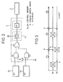
- Fig. 2 is a block diagram of one example of the interface 4 shown in Fig. 1.
- the illustrated circuit corresponds to one of the data items delivered from one control memory.
- 64 similar circuits are incorporated in the interface 4.
- the circuit shown in Fig. 2 comprises an AND gate Gl, another AND gate G2, an OR gate G3 that ORs the output signals from the gates Gl and G2, a switch circuit LC that interrupts the output from the OR gate G3 according to INTERFACE ENABLE signal IE, and a flip-flop FF for storing the signal passed through the switch circuit LC.
- the control signal from the first control memory 2a is applied to one input terminal of the AND gate Gl, whose other inverted terminal receives the most significant address signal A3.
- the control signal from the second control memory 2b is applied to one input terminal of the AND gate G2, the other non-inverted terminal of which receives the most significant address signal A3.
- the AND gate Gl or G2 selects either the control signal from the first memory 2a or the control signal from the second memory 2b, depending on the most significant address signal A3.
- the selected control signal is stored in the flip-flop FF by INTERFACE ENABLE signal IE, and is also applied to the analog switch array 3. Therefore, each of the switches of the array 3 is closed or opened according to the data stored in the flip-flop FF. This condition is maintained even after INTERFACE ENABLE signal IE is inverted, isolating the switch circuit LC. At this time, therefore, the contents of the memories 2a and 2b can be changed without affecting the closure or opening of each switch of the array 3.
- a capacitor can be used as the means for holding the matrix switch control signal, instead of the flip-flop FF. In this case, the capacitor may make use of the stray capacitance of the control signal lines for the switches.
- the novel matrix switch circuit can be utilized as a delay map former for an ultrasonograph in the manner described below.
- the contents of the first and second control memories 2a and 2b can be changed at any desired instant simultaneously with reception of echo signals. More specifically, when echo signals are being received in mode 1 in response to the control signal held in the holding means of the interface 4, the contents of the control memory 2a are changed for the next mode 2.
- the operation in mode 2 is started at instant t 2 . At this instant, the contents of the memory 2a are transferred to the holding means of the interface 4.
- the closure or opening of each switch of the array is varied for the mode 2.
- a control signal for mode 3 is written to the memory 2b during the interval between the instant t 1 at which the writing of data to the memory 2a is completed and the instant t 4 at which the reception of echo signals in mode 3 is initiated.
- the written data is transferred to the holding means of the interface 4 at the instant t 4 .
- the memory 2a whose contents were transferred to the holding means at instant t 2 is capable of starting to accept data for mode 4 at the instant t 3 .
- Fig. 4 is a timing chart for illustrating the operation of a sector scan type ultrasonograph with which the novel matrix switch circuit is used.
- the ultrasonograph utilizes Doppler mode.
- a control signal for B mode and a control signal for D (Doppler) mode are alternately mapped onto the memories 2a and 2b.
- D mode a control signal for D
- the delay map used in B mode differs among every echo reception, but the delay map used in D mode remains the same for every echo reception unless the sample position is altered.
- the delay map for B mode can be varied during the period of reception of echo in D mode, if this period does not lie within range gate period RG as shown in Fig. 5.
- a real-time dynamic focusing can be performed for a sector scan. Specifically, when echo signals are being received in B mode, data items which cause the received waves to produce different focal lengths F1, F 2 , F 3 , etc. are successively written-to one control memory 2a. Then, they are transferred to the holding means of the interface 4. Where the reception of a single echo signal persists for 200 us and 40 ⁇ s is taken to rewrite the delay map, dynamic focusing of five stages can be achieved.
- Figs. 7 and 8 are block diagrams of other examples of the invention.
- three control memories 2a, 2b, 2c are provided.
- the interface 4 selects one out of the control signals from the memories 2a-2c, in response to the most significant two bits A3 and A4 of the address signal.
- Fig. 8 uses a single control memory. While the array 3 of the analog switches is being controlled according to the contents of the holding means of the interface 4, the contents of the control memory 2 are changed.
- Fig. 9 is a timing chart for illustrating the operation for receiving echo signals in B and D modes in accordance with this example.
- the novel matrix switch circuit permits the contents of at least one control memory to be changed while maintaining the condition of the vertical and horizontal lines, i.e., allowing signals to pass through the switches.
Landscapes
- Physics & Mathematics (AREA)
- Mathematical Physics (AREA)
- Nonlinear Science (AREA)
- Engineering & Computer Science (AREA)
- Computer Hardware Design (AREA)
- Computing Systems (AREA)
- General Engineering & Computer Science (AREA)
- Ultra Sonic Daignosis Equipment (AREA)
- Investigating Or Analyzing Materials By The Use Of Ultrasonic Waves (AREA)
- Electronic Switches (AREA)
Applications Claiming Priority (2)
| Application Number | Priority Date | Filing Date | Title |
|---|---|---|---|
| JP60027769A JPS61187846A (ja) | 1985-02-15 | 1985-02-15 | マトリツクススイツチ回路 |
| JP27769/85 | 1985-02-15 |
Publications (2)
| Publication Number | Publication Date |
|---|---|
| EP0211960A1 true EP0211960A1 (de) | 1987-03-04 |
| EP0211960A4 EP0211960A4 (de) | 1988-09-07 |
Family
ID=12230188
Family Applications (1)
| Application Number | Title | Priority Date | Filing Date |
|---|---|---|---|
| EP19860901487 Withdrawn EP0211960A4 (de) | 1985-02-15 | 1986-02-14 | Matrix-vermittlungsanordnung. |
Country Status (4)
| Country | Link |
|---|---|
| US (1) | US4803486A (de) |
| EP (1) | EP0211960A4 (de) |
| JP (1) | JPS61187846A (de) |
| WO (1) | WO1986005049A1 (de) |
Cited By (2)
| Publication number | Priority date | Publication date | Assignee | Title |
|---|---|---|---|---|
| EP0383952A4 (en) * | 1988-08-31 | 1991-07-03 | Fujitsu Limited | Constitution for expanding logic scale of a programmable logic array |
| FR2711016A1 (fr) * | 1993-10-05 | 1995-04-14 | Thomson Csf | Système de commande d'un arrangement d'éléments transducteurs-électromagnétiques ou électroacoustiques. |
Families Citing this family (4)
| Publication number | Priority date | Publication date | Assignee | Title |
|---|---|---|---|---|
| US5276439A (en) * | 1988-05-23 | 1994-01-04 | Kabushiki Kaisha Toshiba | Digital signal exchange equipment |
| JPH0732843U (ja) * | 1991-12-18 | 1995-06-16 | テクノエクセル株式会社 | 圧力スイッチ装置 |
| JPH0611527U (ja) * | 1992-04-06 | 1994-02-15 | 政▲いち▼ 大畑 | 歯ブラシ |
| US6961303B1 (en) * | 2000-09-21 | 2005-11-01 | Serconet Ltd. | Telephone communication system and method over local area network wiring |
Family Cites Families (9)
| Publication number | Priority date | Publication date | Assignee | Title |
|---|---|---|---|---|
| US4196582A (en) * | 1975-01-06 | 1980-04-08 | Ebauches S.A. | Control device for an electronic watch |
| JPS5926917B2 (ja) * | 1976-03-09 | 1984-07-02 | セイコーエプソン株式会社 | 電子時計 |
| US4065916A (en) * | 1977-01-17 | 1978-01-03 | Texas Instruments Incorporated | Electronic timepiece |
| JPS5435645A (en) * | 1977-08-25 | 1979-03-15 | Hitachi Denshi Ltd | Input/output control system for real-time data |
| JPS54109342A (en) * | 1978-02-15 | 1979-08-27 | Nec Corp | Data processor |
| JPS5677891A (en) * | 1979-11-29 | 1981-06-26 | Tokyo Shibaura Electric Co | Displayyunit drive circuit |
| US4281550A (en) * | 1979-12-17 | 1981-08-04 | North American Philips Corporation | Curved array of sequenced ultrasound transducers |
| DE3120163A1 (de) * | 1981-05-21 | 1982-12-09 | Deutsche Itt Industries Gmbh, 7800 Freiburg | Cmos-auswahlschaltung |
| US4535360A (en) * | 1983-09-27 | 1985-08-13 | At&T Bell Laboratories | Low power wideband switching array element |
-
1985
- 1985-02-15 JP JP60027769A patent/JPS61187846A/ja active Granted
-
1986
- 1986-02-14 EP EP19860901487 patent/EP0211960A4/de not_active Withdrawn
- 1986-02-14 WO PCT/JP1986/000066 patent/WO1986005049A1/ja not_active Ceased
-
1988
- 1988-02-22 US US07/159,487 patent/US4803486A/en not_active Expired - Fee Related
Cited By (3)
| Publication number | Priority date | Publication date | Assignee | Title |
|---|---|---|---|---|
| EP0383952A4 (en) * | 1988-08-31 | 1991-07-03 | Fujitsu Limited | Constitution for expanding logic scale of a programmable logic array |
| US5132570A (en) * | 1988-08-31 | 1992-07-21 | Fujitsu Limited | Extended logical scale structure of a programmable logic array |
| FR2711016A1 (fr) * | 1993-10-05 | 1995-04-14 | Thomson Csf | Système de commande d'un arrangement d'éléments transducteurs-électromagnétiques ou électroacoustiques. |
Also Published As
| Publication number | Publication date |
|---|---|
| WO1986005049A1 (fr) | 1986-08-28 |
| US4803486A (en) | 1989-02-07 |
| JPS61187846A (ja) | 1986-08-21 |
| JPH026531B2 (de) | 1990-02-09 |
| EP0211960A4 (de) | 1988-09-07 |
Similar Documents
| Publication | Publication Date | Title |
|---|---|---|
| US5959930A (en) | Multi-bank synchronous semiconductor memory device | |
| US4882710A (en) | FIFO memory including dynamic memory elements | |
| US4586167A (en) | Semiconductor memory device | |
| JP3092558B2 (ja) | 半導体集積回路装置 | |
| EP0166974A2 (de) | Dynamischer Direktzugriffspeicher | |
| JPH1186534A (ja) | 半導体記憶装置 | |
| US4858190A (en) | Dual port semiconductor memory having random and serial access modes | |
| KR100516301B1 (ko) | 플래시 메모리의 뱅크 분할 장치 | |
| JPH1186532A (ja) | 半導体記憶装置 | |
| KR970017659A (ko) | 반도체 메모리 장치와 그 리이드 및 라이트 방법 | |
| JP3161383B2 (ja) | 半導体記憶装置 | |
| KR100238741B1 (ko) | 판독 전용 메모리 | |
| EP0123411B1 (de) | Parallelverarbeitung gleichzeitiger Ultraschallvektoren | |
| US4475181A (en) | Semiconductor memory | |
| US5088062A (en) | Memory device having common data lines for reading and writing | |
| US4879685A (en) | Semiconductor memory device with internal array transfer capability | |
| US5255220A (en) | Dual port video memory system having pulse triggered dual column addressing | |
| JP3092556B2 (ja) | 半導体記憶装置 | |
| JP2582587B2 (ja) | 半導体記憶装置 | |
| US4803486A (en) | Matrix switch circuit | |
| JPH1040685A (ja) | 同期型記憶装置および同期型記憶装置におけるデータ読み出し方法 | |
| US4891795A (en) | Dual-port memory having pipelined serial output | |
| US4766570A (en) | Semiconductor memory device | |
| JPH1186533A (ja) | 半導体記憶装置 | |
| IE53486B1 (en) | Memory |
Legal Events
| Date | Code | Title | Description |
|---|---|---|---|
| PUAI | Public reference made under article 153(3) epc to a published international application that has entered the european phase |
Free format text: ORIGINAL CODE: 0009012 |
|
| AK | Designated contracting states |
Kind code of ref document: A1 Designated state(s): DE GB |
|
| 17P | Request for examination filed |
Effective date: 19870227 |
|
| DET | De: translation of patent claims | ||
| A4 | Supplementary search report drawn up and despatched |
Effective date: 19880907 |
|
| 17Q | First examination report despatched |
Effective date: 19900511 |
|
| STAA | Information on the status of an ep patent application or granted ep patent |
Free format text: STATUS: THE APPLICATION IS DEEMED TO BE WITHDRAWN |
|
| 18D | Application deemed to be withdrawn |
Effective date: 19900922 |
|
| RIN1 | Information on inventor provided before grant (corrected) |
Inventor name: TAMEZUMI, YOSHIROYOKOGAWA MEDICAL SYSTEMS, LTD. Inventor name: SANO, SHINICHIYOKOGAWA MEDICAL SYSTEMS, LTD. Inventor name: HIGASHIIZUMI, TAKAOYOKOGAWA MEDICAL SYSTEMS, LTD Inventor name: KAKIZAWA, TSUYOSHIYOKOGAWA MEDICAL SYSTEMS, LTD. Inventor name: TAKEUCHI, YASUHITOYOKOGAWA MEDICAL SYSTEMS, LTD. |