EP0210064A2 - Festwertspeicher mit veränderlicher Seite - Google Patents
Festwertspeicher mit veränderlicher Seite Download PDFInfo
- Publication number
- EP0210064A2 EP0210064A2 EP86305575A EP86305575A EP0210064A2 EP 0210064 A2 EP0210064 A2 EP 0210064A2 EP 86305575 A EP86305575 A EP 86305575A EP 86305575 A EP86305575 A EP 86305575A EP 0210064 A2 EP0210064 A2 EP 0210064A2
- Authority
- EP
- European Patent Office
- Prior art keywords
- address
- memory
- address signal
- inputs
- data
- Prior art date
- Legal status (The legal status is an assumption and is not a legal conclusion. Google has not performed a legal analysis and makes no representation as to the accuracy of the status listed.)
- Granted
Links
Images

Classifications
-
- G—PHYSICS
- G11—INFORMATION STORAGE
- G11C—STATIC STORES
- G11C17/00—Read-only memories programmable only once; Semi-permanent stores, e.g. manually-replaceable information cards
-
- G—PHYSICS
- G11—INFORMATION STORAGE
- G11C—STATIC STORES
- G11C8/00—Arrangements for selecting an address in a digital store
- G11C8/12—Group selection circuits, e.g. for memory block selection, chip selection, array selection
-
- G—PHYSICS
- G11—INFORMATION STORAGE
- G11C—STATIC STORES
- G11C16/00—Erasable programmable read-only memories
- G11C16/02—Erasable programmable read-only memories electrically programmable
- G11C16/06—Auxiliary circuits, e.g. for writing into memory
- G11C16/08—Address circuits; Decoders; Word-line control circuits
-
- G—PHYSICS
- G11—INFORMATION STORAGE
- G11C—STATIC STORES
- G11C17/00—Read-only memories programmable only once; Semi-permanent stores, e.g. manually-replaceable information cards
- G11C17/08—Read-only memories programmable only once; Semi-permanent stores, e.g. manually-replaceable information cards using semiconductor devices, e.g. bipolar elements
- G11C17/10—Read-only memories programmable only once; Semi-permanent stores, e.g. manually-replaceable information cards using semiconductor devices, e.g. bipolar elements in which contents are determined during manufacturing by a predetermined arrangement of coupling elements, e.g. mask-programmable ROM
- G11C17/12—Read-only memories programmable only once; Semi-permanent stores, e.g. manually-replaceable information cards using semiconductor devices, e.g. bipolar elements in which contents are determined during manufacturing by a predetermined arrangement of coupling elements, e.g. mask-programmable ROM using field-effect devices
Definitions
- the present invention relates to read only memories (ROM's) and, more particularly, to a read only memory which has a mask programmable page configuration.
- a read only memory is a data storage device which consists of a matrix array of data storage units, such as switches or transistors, which can be individually accessed and read to determine their state ("on” or “off", operable or inoperable).
- Various peripheral circuits are required in order to access and read the storage devices. These circuits include address signal input circuits, address signal decoding circuits, and data transfer circuits.
- Address signals are applied in parallel to the address inputs of an input buffer. If, for example, the address input signal has 17 bits, the input buffer will have 17 address inputs, each connected to receive a different bit of the address signal.
- the address circuitry includes a row address decoder and a column address decoder, both of which receive parallel inputs from the input buffer circuit. In accordance with these inputs, the decoder circuits select a particular storage unit,from the matrix.
- the selected storage unit is read to determine its state which is reflected by either a high or low voltage on an output line.
- Parallel output lines, one for each column, are connected to an output buffer circuit which, in turn, applies a parallel output signal to a data bus.
- the data is programmed into the memory during the fabrication process. Since different data need be programmed into the memories for different applications, it is advisable that the fabrication process be the same for all of the memories of a given type, except for the step during which the information is programmed.
- Read only memories are formed on semiconductor chips through the process of layering the chip surface and then etching selected portions of the layers. The portions to be etched are selected by masking the surface through the use of well known processes.
- the storage unit matrix is programmed through the use of masks and, thus, different masks are utilized to program different information. Information is stored in the memory by physically creating operable or inoperable devices at intersections of the matrix. Once programmed, it cannot be changed, unlike electronically programmable memories which can be erased, either in bulk such as through the use of ultraviolet light or by erasing each unit individually, and reprogrammed.
- Mass production of read only memories with different programming is only possible because the structure of the memory matrix and peripheral circuitry is the same for all memories of a given type, regardless of the information to be programmed therein. Otherwise, a different structure would have to be developed for each program, making production costs prohibitive.
- the configuration of the matrix array and the structure of the peripheral circuitry are designed to be compatible.
- a matrix array of a given size requires a given number of address inputs which must be decoded in a particular manner. If the size or shape (numbers of rows and columns) of the memory matrix is altered, the address circuitry and input circuitry must be correspondingly altered.
- the number of address inputs can be reduced, without loss of capacity, if the memory array is organized into sub-arrays and addressed accordingly. For example, a 4K array of storage units may require ten address inputs--five for the row decoder and five for the column decoder. A 16K array would normally require twice as many address inputs, totalling 20--ten for the row decoder and ten for the column decoder. However, if the 16K array is considered to be four separate 4K sub-arrays, each individually addressable, only a two digit code and, thus, two address inputs, are required to select the proper sub-array.
- Such sub-arrays can be referred to as blocks or banks of storage units, but are most often called “pages" throughout the industry.
- the process of organizing a matrix array into pages is called “pagination”. Random access memories with various page configurations are known. However, because the particular page configuration selected is dependent upon the number of address inputs which are available, and vice versa, different memory designs and peripheral circuit configurations are required for different page configurations.
- Increased memory capacity means that additional memory may be obtained in the same size chip.
- modern 8K read only memory chips can replace older 4K read only memory chips.
- a different ROM design including a paginated storage array, is required if the higher capacity chip is to be substituted for the previously used memory.
- the present invention overcomes this problem through the utilization of a single basic read only memory circuit which is mask programmable to provide a selected one of a variety of different page configurations and, thus, accommodate different numbers of address inputs. This is a great savings in cost because the same basic circuit design can be used for a large variety of applications, simply by utilizing the appropriate pagination masking.
- Each storage array configuration requires a given number of address inputs. If all of these inputs can be supplied by the regular row and column address inputs from the system, no pagination is required. However, if less than the required number of inputs are available from the system through the regular address lines, pagination is required as is a page address signal. The number of required bits in the page address signal is related to the page configuration. Since the page address signal is not available on the regular address inputs, some other way of routing the page address signal to and within the ROM is required.
- the page address signal originates at the microprocessor of the system and is applied to the data bus. During the presence of a control signal, the page address signal bits are routed from the data bus to the decoder circuitry.
- the page address signal bits must be preserved in the read only memory for a time equal to the access time to read the desired number of locations on the designated page and, thereafter, erased.
- Conventional read only memories have no facility for the temporary storage of address signals.
- the present invention utilizes a mask programmable decoder in order to define the page configuration
- a mask programmable input buffer circuit is utilized to block unused row and column address signal paths.
- the page address signal is generated by the system and is applied to the data bus. This signal is transferred from the data bus to the decoder, in the presence of a control signal, through an input/output buffer circuit.
- the page address-signal is temporarily stored by the decoder through the use of a latch in the form of a random access memory.
- a read only memory comprising a matrix array of data storage means, address input means, and data bus means. Means are operably connected to the input means and the matrix for addressing individual data storage means in accordance with an address signal. Means, operably connected to the matrix, are provided for transferring data from the addressed data storage means to the data bus means.
- the address means comprises address decode means, mask programmable into a selected one of several configurations. Each of the configurations defines one or more sub-arrays of data storage means, Each of the sub-arrays is separately addressable in accordance with said address signal.
- the address signal includes row and column address signals and a sub-array address signal.
- the sub-array address signal is received on the data bus.
- the data transfer means includes means, effective in response to a control signal, for operably connecting the data bus means and the address means.
- the input means preferably comprises address inputs adapted to receive the row and column address signals and means, normally operably connecting the inputs and the address means.
- the input means is mask programmable into one of a plurality of configurations. Each of the configurations disconnects selected ones of the inputs from the address means.
- the address means further comprises means for storing the page sub-array address signal.
- the address signal storage means preferably comprises latching means.
- the latching means preferably comprises a random access memory.
- a read only memory comprising address input means and address means.
- a matrix array of data storage means is provided.
- Data transfer means and data bus means are also provided.
- the address means is operably connected between the address input means and the matrix.
- the data transfer means are operably connected between the matrix and the data bus means.
- the data transfer .means comprises means, effective in response to a control signal, to operably connect the data bus means and the address means to transfer address signals on the data bus means to the address means.
- the address means preferably comprises mask programmable address signal decode means.
- the address means further comprises address signal storage means.
- the address signal storage means preferably comprises a random access memory.
- the address storage means is operably connected to the data transfer means.
- the address signal decode means is programmable into different configurations. Each of the configurations organizes the data storage means into one or more sub-arrays which are separately addressable in accordance with the address signals. Each of the configurations preferably organizes the data storage means into equal sized sub-arrays.
- the address input means preferably comprises a plurality of address inputs and means, normally operably connecting each of the inputs to the address means.
- the input means is mask programmable into different configurations. Each of the configurations disconnects selected ones of the inputs from the address means.
- a read only memory comprising address signal input means and address means.
- a matrix array of data storage means are provided as are data transfer means and data bus means.
- the address means is operably connected between the input means and the matrix.
- the data transfer means is operably connected between the matrix and the data bus means.
- the address means preferably comprises address signal storage means and address signal decode means.
- the address signal storage means is operably connected to receive and temporarily store address signals for the address signal decode means.
- the data transfer means preferably comprises means for operably connecting the data bus means and the address signal storage means. Means are also provided for operably connecting the input means and the address signal storage means.
- the address signal storage means preferably comprises latch means in the form of a random access memory.
- the address signal decode means comprises a portion which is mask programmable into different configurations. Each of the configurations organizes the data storage means into sub-arrays which are separately addressable in accordance with the address signals.
- variable page read only memory as described in detail in the following specification and recited in the annexed claims, taken together with the accompanying drawings, wherein like numerals refer to like parts, and in which:
- the present invention relates to a
- ROM circuit including a matrix array of storage devices and peripheral circuitry.
- the peripheral circuitry includes address circuitry and data transfer circuitry.
- the ROM circuit can be adapted for use in a variety of pre-existing systems, such as electronic games and information retrieval systems, having different fixed numbers of address inputs, through mask programming.
- the address circuitry, including the decoder circuit and the input buffer circuit can be mask programmed to define various page configurations of the matrix array so as to accommodate pre-existing systems with different numbers of address inputs.
- the systems are adapted to provide a page address signal on the data bus, in the presence of a command signal.
- the page address signal is routed through the data transfer circuitry to a storage device where it is retained during use.
- the temporary storage device includes a latching circuit, in the form of a random access memory (RAM).
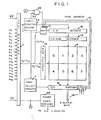
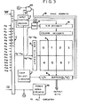
- Figs. 1, 2, and 3 are block diagrams of the circuit of the present invention mask programmed for three different page configurations, namely, eight pages of 128K bits each, four pages of 256K bits each, and a single page of 1KK bits, respectively.
- the illustrated paging configurations constitute examples of a larger variety of different possible paging configurations and are not to be considered a limitation on the present invention. These paging configurations are illustrated for purposes of explanation only.
- FIG. 1KK bit matrix array of storage devices generally designated A, preferably manufactured using a CMOS silicon gate process.
- the array is designed such that its output configuration is programmable.
- ROM A can generate either 8-bit or 16-bit output words through the data transfer circuit, generally designated B, which is connected thereto.
- the data transfer circuit B contains the required number of output buffers and controls the length of the output word.
- Data transfer circuit B is connected to the data bus 10.
- Data bus 10 serves to route data accessed from ROM A to the microprocessing unit of the system in which the circuit is employed.
- Data bus A also functions as an input for the page address signal generated by the microprocessing unit of the system, as explained below.
- ROM A The storage devices in ROM A are addressed by address circuitry which includes a conventional row decoder 12, a conventional column decoder 14, and a mask programmable page decoder 16.
- Row decoder 12 has, for example, ten outputs connected in parallel to each of the eight 128K pages in ROM A, designated on Fig . 1 as: "0, 1, 2, 3, 4, 5, 6, and 7".
- column decoder 14 has, for example, eight outputs connected in parallel to the sets of columns which form vertically aligned pages.
- Row decoder 12 receives its inputs directly from the output of an input buffer circuit, generally designated C.
- Column decoder 14 receives its inputs from page decoder 16 which, in turn, is connected to the output of a random access memory, generally designated D.
- RAM D is connected by means of parallel lines 18 to data transfer circuit B so as to receive the bits of the page address signal therefrom. It is also connected to the output of input buffer circuit C and to the output of a gate 20.
- Gate 20 receives, as one input, a command (write enable) signal (WE) from an input function decoder circuit, generally designated E.
- WE command (write enable) signal
- the output of the function generator E is also connected to decoder 16.
- gate 20 The other input of gate 20 is the Chip Enable ( CE ) signal which is an input to input buffer circuit C, which is also connected to the power down circuitry 22 of conventional design.
- CE Chip Enable
- Gate 20 causes all of the storage devices in the non-selected pages of ROM A to be in the low power mode.
- Circuit 22 controls the power status of other circuits in the system.
- Input buffer circuit C has, for example, seventeen address inputs denoted A 0 ...A 16 . It also has an input to receive the Chip Enable ( CE ) signal and an input to receive the command signal which is the-Write Enable signal ( WE ) from the microprocessing unit.
- the input buffer circuit C is mask programmable to block the path of selected ones of the address inputs A 0 ...A 16 , depending upon the page configuration. Only input buffer circuit C and decoder 16 need be mask programmed to define the page configuration of ROM A. All other components are identical, regardless of the page configuration.
- An output of input function decoder E is connected to a chip select circuit, generally designated F, which, in turn, is connected to data transfer circuit B.
- the chip select circuit F controls the data transfer circuit B to permit the page address signal on data bus 10 to be transferred to lines 18 in the presence of the command signal WE .
- decoder 16 is mask programmed to form a conventional 3:8 decoder, the three inputs being the three bits of the page address signal (P 0 , P 1 , P 2 ) which are present on data bus 10 and routed through data transfer circuit B by means of parallel lines 18 to RAM D.
- RAM D is a slow set up/hold RAM employed to insure temporary storage of the page address signal, which is generated by the system during the presence of the command signal WE . RAM D will retain the page address signal until the rising edge of the next WE signal.
- the WE signal and the page address signal (P 0 , P 1 , P 2 ) are generated by the microprocessing unit of the system in which the ROM circuit of the present invention is employed.
- Input buffer circuit C is mask programmed such that the paths of three of the address inputs, designated A 14 , A 151 A 16 are blocked. Thus, input buffer circuit C passes only address inputs A 0 -A 13 to the decoders.
- a 0 -A 9 are provided as inputs to row decoder 12.
- a 9 -A 13 are provided as inputs to RAM D, are routed through decoder 16 and along with the output of decoder 16, form the inputs to column decoder 14.
- the output of column decoder 14 causes the selection of the appropriate page and the appropriate column in that page. In conjunction with the output of row decoder 12, the appropriate location of the selected page is accessed and the data therein fed to data transfer circuit B.
- decoder 16 is mask programmed into two separate conventional decode circuits, a 1:2 decoder 16a, and a 2:4 decoder 16b. In this case, only a two-bit page address signal (P 0 , P 1 ) is required.
- the 2-bit page address signal passes through RAM D and is provided as the input to the 2:4 decoder 16b. This configuration is illustrated in Fig. 2.
- Input buffer circuit C is mask programmed to block the paths of address inputs A 15 and A 16 only. Unlike the previous example, the path of address input A 14 is not blocked. Inputs A o -A 14 are routed to the decoders, with inputs A 0 -A 9 being applied to row decoder 12 and inputs A 9 -A 14 providing an input for RAM D. Input A 14 is routed to the 1:2 decoder 16a and is used to select the "A" or "B" section of the selected one of four pages denoted as 0, 1, 2, and 3. The output of decoder 16a and decoder 16b, along with inputs A9-A13, are provided as inputs to column decoder 14. The outputs of decoder 14, in conjunction with the outputs of row decoder 12, serve to select the appropriate page, the appropriate page section, the appropriate column, and the appropriate row of the location to be accessed.
- the circuit of the present invention can also be mask programmed for use as a single page ROM having 1KK bits. No paging is required to access any data, as all locations are directly accessible. In this case, no paging signal is provided on data bus 10 and, thus, none is transferred to RAM D. All of the addressed inputs A 0 -A 16 to the input buffer are used and all are transferred to the decoders. Inputs A 0 -A 9 are provided to row decoder 12 and inputs A 9 -A 16 are provided to RAM D. RAM D is never enabled, it simply functions to transfer inputs A 9 -A 16 to decoder 16, which is a conventional 3:8 decoder.
- Inputs A14, A 159 and A 16 form the three inputs to decoder 16.
- the other inputs A9-A13, along with the output of decoder 16, are provided as inputs to column decoder 14.
- Column decoder 14, in conjunction with row decoder 12, directly accesses the particular storage unit desired.
- the command signal ( WE ) has no effect on the circuit as the circuit functions as a standard ROM without pagination.
- the circuit of the present invention can be adapted for use in a variety of different pagination modes by mask programming the peripheral circuitry, including the address decoder and input buffer circuit.
- the address decoder is mask programmed to form a selected one of conventional decoder configurations.
- the input buffer circuitry is mask programmed to block selected address input paths. This enables the circuit of the present invention to be used in a variety of pre-existing systems having fixed numbers of address inputs by adapting the system to generate the necessary page address signal on the data bus in the presence of the write enable command.
- the ROM circuit of the present invention is unique in that the data transfer circuit, aside from the usual data output function, also provides entrance for the page address signal and routes same to the decoder through a temporary storage circuit.
- the presence of the temporary storage circuit, in the form of a latch, preferably a random access memory, is in itself novel on a ROM circuit, as conventional ROM circuits have no facility for temporarily storing address signals. Such storage is required in the present invention such that page selection can be maintained as various locations within a particular page are accessed.
Landscapes
- Engineering & Computer Science (AREA)
- Microelectronics & Electronic Packaging (AREA)
- Read Only Memory (AREA)
Applications Claiming Priority (2)
| Application Number | Priority Date | Filing Date | Title |
|---|---|---|---|
| US06/757,337 US4744053A (en) | 1985-07-22 | 1985-07-22 | ROM with mask programmable page configuration |
| US757337 | 1985-07-22 |
Publications (3)
| Publication Number | Publication Date |
|---|---|
| EP0210064A2 true EP0210064A2 (de) | 1987-01-28 |
| EP0210064A3 EP0210064A3 (en) | 1989-07-26 |
| EP0210064B1 EP0210064B1 (de) | 1993-06-16 |
Family
ID=25047411
Family Applications (1)
| Application Number | Title | Priority Date | Filing Date |
|---|---|---|---|
| EP86305575A Expired - Lifetime EP0210064B1 (de) | 1985-07-22 | 1986-07-21 | Festwertspeicher mit veränderlicher Seite |
Country Status (5)
| Country | Link |
|---|---|
| US (1) | US4744053A (de) |
| EP (1) | EP0210064B1 (de) |
| JP (1) | JPS6265297A (de) |
| KR (1) | KR900008186B1 (de) |
| DE (1) | DE3688574D1 (de) |
Cited By (2)
| Publication number | Priority date | Publication date | Assignee | Title |
|---|---|---|---|---|
| EP0299697A2 (de) * | 1987-07-15 | 1989-01-18 | Hitachi, Ltd. | Integrierte Halbleiterschaltungsanordnung |
| US5257234A (en) * | 1987-07-15 | 1993-10-26 | Hitachi, Ltd. | Semiconductor integrated circuit device |
Families Citing this family (7)
| Publication number | Priority date | Publication date | Assignee | Title |
|---|---|---|---|---|
| US5231603A (en) * | 1985-07-22 | 1993-07-27 | Microchip Technology Incorporated | Variable page ROM |
| US4979148A (en) * | 1988-12-09 | 1990-12-18 | International Business Machines Corporation | Increasing options in mapping ROM in computer memory space |
| DE69020384T2 (de) * | 1989-02-27 | 1996-03-21 | Nec Corp | Integrierte Halbleiterspeicherschaltung mit Möglichkeit zum Maskieren des Schreibens im Speicher. |
| JPH02285442A (ja) * | 1989-04-27 | 1990-11-22 | Nec Corp | 半導体記憶装置 |
| US5485418A (en) * | 1990-01-16 | 1996-01-16 | Mitsubishi Denki Kabushiki Kaisha | Associative memory |
| US6005803A (en) * | 1998-09-23 | 1999-12-21 | Advanced Micro Devices, Inc. | Memory address decoding circuit for a simultaneous operation flash memory device with a flexible bank partition architecture |
| JP4257824B2 (ja) * | 2002-07-03 | 2009-04-22 | シャープ株式会社 | 半導体記憶装置 |
Citations (2)
| Publication number | Priority date | Publication date | Assignee | Title |
|---|---|---|---|---|
| EP0098755A2 (de) * | 1982-03-19 | 1984-01-18 | Fairchild Semiconductor Corporation | Programmierbares Adressenpuffer für Teilschaltungen |
| EP0115128A2 (de) * | 1982-12-04 | 1984-08-08 | Fujitsu Limited | Blockgeteilte Halbleiterspeicheranordnung |
Family Cites Families (5)
| Publication number | Priority date | Publication date | Assignee | Title |
|---|---|---|---|---|
| US3518631A (en) * | 1967-01-13 | 1970-06-30 | Ibm | Associative memory system which can be addressed associatively or conventionally |
| US4368515A (en) * | 1981-05-07 | 1983-01-11 | Atari, Inc. | Bank switchable memory system |
| US4480320A (en) * | 1982-06-01 | 1984-10-30 | General Instrument Corp. | Compact ROM with reduced access time |
| JPS59135695A (ja) * | 1983-01-24 | 1984-08-03 | Mitsubishi Electric Corp | 半導体記憶装置 |
| US4670858A (en) * | 1983-06-07 | 1987-06-02 | Tektronix, Inc. | High storage capacity associative memory |
-
1985
- 1985-07-22 US US06/757,337 patent/US4744053A/en not_active Expired - Lifetime
-
1986
- 1986-07-21 DE DE8686305575T patent/DE3688574D1/de not_active Expired - Lifetime
- 1986-07-21 EP EP86305575A patent/EP0210064B1/de not_active Expired - Lifetime
- 1986-07-22 KR KR1019860006000A patent/KR900008186B1/ko not_active IP Right Cessation
- 1986-07-22 JP JP61170951A patent/JPS6265297A/ja active Granted
Patent Citations (2)
| Publication number | Priority date | Publication date | Assignee | Title |
|---|---|---|---|---|
| EP0098755A2 (de) * | 1982-03-19 | 1984-01-18 | Fairchild Semiconductor Corporation | Programmierbares Adressenpuffer für Teilschaltungen |
| EP0115128A2 (de) * | 1982-12-04 | 1984-08-08 | Fujitsu Limited | Blockgeteilte Halbleiterspeicheranordnung |
Cited By (5)
| Publication number | Priority date | Publication date | Assignee | Title |
|---|---|---|---|---|
| EP0299697A2 (de) * | 1987-07-15 | 1989-01-18 | Hitachi, Ltd. | Integrierte Halbleiterschaltungsanordnung |
| EP0299697A3 (en) * | 1987-07-15 | 1990-12-05 | Hitachi, Ltd. | Semiconductor integrated circuit device |
| US5105389A (en) * | 1987-07-15 | 1992-04-14 | Hitachi, Ltd. | Semiconductor integrated circuit device |
| US5257234A (en) * | 1987-07-15 | 1993-10-26 | Hitachi, Ltd. | Semiconductor integrated circuit device |
| US5335204A (en) * | 1987-07-15 | 1994-08-02 | Hitachi., Ltd. | Semiconductor integrated circuit device |
Also Published As
| Publication number | Publication date |
|---|---|
| KR870001602A (ko) | 1987-03-14 |
| EP0210064A3 (en) | 1989-07-26 |
| JPH033318B2 (de) | 1991-01-18 |
| US4744053A (en) | 1988-05-10 |
| EP0210064B1 (de) | 1993-06-16 |
| KR900008186B1 (ko) | 1990-11-05 |
| JPS6265297A (ja) | 1987-03-24 |
| DE3688574D1 (de) | 1993-07-22 |
Similar Documents
| Publication | Publication Date | Title |
|---|---|---|
| US5717901A (en) | Variable depth and width memory device | |
| US7890694B2 (en) | Latched address multi-chunk write to EEPROM | |
| US4964078A (en) | Combined multiple memories | |
| US4523276A (en) | Input/output control device with memory device for storing variable-length data and method of controlling thereof | |
| CN1114927C (zh) | 存储器装置的冗余电路及其存取冗余地址的方法 | |
| US7995420B2 (en) | User selectable banks for DRAM | |
| EP1259963B1 (de) | Speicheranordnung mit unterstützung von nichtausgerichtetem zugriff | |
| US5150330A (en) | Interblock dispersed-word memory architecture | |
| US5854763A (en) | Integrated circuit with non-binary decoding and data access | |
| US4744053A (en) | ROM with mask programmable page configuration | |
| US5598365A (en) | High-density read-only memory | |
| EP0241078B1 (de) | Speicher mit gleichzeitig adressierbaren Speicherelementen | |
| US5231603A (en) | Variable page ROM | |
| KR890002773A (ko) | 디지탈 비데오 신호의 기억 장치 및 그 방법 | |
| US4040029A (en) | Memory system with reduced block decoding | |
| US5588133A (en) | Register block circuit for central processing unit of microcomputer | |
| US5737767A (en) | System for reconfiguring the width of an x-y RAM | |
| US4975882A (en) | User programmable redundant memory | |
| US6426913B1 (en) | Semiconductor memory device and layout method thereof | |
| US6407961B1 (en) | Dual access memory array | |
| US5873126A (en) | Memory array based data reorganizer | |
| US6781914B2 (en) | Flash memory having a flexible bank partition | |
| JPH0279294A (ja) | データ長変更可能メモリ | |
| US5276846A (en) | Fast access memory structure | |
| USRE38651E1 (en) | Variable depth and width memory device |
Legal Events
| Date | Code | Title | Description |
|---|---|---|---|
| PUAI | Public reference made under article 153(3) epc to a published international application that has entered the european phase |
Free format text: ORIGINAL CODE: 0009012 |
|
| AK | Designated contracting states |
Kind code of ref document: A2 Designated state(s): BE DE FR GB IT NL SE |
|
| PUAL | Search report despatched |
Free format text: ORIGINAL CODE: 0009013 |
|
| RHK1 | Main classification (correction) |
Ipc: G11C 8/00 |
|
| AK | Designated contracting states |
Kind code of ref document: A3 Designated state(s): BE DE FR GB IT NL SE |
|
| 17P | Request for examination filed |
Effective date: 19900109 |
|
| 17Q | First examination report despatched |
Effective date: 19910118 |
|
| GRAA | (expected) grant |
Free format text: ORIGINAL CODE: 0009210 |
|
| AK | Designated contracting states |
Kind code of ref document: B1 Designated state(s): BE DE FR GB IT NL SE |
|
| PG25 | Lapsed in a contracting state [announced via postgrant information from national office to epo] |
Ref country code: IT Free format text: LAPSE BECAUSE OF FAILURE TO SUBMIT A TRANSLATION OF THE DESCRIPTION OR TO PAY THE FEE WITHIN THE PRE;WARNING: LAPSES OF ITALIAN PATENTS WITH EFFECTIVE DATE BEFORE 2007 MAY HAVE OCCURRED AT ANY TIME BEFORE 2007. THE CORRECT EFFECTIVE DATE MAY BE DIFFERENT FROM THE ONE RECORDED.SCRIBED TIME-LIMIT Effective date: 19930616 Ref country code: SE Effective date: 19930616 Ref country code: DE Effective date: 19930616 Ref country code: BE Effective date: 19930616 Ref country code: FR Effective date: 19930616 Ref country code: NL Effective date: 19930616 |
|
| REF | Corresponds to: |
Ref document number: 3688574 Country of ref document: DE Date of ref document: 19930722 |
|
| PG25 | Lapsed in a contracting state [announced via postgrant information from national office to epo] |
Ref country code: GB Effective date: 19930916 |
|
| EN | Fr: translation not filed | ||
| NLV1 | Nl: lapsed or annulled due to failure to fulfill the requirements of art. 29p and 29m of the patents act | ||
| PLBE | No opposition filed within time limit |
Free format text: ORIGINAL CODE: 0009261 |
|
| STAA | Information on the status of an ep patent application or granted ep patent |
Free format text: STATUS: NO OPPOSITION FILED WITHIN TIME LIMIT |
|
| GBPC | Gb: european patent ceased through non-payment of renewal fee |
Effective date: 19930916 |
|
| 26N | No opposition filed | ||
| P01 | Opt-out of the competence of the unified patent court (upc) registered |
Effective date: 20230520 |