EP0209931A2 - Entzerrer mit steuerbaren Bandfiltern und digitaler Filter geeignet für Verwendung in einem Entzerrer - Google Patents
Entzerrer mit steuerbaren Bandfiltern und digitaler Filter geeignet für Verwendung in einem Entzerrer Download PDFInfo
- Publication number
- EP0209931A2 EP0209931A2 EP86201086A EP86201086A EP0209931A2 EP 0209931 A2 EP0209931 A2 EP 0209931A2 EP 86201086 A EP86201086 A EP 86201086A EP 86201086 A EP86201086 A EP 86201086A EP 0209931 A2 EP0209931 A2 EP 0209931A2
- Authority
- EP
- European Patent Office
- Prior art keywords
- filter
- frequency
- equaliser
- combination unit
- filters
- Prior art date
- Legal status (The legal status is an assumption and is not a legal conclusion. Google has not performed a legal analysis and makes no representation as to the accuracy of the status listed.)
- Granted
Links
Images


Classifications
-
- H—ELECTRICITY
- H03—ELECTRONIC CIRCUITRY
- H03H—IMPEDANCE NETWORKS, e.g. RESONANT CIRCUITS; RESONATORS
- H03H17/00—Networks using digital techniques
- H03H17/02—Frequency selective networks
- H03H17/0294—Variable filters; Programmable filters
-
- H—ELECTRICITY
- H03—ELECTRONIC CIRCUITRY
- H03G—CONTROL OF AMPLIFICATION
- H03G5/00—Tone control or bandwidth control in amplifiers
- H03G5/005—Tone control or bandwidth control in amplifiers of digital signals
-
- H—ELECTRICITY
- H03—ELECTRONIC CIRCUITRY
- H03G—CONTROL OF AMPLIFICATION
- H03G5/00—Tone control or bandwidth control in amplifiers
- H03G5/16—Automatic control
- H03G5/165—Equalizers; Volume or gain control in limited frequency bands
-
- H—ELECTRICITY
- H03—ELECTRONIC CIRCUITRY
- H03G—CONTROL OF AMPLIFICATION
- H03G5/00—Tone control or bandwidth control in amplifiers
- H03G5/16—Automatic control
- H03G5/18—Automatic control in untuned amplifiers
-
- H—ELECTRICITY
- H03—ELECTRONIC CIRCUITRY
- H03H—IMPEDANCE NETWORKS, e.g. RESONANT CIRCUITS; RESONATORS
- H03H17/00—Networks using digital techniques
- H03H17/02—Frequency selective networks
- H03H17/04—Recursive filters
Definitions
- the invention relates to an equaliser for varying the frequency characteristic of an electric signal presented to an input of the equaliser and for applying a frequency characteristic-adapted electric signal to an output, said equaliser comprising a plurality of band filters with their bands adjacent to one another in a given frequency range, the distance between the central frequencies of filters having neighbouring bands, being greater than the distance between the central frequencies of one third octave filters having neighbouring bands located at at least substantially the same frequencies as those of the band filters.
- the invention also relates to a band filter suitable for use in the equaliser.
- Equalisers of the type specified above ar known from British Patent Application GB 2,608,678A laid open to public inspection.
- Such an equaliser may be built up from, for example, a number of parallel arranged bandpass filters whose central frequencies are one octave apart. In this case each filter provides a substantially complete suppression outside the relevant band.
- Another possibility is for the equaliser to be built up from a number of series-arranged band filters. In the latter case each filter passes the signal unchanged outside the relevant band, that is to say, the gain is equal to fx. Within the relevant band the filter can amplify and then it functions as a bandpass filter, or attenuate and then it functions as a bandstop filter.
- the equaliser according to the invention is characterized in that the central frequencies of at least those band filters whose bands are located in the low-frequency part of the frequency range are variable.
- the invention is based on the recognition that in the case of equalisation using band filters whose central frequencies are fairly far apart, particularly at low frequencies, the location of these bands does not correspond to the location of peaks and dips in the frequency characteristic which is to be corrected. In fact, the location of these peaks and dips along the frequency axis is dependent on, inter alia, the position in the space of a loudspeaker box by means of which the acoustic signal is radiated into this space, and on the shape and size of the space.
- the band filters By rendering the central freqeuncies of the band filters variable in accordance with the invention, it is possible to adjust the filter bands along the frequency axis towards higher or lower frequencies until the bands correspond to the peaks and dips in the frequency characteristic to be corrected, whereafter a satisfactory equalisation is possible.
- the band filters can very easily be adjusted if they are constructed as digital filters. Each filter is then provided with an associated memory for storing as many sets of filter coefficients for the digital filter as are required for the different adjustments of the filters. To this end the output of each memory is coupled to a coefficient input of the associated band filter for the supply of a set of filter coefficients to the filter under the influence of a control signal applied to control inputs of the memory and of the filter.
- the central fre- q uencies of at least those band filters whose bands are in a low-frequency part of the frequency range will be made variable.
- the said low-frequency part can extend to about 1 kHz.
- the afore-mentioned problem could also be solved in another manner, for example by providing an equaliser with filters whose central frequencies are closer together, such as one third octave filters.
- An equaliser with filters whose central frequencies are closer together such as one third octave filters.
- a satisfactory e q ualisation is possible in this case.
- an equaliser with bands whose central frequencies are an octave apart for example octave bands
- three times as many filters are required, which is very expensive.
- the operation of such an equaliser is much more intricate.
- the central frequencies of those band filters which are located in the low-frequency part of the frequency range can be shifted towards lower and higher frequencies over a maximum of half heir distance from the central frequencies of neighbouring band filters, it is to be noted that this applies when the frequencies are plotted on a logarithmic scale.
- the central frequencies of the band filters in the non-shifted condition are at least separated over approximately the width of the octave and the central frequencies of the filters can be shifted ever the width of one third octave at a maximum. It is feasible that three positions are chosen on the frequency axis for the central frequency of a band, namely those positions corresponding to the central frequencies of the three one third octave bands around and/or in the relevant band.
- the memory contains three sets of filter coefficients for the three positions of the (digital) filter band on the frequency axis (in the case of an equal gain at the central frequency of the filter for the three situations),
- If the equaliser furthermore comprises
- the equaliser may be further characterized in that a band filter comprises a series arrangement of a first signal combination unit, a first delay means, a second signal combination unit and a second delay means, in that outputs of the two delay means are fed back to an input of the first signal combination unit and an input of the second signal combination unit, respectively, and in that the output of the second delay means is also fed back to an input of the first signal combination unit.
- Such a digital embodiment of a band filter may be further characterized in that the difference between the two coefficients corresponding to a first gain factor representing the loop gain in the circuit from the output of the first signal combination unit via the first delay means and the associated feedback to the first signal combination unit, and a second gain factor representing the loop gain in the circuit from the output of the second signal combination unit via the second delay means and the associated feedback to the second signal combination unit, is equal to the smallest unit in which these coefficients are expressed, and/or if the signs of the relevant coefficients are ignored, the difference between the two coefficients corresponding to a third gain factor representing the gain in the circuit from the output of the first signal combination unit via the first delay means to the input of the second signal combination unit and a fourth gain factor representing the gain in the circuit from the output of the second signal combination unit via the second delay means and the associated feedback to the input of the first signal combination unit is equal to the smallest unit in which these coefficients are expressed.
- Fig. 4.33 discloses a digital filter which has an input coupled to a series arrangement of a first signal combination unit, a first delay means, a second signal combination unit and a second delay means, the outputs of the first and second delay means being coupled via associated feedback paths to an input of the first signal combination and an input of the second signal combination unit, respectively, and the output of the second delay means being also fed back to an input of the fi.rst signal combination unit.
- the known filter comprises a coupled pole pair structure. This means that the two coefficients which correspond to the first and the second gain factor are equal. If their sign is ignored,the same applies to the two coefficients which correspond to the third and the fourth gain factor.
- the representation of the coefficients as a digital number for its supply to the digital filter implies that a rounding-off is generally effected because the digital number is always expressed in a limited number of bits. It is common practice to choose these digital numbers for the first and the second gain factor and for the third and the fourth gain factor to be equal as well. Using these digital numbers, the digital filter which is obtained will therefore only give an approximation of the desired filter characteristic.
- a better approximation to the desired filter characteristic is obtained, when in some cases the difference between the two coefficients corresponding to a first gain factor representing the loop gain in the circuit from the output of the first signal combination unit via the first delay means to the input of the second signal combination unit and a fourth gain factor representing the gain in the circuit from the output of the second signal combination unit via the second delay means and the associated feedback to the input of the first signal combination unit is equal to the smallest unit in which these coefficients are expressed.
- the foregoing implies that in some cases the digital representation of two coefficients which are equal in the known filter now differ from each other by the value of the least significant bit.
- Fig. 1 shows an equaliser 1 with n series-arranged band filters F 1 to F between the input 2 and the output 3.
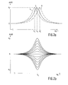
- the frequency characteristic of a band filter F i is represented by the curve 3 in Fig. 2a. Outside the band the filter has a gain which is equal to 1 x (OdB). Within the band it has a gain A i (in dB !).
- the central frequencies of neighbouring filters F i are more than one third octave apart, for example they are one octave apart.
- the central frequencies fc i of the filters F i (1 ⁇ i ⁇ n) are then, for example, at 31.5; 63; 125; 250 and 500 Hz; 1, 2, 4, 8 and 16 kHz.
- the band of filter F i (where 1 ⁇ i ⁇ m) can be shifted towards higher and lower frequencies over a maximum of half the distance to the central frequencies of the filters having neighbouring bands.
- the shift will preferably be limited to a maximum of the width of one third octave located in the band i in question.
- three settings of the filter F i are possible, namely the setting indicated by the curve 3; a second setting at which the filter characteristic (and hence the central frequency fc i of the filter) is shifted over the width of one third octave to lower frequencies (i.e.
- the bandwidth of the filters F i can be freely chosen but it should have the width of one third octave as a minimum.
- the width is preferably not taken to be larger than the width of one octave.
- the gain A is adjustable within the band. This is shown in Fig. 2b for the filter F i .
- the gain A is adjustable in a number of steps of, for example, 2 dB between a gain of 0 (dB) i.e. a gain of 1x and a gain of A i (dB).
- the filter may also attenuate and is adjustable between an attenuation of 0 (dB) and A i (dB) in the same number of steps of 2 dB.
- A 12 dB
- Fig. 2b thus comprises thirteen filter curves.
- the shifts of the characteristics of the filters F 1 up to and including F m along the frequency axis are controlled by control signals q 1 up to and including q m , respectively, and the gains/attenuations in the filters F 1 up to and including F n are controlled by control signals p 1 up to and including p n , respectively.
- the two control signals p i' q i (for q ⁇ i ⁇ m) and the control signal p i (for m ⁇ i ⁇ n) are/is to this end presented to the filter F i .
- this signal (these signals)ensure(s) an adjustment of the gain factor of the filter (and the adjustment of a frequency-determining element, for example, a variable coil, in the filter).
- control signal p i (the control signals p i' q i ) is (are) applied to memories M m+1 up to and including M n (the memories M 1 up to and including M m ), each memory M i being associated with a bandpass filter F i .
- FIG. 4 An embodiment of a digital filter is shown in Fig. 4, and Fi q . 5 shows the contents of the memory M i associated with bandpass filter F i .
- Fig. 4 shows an embodiment of a digital filter with which the filter characteristics of Fig. 2 can be realised.
- the input 20 is coupled via an amplifier stage 21 having a gain factor of k to an input of a signal combination unit 22.
- the output of the signal combination unit 22 is coupled to a series arrangement of a quantiser 23, a delay means 24 denoted by Z -1 , an amplifier stage 25 having a gain factor of b 1 , a second signal combination unit 26, a quantiser 27 and a second delay means 28.
- the outputs of the delay means 24 and 28 are fed back via amplifier stages 29 and 30 having gain factors of a 1 and a 2 , respectively, to inputs of the first and second signal combination units 22 and 26, respectively.
- the output of the delay means 28 is also fed back via an amplifier stage 31 having a gain factor of -b 2 to an input of the signal combination unit 22. Furthermore, the input 20 is coupled via delay means 32 and 33 and an amplifier stage 34 having a gain factor of -k to an input of the signal combination unit 22. Finally, the output of the delay means 32 and the output of the quantiser 27 are coupled to the output 36 via a signal combination unit 35.
- the elements 23 and 27 are quantisers which are commonly used in digital systems for reducing the data flow of digital numbers to the desired quantity of bits.
- quantisers reduce the numbers to, for example, 24 bits
- digital numbers having a length of 36 bits will be presented to the signal combination unit 26 as a result of the multiplication in, for example, the amplifier stage 25 in which the gain factor b 1 is represented, for example, by a 12-bit number.
- the quantiser 27 now reduces these 36-bit numbers to 24-bit digital numbers.
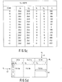
- Figs. 5a, 5b and 5c show the values of the coefficients al,a2, b 1 , b 2 and k corresponding again to the gain factors of the amplifier stages 29, 30, 25, 31 and 21 and 34 (the latter two having the value k), respectively, more specifically for the three central frequencies of 25 Hz, 31.5 Hz and 40 Hz and for different gains in the band.
- Fig. 5 actually shows the contents of the memory M 1 . If the control signal q 1 is such that the characteristic of filter F 1 must be set at a central frequency of 40 Hz and if the control signal p 1 is such that a gain of 4 dB is to be realised in the band, then it is evident from Fig.
- Fig. 5d diagrammatically shows the memory M 1 with three times thirteen sets of coefficients.
- the control signal q 1 selects that part of the memory M 1 which is associated with a given central frequency, i.e. the right-hand part in the afore-described example (see the arrow 41 which indicates that the control signal q 1 selects the part associated with 40 Hz), Subsequently the control signal p 1 selects the set of coefficients from the relevant part, which set is associated with a gain factor of 4 dB in accordance with the afore-mentioned example. This set of coefficients is diagrammatically denoted by means of the block 40. The arrow 43 indicates that the control signal p 1 selects the 4 dB gain.
- the memories M 2 to M m similarly contain the coefficients for the different amplifier stages in the filters F 2 to F m .
- the memories M m+1 to M n are smaller because they only need to contain the coefficients for one central frequency. This means that they only contain the 13 sets of coefficients associated with the central frequency fc i as is shown, for example, in Fig. 5b.
- the filter described in Fig. 4 is known in the art.
- the coefficients a 1 , a 2 can be calculated for a desired filter characteristic and are basically equal.
- the coefficients When the coefficients are to be subsequently represented digitally, they can be rounded off in the normal manner so that the digital representations of the coefficients a 1 and a 2 and b 1 , b 2 , respectively, are equal again.
- Fig. 5 shows that in some cases a 1 and a 2 or b 1 and b 2 are not equal. The reason is that in these cases the filter characteristic thus obtained approximates the desired filter characteristic better than in the case when a 1 and a 2 are equal and when b 1 and b 2 are equal.
- This value is between 2045.25 and 2045.75.
- a 1 is taken to be equal to 2045 and a 2 is 2046 (see Fig. 5a at the gain of 0 and 2 dB).
- a 1 could have been taken to be 2046 and a 2 could have been taken to be 2045.
- At the gain of 2 dB in Fig. 5a a different value for k would then have been obtained.
- the above described situations likewise apply to the coefficients b 1 and b 2 .
- the first two cases yield a band filter which is known in the art.
- a novel band filter is obtained realising a better approximation of the desired filter characteristic.
- the characteristic feature of this filter is that the coefficients a 1 and a 2 and/ or the coefficients b 1 and b 2 differ from each other by the value of 1x the least significant bit.
- Figs. 13a and b show the different filter characteristics obtained by means of the known calculation method (Fig. 13a - the coefficients a 1 and a 2 are equal to each other and the coefficients b 1 and b 2 are equal to each other) and by means of the calculation method as described hereinbefore (Fig. 13b in which for some sets of coefficients a 1 , a 2 , b1, b 2 these coefficients a 1 and a 2 or b 1 and b 2 differ from each other by the least significant bit).
- Fig. 13a For the purpose of clarification the vertical axis in Fig. 13a is slightly extended so that the variation of the characteristic curves in this Figure is more clearly visible. It is clear that the filter characteristics of Fig. 13b show a much greater resemblance to those of Fig. 2b than do the filter characteristics of Fig. 13a.
- the amplifier stage 29 in the circuit of Fig. 4 may be disposed in the circuit from the input of the signal combination unit 22 to the tapping point 37 for the feedback to the signal combination unit 22. If this is so,the gain factor a 1 still determines the gain in the circuit from the output of the first signal combination unit 22 via the delay means 24 and the associated feedback to the first signal combination unit 22. However, the gain factor for the amplifier stage 25 will then have to be changed to the value , in order that the gain in the circuit from the output of the first signal combination unit 22 via the delay means 24 to the input of the second signal combination unit 26 remains equal to b 1 . Another possibility is to dispose the amplifier stage 25 between the output of the signal combination unit 22 and the tapping point 37.
- the gain factor of the amplifier stage 29 will have to be modified to in order that the gain factor from the output of the signal combination unit 22 via the delay means 24 and the associated feedback to the first signal combination unit 22 remains equal to a 1 .
- Similar considerations apply to a displacement of the amplifier stage 30 or the amplifier stage 31 to within the circuit from the output of the signal combination unit 26 via the delay means 28 to the tapping point 38.
- a selection circuit 8 is provided which is coupled via the leads 11.1 to 11.n to charge inputs 7 of the respective band filters F 1 to F n . Via the leads 11.1 to 11.n one or more band filters can be selected for setting.
- the unit 9 supplies the control signals q 1 to q m via the lead 12 for setting the central frequencies of the filters F 1 to F m and the unit 10 supplies the control signals p 1 to p n via the lead 13 for setting the gain factors in the band filters F 1 to F n .
- the control signals p i (and q i for 1 ⁇ i ⁇ m) select an address in the memories M 1 to M n .
- the coefficients for the relevant setting of the digital filter are stored at this address in the memory, which coefficients are presented to the filters via the leads 14.1 to 14.n.
- a selection or charge signal presented via the charge inputs 7 to one or more of the filters then ensures that the new coefficients are stored in the filter, so that the filter is set again.
- the equaliser 1 of Fig. 1 is an example of a manually adjustable equaliser.
- the selection circuit 8 and the units 9 and 10 then have knobs (not shown) by means of which the selection of the filter, the setting of the central frequency of the filter and the setting of the gain factor of the filter can be adjusted.
- Fig. 6 shows an equaliser 60 with n parallel-arranged band filters G 1 to G n between the input 2 and the output 3.
- the outputs of the filters are coupled to the output 3 via an adder circuit 61.
- the frequency characteristic of a band filter G i is denoted by the curve 63 in Fig. 7. Outside the band the filter has a (very) large attenuation (that is to say, the gain factor of the filter is (very) much smaller than one there), Within the band the filter has a gain of roughly 1x.
- the distances between the central frequencies of neighbouring band filters is larger than one third octave again.
- the central frequencies of the filters G i in the embodiment of Fig. 6 are, for example, one octave apart again.
- the filters G 1 to G m are each adjustable at three positions on the frequency axis again, as is apparent from Fig. 7.
- the filter characteristic shifted towards lower frequencies over one third octave is denoted by the broken- line curve 64, with the central frequency fc i '.
- the dot-and dash line 65 shows the filter characteristic shifted towards higher frequencies over one third octave, with the central frequency fc i ".
- the value as stated in the Table of Fig. 3 can apply again to fc i , fc i ' and fc.”.
- the shift of the characteristics of the filters G 1 to G m along the frequency axis is controlled again by the control signals q 1 to q m which are supplied by the unit 9 through the lead 12.
- the gain factor a i of a filter G i is determined by the gain factor of an amplifier which is arranged in series with the filter. This is shown in Fig. 6 (only for the filter G 1 ). All filters G i may be constructed in this manner, the element 66 itself realising the filter characteristic which can be shifted along the frequency axis and the amplifier 67 ensuring the gain factor A 1 .
- the gain factor is controlled for each filter by means of the control signals p 1 to p n supplied by the unit 10 and directly controlling the amplifiers in the filters (such as the amplifier 67 in filter G 1 via the lead 13.
- the filters are constructed as digital filters
- the filters G 1 to G m have memories M 1 to M m with as many sets of coefficients being stored in each memory as are required for the (three) adjustments of the filters, that is to say, three sets.
- the signals q i are then address signals again, which select an address in the memory M i whereafter the contents of this address in the memory are presented to the filter (such as filter 66 in G 1 ) via the leads 14.1 to 14.m.
- the filter coefficients for the desired setting of the filter G i are then entered (only for those filters for which 1 i m:) via a charge signal which is generated by the selection circuit 8 and is presented via the lead 11.i to the charge input 7 of the filter G i , and the correct gain factor is set for the filter.
- the filter coefficients of the filters G m+1 to G n are fixed so that no memory for the storage of filter coefficients is required for these filters.
- the lower cut-off frequency of the filters F m+1 and G m+1 will preferably be made variable.
- Fig. 8a for the filter F m+1 and in Fi g. 8b for the filter G m+1'
- the lower band limit frequency being the -3 dB point at the frequency f 0
- the lower band limit frequency can be shifted towards lower frequencies, namely towards f 0 ' and towards higher frequencies, namely towards f 0 " dependent on the shift of the central frequency fc of the filters F m and G m , respectively.
- the position of the lower band limit frequency f 0 of the filters F m+1 and G m+1 may be coupled, for example, with the position of the central frequency fc m of the filters F m and G m in such a manner that in the case of a shift from fc to fc ' (that is, a shift towards lower freqeuncies) f 0 shifts towards f 0 ' and that in the case of a shift from fc to fc m " (that is, a shift towards higher frequencies) f 0 shifts towards f o " (thus also shifts towards higher frequencies).
- this can be manually set by operating the selection circuit 8 and the unit 9.
- the (manual) setting of the filters F m and G m may, however, also be coupled with the setting of the filters F m+1 and G m+1' respectively, so that in the case of a shift of the central frequency of the filters F and G , the lower cut-off frequency of the filters F m+1 and G m+1 , respectively, also shifts automatically with it.
- This is shown in Figs. 9 and 10.
- the filters in question with the variable lower band limit frequency are denoted by primed references in these Figures.
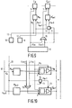
- Fig. 9 shows the relevant part of the embodiment of F ig. 1.
- the memory associated with the band filter F m+1 ' is different in this case, as has already been explained hereinbefore, and is therefore indicated by M m+1 '.
- the memory M m+1 ' now has the same structure and size as the memories M 1 to M m .
- this memory receives a control signal q m+1 for addressing.
- the selection signal 11.m+1 from the selection circuit 8 of Fig. 1 is applied via an OR-gate 70 to the charge input 7 of the band filter F m+1 '.
- the other input of the OR-gate 70 receives the selection signal 11.m.
- the selection signal 11.m+1 is also applied to a charge input 71 of a memory 72 in the lead 13 from the unit 10 to one control input of the memory M m+1 '.
- This memory 72 serves for storage of the control signal P m+1 for setting the gain in the filter F m+1 '.
- the operation of the circuit is as follows. When the filter F m+1 ' is selected via the selection circuit 8, that is to say, when a signal: logic "1" appears in the lead 11.m+1, both the lower band limit frequency of the filter F m+1 ' and the gain in the filter can be set by operating the units 9 and 10. Since the selection signal 11. m+1 is also applied to the charge input 71 of the memory 72, the control signal p m+1 is stored in this memory 72.
- the filter F m+1 ' is thus possible, independent of the setting of the filter F .
- the selection signal 11.m becomes a logic '1'.
- the filter F m can now be arbitrarily set by operating the units 9 and 10.
- the lower band limit frequency f 0 of the filter F m+1 ' is also adjusted simultaneously with the adjustment of the central frequency fc m of the filter F m , more specifically in such a manner that if fc m shifts towards fc m ', f o shifts towards f 0 ' and if fc m shifts towards fc m ", f 0 shifts towards f 0 ".
- the gain in the filter F m+1 ' then does not change, because the contents of the memory 72 determining the gain factor of the filter do not change.
- Fig. 10 shows the relevant part of the embodiment of Fi g . 6.
- the band filter G m+1 ' is also provided with a memory M m+1 .
- This memory comprises three sets of filter coefficients for the three adjustments of the lower cut-off frequency of the filter G M+1 '.
- the two selection signals 11.m and 11.m+1 are also applied via an OR-gate 70 to the charge input 7 of the filter G m+1 ' and a memory 72 is present in the lead 13 from the unit 10 to the control input 73 of the filter G m+1 ' for storing the control signal P m+1 at the command of the selection signal 11.m+1 which is presented to its charge input 71.
- the operation of the circuit of Fig. 10 is the same as that of Fig. 9.
- the filter characteristics of Figures 8a and b can be realised by arranging a high-pass filter and a low-pass filter in series with each other, the cut-off frequency of the high-pass filter being variable and the cut-off frequency of the low-pass filter being fixed.
- Fig. 11 diagrammatically shows an automatic equaliser.
- the equaliser for example the equaliser 1 of Fig. 1
- the equaliser 1 of Fig. 1 is also provided with an electro-acoustic converter unit in the form of a loudspeaker 80 disposed in a space 81.
- detection means for example, in the form of a microphone 82, which are coupled to an input 83 of a frequency analysing unit 84 are provided in the space.
- An input connection terminal 87 of the automatic equaliser is coupled to an input 85 of the frequency analysing unit 84.
- such circuits are generally known to equalise the acoustic signal radiated by the loudspeaker 80 into the space 81.
- a transfer function is derived in the analysing unit 84 whereafter a control signal 86 is derived by using the transfer function obtained, which control signal is applied to the equaliser 1 for setting the filters.
- the equaliser of Fig. 11 is different in the sense that a different control signal must be derived in the frequency analysing unit for controlling the equaliser 1.
- the frequency analysing unit 84 must generate the control signals p 1 to p n , q 1 to q m and the selection signals 11.1 to 11.n starting from the transfer function H (f) as obtained, for example, in the manner described in EP 119,645.
- the method implies that in the analysing unit 84 the previously mentioned transfer function H xy (f) is derived in amplitude and possibly also in phase and that a control signal is derived which is applied via the lead 86 to the equaliser 1. Under the influence of this control signal the equaliser realises a transfer function H xy -'(f) which in amplitude and possibly also in phase is the inverse of the transfer function H (f) as much as possible.
- the ananalysing unit 84 is to supply the coefficients for the digital filters so that the total transfer function H xy -'(f) in amplitude and possibly also in phase can be realised as satisfactorily as possible and can be approximated as optimally as possible.
- This optimum approximation can be realized for example, by means of known curve-fitting techniques using, for example, a least squares errors method for obtaining the optimum approximation of the inverse of the transfer function H xy (f).
- Fig. 12a shows an example of a transfer function H xy (f) obtained for a setting of the equaliser 1 which has a flat frequency characteristic.
- Fig. 12a only shows the amplitude transfer function in the low-frequency part of the total frequency range.
- the frequency analysing unit 84 has to supply such a control signal 86 to the equaliser 1 that a frequency characteristic is set in the equaliser 1 which is as much as possible the inverse of the characteristic H xy (f).
- F ig. 12b shows the location of the central frequencies fc 1 to fc 5 of the filters F 1 tp F 5 present in the low-frequency part.
- the transfer function in the low-frequency range for which there substantially applies that 20 f 700 Hz, roughly comprises five significant peaks and dips. These peaks and dips are denoted by f 1 to f 5 in Fig. 12a.
- the frequency analysing unit 84 then supplies such a control signal 86 that the peaks and dips in H xy (f) coincide as much as possible with the central frequencies of the filters F 1 to F 5 .
- the frequency analysing unit applies a control signal q 1 to filter F 1 , so that the central frequency shifts towards the value fc 1 ", applies control signals q 2 and q 3 to the filters F 2 and F 3 , respectively, so that the central frequencies remain in their place, and applies control signals q 4 and q 5 to the filters F 4 and F 5 , respectively, so that their central frequencies shift towards the values fc4' and fc 5 ', respectively.
- the frequency analysing unit m will apply such a control signal (p 1 , p 3 and p 5 ) to the filters F 1 , F 3 and F 5 that all three of them attenuate, that is to say, they have a gain factor of less than one, whilst the magnitude of the attnuation of course depends on the magnitude H xy (f) - H m at the frequencies f 1 , f 3 and f 5 .
- a control signal p 2 is applied to the filter F 2 such that it amplifies, that is to say, it has a gain factor of more than one, whilst the magnitude of the gain depends again on the magnitude H m -H x y(f) at the frequency f 2 .
- the frequency analysing unit 84 will present a control signal p 4 to the filter F 4 such that a gain factor of (approximately) 1x is set.
Landscapes
- Physics & Mathematics (AREA)
- Engineering & Computer Science (AREA)
- Computer Hardware Design (AREA)
- Mathematical Physics (AREA)
- Tone Control, Compression And Expansion, Limiting Amplitude (AREA)
- Circuit For Audible Band Transducer (AREA)
- Filters That Use Time-Delay Elements (AREA)
- Filters And Equalizers (AREA)
Applications Claiming Priority (2)
| Application Number | Priority Date | Filing Date | Title |
|---|---|---|---|
| NL8501834 | 1985-06-26 | ||
| NL8501834A NL8501834A (nl) | 1985-06-26 | 1985-06-26 | Egalisatie-inrichting met verschuifbare bandfilters en een digitaal filter eventueel te gebruiken in de egalisatie-inrichting. |
Related Child Applications (1)
| Application Number | Title | Priority Date | Filing Date |
|---|---|---|---|
| EP88202072.0 Division-Into | 1986-06-23 |
Publications (3)
| Publication Number | Publication Date |
|---|---|
| EP0209931A2 true EP0209931A2 (de) | 1987-01-28 |
| EP0209931A3 EP0209931A3 (en) | 1987-05-20 |
| EP0209931B1 EP0209931B1 (de) | 1990-01-31 |
Family
ID=19846196
Family Applications (1)
| Application Number | Title | Priority Date | Filing Date |
|---|---|---|---|
| EP86201086A Expired EP0209931B1 (de) | 1985-06-26 | 1986-06-23 | Entzerrer mit steuerbaren Bandfiltern und digitaler Filter geeignet für Verwendung in einem Entzerrer |
Country Status (5)
| Country | Link |
|---|---|
| US (1) | US4845758A (de) |
| EP (1) | EP0209931B1 (de) |
| JP (1) | JP2571215B2 (de) |
| DE (2) | DE3668737D1 (de) |
| NL (1) | NL8501834A (de) |
Cited By (3)
| Publication number | Priority date | Publication date | Assignee | Title |
|---|---|---|---|---|
| EP0571635A1 (de) * | 1991-11-28 | 1993-12-01 | Kabushiki Kaisha Kenwood | Anordnung zur Frequenzcharakteristikkorrektur eines Schallfeldes |
| US5541866A (en) * | 1991-11-28 | 1996-07-30 | Kabushiki Kaisha Kenwood | Device for correcting frequency characteristic of sound field |
| WO1997032397A1 (en) * | 1996-02-28 | 1997-09-04 | Ethymonics Limited | Digital filter |
Families Citing this family (20)
| Publication number | Priority date | Publication date | Assignee | Title |
|---|---|---|---|---|
| NL8501834A (nl) | 1985-06-26 | 1987-01-16 | Philips Nv | Egalisatie-inrichting met verschuifbare bandfilters en een digitaal filter eventueel te gebruiken in de egalisatie-inrichting. |
| JP3112913B2 (ja) * | 1989-12-28 | 2000-11-27 | パイオニア株式会社 | 音質調整装置 |
| AT397894B (de) * | 1990-05-08 | 1994-07-25 | Siemens Ag Oesterreich | Schaltungsanordnung zur entzerrung von digitalen tonsignalen |
| US5272656A (en) * | 1990-09-21 | 1993-12-21 | Cambridge Signal Technologies, Inc. | System and method of producing adaptive FIR digital filter with non-linear frequency resolution |
| US5524290A (en) * | 1991-07-22 | 1996-06-04 | Motorola, Inc. | Adaptive graphic equalizer and radio using same |
| US5268527A (en) * | 1991-11-25 | 1993-12-07 | Waller Jr James K | Audio power amplifier with reactance simulation |
| US5233665A (en) * | 1991-12-17 | 1993-08-03 | Gary L. Vaughn | Phonetic equalizer system |
| US20050259833A1 (en) * | 1993-02-23 | 2005-11-24 | Scarpino Frank A | Frequency responses, apparatus and methods for the harmonic enhancement of audio signals |
| US6275593B1 (en) | 1996-05-10 | 2001-08-14 | True Dimensional Sound, Inc. | Apparatus and methods for the harmonic enhancement of electronic audio signals |
| US5892833A (en) * | 1993-04-28 | 1999-04-06 | Night Technologies International | Gain and equalization system and method |
| US5559905A (en) * | 1993-09-22 | 1996-09-24 | Genesis Microchip Inc. | Digital image resizing apparatus |
| US6405227B1 (en) | 1998-12-31 | 2002-06-11 | New Japan Radio Co., Ltd. | Digital crossover and parametric equalizer |
| DE10143933A1 (de) * | 2001-09-07 | 2003-04-03 | Becker Gmbh 8 | Entzerreranordnung |
| US6876750B2 (en) * | 2001-09-28 | 2005-04-05 | Texas Instruments Incorporated | Method and apparatus for tuning digital hearing aids |
| US20030130751A1 (en) * | 2002-01-09 | 2003-07-10 | Freesystems Pte.,Ltd. | New filter bank for graphics equalizer implementation |
| US7333618B2 (en) * | 2003-09-24 | 2008-02-19 | Harman International Industries, Incorporated | Ambient noise sound level compensation |
| US7298206B2 (en) * | 2005-04-29 | 2007-11-20 | Tektronix, Inc. | Multi-band amplifier for test and measurement instruments |
| JP5445574B2 (ja) * | 2011-12-22 | 2014-03-19 | オンキヨー株式会社 | チャンネルデバイダおよびこれを含む音声再生システム、並びに、チャンネルデバイダのクロスオーバー周波数を設定する方法 |
| US9735751B1 (en) | 2012-01-09 | 2017-08-15 | Skullcandy, Inc. | Audio reproduction device target sound signature |
| CN111630873B (zh) * | 2018-01-04 | 2022-06-14 | 美商楼氏电子有限公司 | 传感器装置和麦克风组件 |
Citations (4)
| Publication number | Priority date | Publication date | Assignee | Title |
|---|---|---|---|---|
| GB2068678A (en) * | 1980-01-04 | 1981-08-12 | Dbx | Equalizing system |
| US4403201A (en) * | 1980-03-24 | 1983-09-06 | Nippon Gakki Seizo Kabushiki Kaisha | Bandpass filter circuit |
| EP0090464A1 (de) * | 1982-03-31 | 1983-10-05 | Koninklijke Philips Electronics N.V. | Digitale Klangregeleinrichtung |
| EP0119645A1 (de) * | 1983-02-23 | 1984-09-26 | Koninklijke Philips Electronics N.V. | Automatisches Entzerrungssystem mit diskreter Fourier-Transformation (DFT) oder schneller Fourier-Transformation (FFT) |
Family Cites Families (7)
| Publication number | Priority date | Publication date | Assignee | Title |
|---|---|---|---|---|
| US4206417A (en) * | 1978-06-22 | 1980-06-03 | Bose Corporation | Sound system control |
| US4271398A (en) * | 1978-11-30 | 1981-06-02 | Pioneer Electronic Corporation | Tone control device |
| US4484345A (en) * | 1983-02-28 | 1984-11-20 | Stearns William P | Prosthetic device for optimizing speech understanding through adjustable frequency spectrum responses |
| JPS6014514A (ja) * | 1983-07-05 | 1985-01-25 | Matsushita Electric Ind Co Ltd | グラフイツクイコライザ装置 |
| JPS60244111A (ja) * | 1984-05-18 | 1985-12-04 | Nec Corp | デイジタルフイルタ回路 |
| US4633501A (en) * | 1985-04-15 | 1986-12-30 | Werrbach Donn R | Program dependent crossover filter (PDC) |
| NL8501834A (nl) | 1985-06-26 | 1987-01-16 | Philips Nv | Egalisatie-inrichting met verschuifbare bandfilters en een digitaal filter eventueel te gebruiken in de egalisatie-inrichting. |
-
1985
- 1985-06-26 NL NL8501834A patent/NL8501834A/nl not_active Application Discontinuation
-
1986
- 1986-06-23 DE DE8686201086T patent/DE3668737D1/de not_active Expired - Lifetime
- 1986-06-23 DE DE88202072T patent/DE3689047T2/de not_active Expired - Fee Related
- 1986-06-23 EP EP86201086A patent/EP0209931B1/de not_active Expired
- 1986-06-26 US US06/878,933 patent/US4845758A/en not_active Expired - Fee Related
- 1986-06-26 JP JP61148314A patent/JP2571215B2/ja not_active Expired - Lifetime
Patent Citations (4)
| Publication number | Priority date | Publication date | Assignee | Title |
|---|---|---|---|---|
| GB2068678A (en) * | 1980-01-04 | 1981-08-12 | Dbx | Equalizing system |
| US4403201A (en) * | 1980-03-24 | 1983-09-06 | Nippon Gakki Seizo Kabushiki Kaisha | Bandpass filter circuit |
| EP0090464A1 (de) * | 1982-03-31 | 1983-10-05 | Koninklijke Philips Electronics N.V. | Digitale Klangregeleinrichtung |
| EP0119645A1 (de) * | 1983-02-23 | 1984-09-26 | Koninklijke Philips Electronics N.V. | Automatisches Entzerrungssystem mit diskreter Fourier-Transformation (DFT) oder schneller Fourier-Transformation (FFT) |
Non-Patent Citations (2)
| Title |
|---|
| AUDIO ENGINEERING SOCIETY PREPRINT, no. 843(E-2), 42nd Convention, May 2-5, 1972, pages 1-10 and figures; New York, US G.R. THURMOND: "New techniques for sound system equalization." * |
| ELEKTOR, vol. 5, no. 9; September 1979, pages 26-33; Canterburry, GB "Parametric equaliser" * |
Cited By (4)
| Publication number | Priority date | Publication date | Assignee | Title |
|---|---|---|---|---|
| EP0571635A1 (de) * | 1991-11-28 | 1993-12-01 | Kabushiki Kaisha Kenwood | Anordnung zur Frequenzcharakteristikkorrektur eines Schallfeldes |
| EP0571635A4 (en) * | 1991-11-28 | 1994-06-15 | Kenwood Corp | Device for correcting frequency characteristic of sound field |
| US5541866A (en) * | 1991-11-28 | 1996-07-30 | Kabushiki Kaisha Kenwood | Device for correcting frequency characteristic of sound field |
| WO1997032397A1 (en) * | 1996-02-28 | 1997-09-04 | Ethymonics Limited | Digital filter |
Also Published As
| Publication number | Publication date |
|---|---|
| EP0209931B1 (de) | 1990-01-31 |
| JP2571215B2 (ja) | 1997-01-16 |
| US4845758A (en) | 1989-07-04 |
| EP0209931A3 (en) | 1987-05-20 |
| DE3689047D1 (de) | 1993-10-21 |
| DE3668737D1 (de) | 1990-03-08 |
| DE3689047T2 (de) | 1994-04-07 |
| NL8501834A (nl) | 1987-01-16 |
| JPS621307A (ja) | 1987-01-07 |
Similar Documents
| Publication | Publication Date | Title |
|---|---|---|
| EP0209931B1 (de) | Entzerrer mit steuerbaren Bandfiltern und digitaler Filter geeignet für Verwendung in einem Entzerrer | |
| US5384856A (en) | Acoustic system | |
| CA2098190C (en) | Compensating filters | |
| US4980914A (en) | Sound field correction system | |
| EP1017166B1 (de) | Vorrichtung zur Veränderung akustischer Eigenschaften | |
| EP0219865B1 (de) | System und Verfahren zum Überwachen der Tonqualität | |
| US6721428B1 (en) | Automatic loudspeaker equalizer | |
| US4888811A (en) | Loudspeaker device | |
| JP4402977B2 (ja) | 補聴器における動的圧縮 | |
| JPH06141399A (ja) | サウンドイメージ高揚のための信号処理装置 | |
| JP2730860B2 (ja) | 音響信号の線形歪補償方法及びその装置 | |
| CN106162432A (zh) | 一种音频处理器装置及其声音补偿架构处理实现方法 | |
| KR0129429B1 (ko) | 오디오신호처리장치 | |
| US5737254A (en) | Symmetrical filtering apparatus and method therefor | |
| JP3557236B2 (ja) | オーディオ信号のデジタル処理回路装置 | |
| US7352872B2 (en) | Filter circuit and method for processing an audio signal | |
| JPH08107322A (ja) | 伝送特性制御回路 | |
| JPH02113613A (ja) | 音質調整装置 | |
| US11563425B2 (en) | Linear-phase fir audio filter, production method and signal processor | |
| JP3120394B2 (ja) | トーンコントロール回路 | |
| JPH05175773A (ja) | オーディオイコライザ | |
| JP3445909B2 (ja) | オーディオ装置及びその音量調整方法 | |
| US11539339B2 (en) | Audio signal processing method and apparatus for frequency spectrum correction | |
| KR102172489B1 (ko) | 크로스오버 네트워크, 이를 이용한 멀티웨이 스피커 시스템 및 오디오 시스템과 크로스오버 네트워크의 주파수 분할방법 | |
| JPH05292600A (ja) | 車載用音場補正装置 |
Legal Events
| Date | Code | Title | Description |
|---|---|---|---|
| PUAI | Public reference made under article 153(3) epc to a published international application that has entered the european phase |
Free format text: ORIGINAL CODE: 0009012 |
|
| AK | Designated contracting states |
Kind code of ref document: A2 Designated state(s): DE FR GB |
|
| PUAL | Search report despatched |
Free format text: ORIGINAL CODE: 0009013 |
|
| AK | Designated contracting states |
Kind code of ref document: A3 Designated state(s): DE FR GB |
|
| 17P | Request for examination filed |
Effective date: 19871103 |
|
| 17Q | First examination report despatched |
Effective date: 19880725 |
|
| GRAA | (expected) grant |
Free format text: ORIGINAL CODE: 0009210 |
|
| AK | Designated contracting states |
Kind code of ref document: B1 Designated state(s): DE FR GB |
|
| REF | Corresponds to: |
Ref document number: 3668737 Country of ref document: DE Date of ref document: 19900308 |
|
| ET | Fr: translation filed | ||
| PLBE | No opposition filed within time limit |
Free format text: ORIGINAL CODE: 0009261 |
|
| STAA | Information on the status of an ep patent application or granted ep patent |
Free format text: STATUS: NO OPPOSITION FILED WITHIN TIME LIMIT |
|
| 26N | No opposition filed | ||
| REG | Reference to a national code |
Ref country code: FR Ref legal event code: CD |
|
| PGFP | Annual fee paid to national office [announced via postgrant information from national office to epo] |
Ref country code: GB Payment date: 19970602 Year of fee payment: 12 |
|
| PGFP | Annual fee paid to national office [announced via postgrant information from national office to epo] |
Ref country code: FR Payment date: 19970624 Year of fee payment: 12 |
|
| PGFP | Annual fee paid to national office [announced via postgrant information from national office to epo] |
Ref country code: DE Payment date: 19970822 Year of fee payment: 12 |
|
| PG25 | Lapsed in a contracting state [announced via postgrant information from national office to epo] |
Ref country code: GB Free format text: LAPSE BECAUSE OF NON-PAYMENT OF DUE FEES Effective date: 19980623 |
|
| GBPC | Gb: european patent ceased through non-payment of renewal fee |
Effective date: 19980623 |
|
| PG25 | Lapsed in a contracting state [announced via postgrant information from national office to epo] |
Ref country code: FR Free format text: LAPSE BECAUSE OF NON-PAYMENT OF DUE FEES Effective date: 19990226 |
|
| PG25 | Lapsed in a contracting state [announced via postgrant information from national office to epo] |
Ref country code: DE Free format text: LAPSE BECAUSE OF NON-PAYMENT OF DUE FEES Effective date: 19990401 |
|
| REG | Reference to a national code |
Ref country code: FR Ref legal event code: ST |