EP0205936A2 - Semiconductor integrated circuit - Google Patents
Semiconductor integrated circuit Download PDFInfo
- Publication number
- EP0205936A2 EP0205936A2 EP86106972A EP86106972A EP0205936A2 EP 0205936 A2 EP0205936 A2 EP 0205936A2 EP 86106972 A EP86106972 A EP 86106972A EP 86106972 A EP86106972 A EP 86106972A EP 0205936 A2 EP0205936 A2 EP 0205936A2
- Authority
- EP
- European Patent Office
- Prior art keywords
- mosfets
- switch
- constructed
- address
- signals
- Prior art date
- Legal status (The legal status is an assumption and is not a legal conclusion. Google has not performed a legal analysis and makes no representation as to the accuracy of the status listed.)
- Granted
Links
Images


Classifications
-
- G—PHYSICS
- G11—INFORMATION STORAGE
- G11C—STATIC STORES
- G11C11/00—Digital stores characterised by the use of particular electric or magnetic storage elements; Storage elements therefor
- G11C11/21—Digital stores characterised by the use of particular electric or magnetic storage elements; Storage elements therefor using electric elements
- G11C11/34—Digital stores characterised by the use of particular electric or magnetic storage elements; Storage elements therefor using electric elements using semiconductor devices
- G11C11/40—Digital stores characterised by the use of particular electric or magnetic storage elements; Storage elements therefor using electric elements using semiconductor devices using transistors
-
- G—PHYSICS
- G11—INFORMATION STORAGE
- G11C—STATIC STORES
- G11C8/00—Arrangements for selecting an address in a digital store
- G11C8/10—Decoders
Definitions
- This invention relates to a semiconductor integrated circuit, and concerns a technique which is effective for use in a semiconductor integrated circuit comprising a decoder circuit, for example, a semiconductor memory.
- an address decoder which forms select signals for selecting memory cells is provided.
- the address decoder receives address signals of, e. g., n bits and forms one select signal in accordance with 2 combinations of the address signals.
- an address decoder can be constructed of a plurality of unit decoders each of which comprises a NOR gate circuit and a NAND gate circuit.
- each gate circuit requires (n + 1) MOSFETs.
- each gate circuit is constructed of a CMOS circuit composed of P-channel MOSFETs and N-channel MOSFETs, as many MOSFETs as 2n are required per gate circuit.
- the large number of elements are needed. This has now become a serious obstacle to attaining a higher integration density and a larger memory capacity of the semiconductor memory.
- the number of elements is reduced by utilizing a switch tree decode construction.
- the number of MOSFETs increases double as the branch of a tree spreads, and whereas smaller numbers of MOSFETs are arranged near the base point of the tree, the number of MOSFETs to be disposed on the distal end side of the tree is enlarged in the extreme.
- the gates of the large number of MOSFETs are connected in common to an input signal line for the MOSFETs on the distal end side.
- input gate capacitances and parasitic capacitances of large capacitance values are coupled to the input signal line.
- Such undesired capacitances retard the change of the input signal of the MOSFET on the distal end side, in other words, they retard the switching operation of the MOSFET, so that a higher speed operation cannot be achieved.
- An object of this invention is to provide a semiconductor integrated circuit which includes a decoder circuit having realized a simplified circuit arrangement and a raised operating speed.
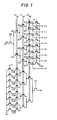
- Fig. 1 shows a circuit diagram of an address decoder in the first embodiment of this invention.
- Various circuit elements in the figure are formed on a single semiconductor substrate such as single-crystal silicon by the known manufacturing techniques of CMOS (complementary MOS) integrated circuits.
- CMOS complementary MOS
- an integrated circuit is formed on a semiconductor substrate which is made of single-crystal N-type silicon.
- a P-channel MOSFET is constructed of a P-type source region and a P-type drain region which are formed in the surface of such a semiconductor substrate, and a gate electrode made of, e. g., polycrystalline silicon which is formed on the part of the semiconductor substrate surface between such source and drain regions through a thin gate insulator film.
- An N-channel MOSFET is formed on a P-type well region which is formed in the semiconductor substrate surface.
- the respective MOSFETs are produced by the so-called self-alignment technique in which the gate electrodes made of polycrystalline silicon as stated above are employed as a kind of impurity introducing mask.
- the semiconductor substrate forms the common substrate gate of a plurality of P-channel MOSFETs formed thereon.
- the P-type well region forms the substrate gate of the N-channel MOSFET formed thereon.
- the substrate gate of the P-channel MOSFETs, namely, the N-type substrate is maintained at the supply voltage level of the circuit, while the body gate of the N-channel MOSFET, namely, the P-type well region is maintained at the ground potential of the circuit.
- the address decoder in the figure is formed on the semiconductor substrate along with an address buffer, not shown, which produces address signals a0 thru a3 of true level and address signals a0 thru a3 of false level in response to address signals A0 thru A3 respectively.
- the address signals of the complementary levels such as the address signals a0 and a0 shall be termed the complementary address signals.
- the illustrated address decoder forms 16 decoded outputs XO - X15 on the basis of the complementary address signals a0, aO - a3, a3 of 4 bits.
- the complementary address signals a3 and a3 are regarded as the most significant bit-address signals, and those a0 and a0 as the least significant bit-address signals.
- the address signal a3 of the inverted or false level at the most significant bit is supplied to the gate of a MOSFET Q24 whose source is coupled to the ground potential point of the circuit.
- the drain thereof is provided with two MOSFETs Q22 and Q23 which constitute a first branch.
- the gates of these two MOSFETs Q22 and Q23 are respectively supplied with the inverted address signal a2 and the address signal a2 of the non-inverted or true level.
- the drains of the two MOSFETs Q22 and Q23 are respectively provided with two MOSFETs Q18, Q19 and Q20, Q21 which constitute second branches.
- the gates of the two MOSFETs Q18, Q19 or Q20, Q21 are respectively supplied with the inverted address signal al and the non-inverted address signal al.
- the drains of the two MOSFETs Q18, Q19 and Q20, Q21 are respectively provided with two MOSFETs Q10 and Qll, Q12 and Q13, Q14 and Q15, and Q16 and Q17 which constitute third branches.
- the gates of these two MOSFETs Q10 and Qll, Q12 and Q13, Q14 and Q15, and Q16 and Q17 are respectively supplied with the inverted address signal a0 and the non-inverted address signal a0. All of the above MOSFETs Q10 - Q24 are N-channel MOSFETs.
- Load means which is constructed of P-channel MOSFETs Ql - Q8 though not especially restricted, is disposed between the drains of the MOSFETs Q10 - Q17 of the final branches and the supply voltage V .
- These MOSFETs Ql - Q8 operate as resistance elements in such a way that their gates are steadily supplied with the ground potential of the circuit.
- the MOSFETs Ql - Q24 mentioned above constitute a first group of MOSFETs. Eight of the decoded output signals, XO - X7 are delivered from the drains of the MOSFETs Q10 - Q17 of the final branches.
- decoded output signals XO - X7 ones selected according to the combination of the 4-bit address signals are made a low level such as the ground potential of the circuit, and non-selected output signals are made a high level such as the supply voltage V cc . More specifically, if all the inverted address signals aO - a3 are at the high level, the MOSFETs Q10, Q18, Q22 and Q24 are responsively brought into 'on' states, and hence, only the decoded output signal XO is made the selection level of the low level.
- decoded outputs Xl - X7 (and X8 - X15 to be described later) are all made the non-selection level of the high level (V ) because any MOSFETs in series therewith are brought into 'off' states by the low level of the non-inverted address signals aO - a3.
- the decoded output signals XO - X7 are inverted by driver circuits not shown, constructed of CMOS inverter circuits or the like and are then transmitted to the word lines of a memory array or the gates of column switch MOSFETs not shown, arranged on the right of the illustrated decoder.
- the remaining decoded output signals X8 - X15 are formed by a second group of MOSFETs which take a switch tree configuration similar,to the above.
- the MOSFET at a base point is supplied with the non-inverted address signal a3, and the MOSFETs at branch points to be supplied with the remaining complementary address signals a0, a0 - a2 , a2 are different. More specifically, - the gates of the MOSFETs of the first branch in the switch tree of this second group are supplied with the complementary address signals a0, a0 which are fed to the MOSFETs at the final branch points in the first group.
- the gates of the MOSFETs of the second branches in the switch tree of the second group are supplied with the complementary address signals al, al which are fed to the MOSFETs at the second branch points in the first group.
- the gates of the MOSFETs of the final (third) branches in the switch tree of the second group are supplied with the complementary address signals a2, a2 which are fed to the MOSFETs of the first branch points in the first group.
- the MOSFETs have the gates supplied with the corresponding complementary address signals symmetrically with respect to the intermediate second branches (the complementary address signals al, al).
- the MOSFETs located near the root of the switch tree such as the MOSFETs Q24, Q22 and Q23 may be arranged within the pitch of the plurality of MOSFETs Q10 thru Q17 constituting the final switch branches, and hence, they may be respectively fabricated with comparatively large sizes.
- a MOSFET of large size however, has a great gate capacitance or input capacitance. In the presence of such a great capacitance, the varying rate of an address signal applied to an address input line is drastically limited, and a transient current for charging or discharging such a capacitance is inevitably set at a comparatively high level. The transient current is caused to flow to the power source wiring or ground wiring of the circuit through the address buffer not shown. When the transient current is great, comparatively great noise appears in the power source wiring or the ground wiring.
- the MOSFETs such as those Ql thru Q24 constituting the switch trees have sizes equal to one another. That is, notwithstanding that the MOSFETs Q18 thru Q24 can be made larger in size than those Q10 thru Q17, they are fabricated with comparatively small sizes. Accordingly, capacitances to be coupled to the respective address input lines become small, and the varying rates of the corresponding address signals become high.
- the address input lines are constructed of polycrystalline silicon layers which are integral with the gate electrodes of the MOSFETs constituting the switch tree.
- the wiring between the MOSFETs constituting the switch tree for example, the wiring between the drain of the MOSFET Q24 and the sources of the MOSFETs Q22 and Q23 may be constructed of the so-called semiconductor interconnection region which is formed simultaneously with the drain and the sources. In this embodiment, however, such wiring is constructed .of an aluminum layer as a first layer interconnection which is formed on the semiconductor substrate through a first interlayer insulator film. Thus, a capacitance and a wiring resistance in a wiring part for the mutual coupling of the MOSFETs are reduced.
- Output wiring lines X0 thru X15 can be constructed of the first layers of aluminum layers. Output wiring lines X8 thru X15 are extended toward the memory array across a MOSFET forming area for constructing the switch tree.
- the address input lines made of the polycrystalline silicon layers have comparatively high resistances.
- a second interlayer insulator film and second aluminum interconnection layers may be formed.
- the second layers of aluminum interconnection layers are caused to intersect the first layers of aluminum interconnection layers through the second interlayer insulator film, and are held in contact with the polycrystalline silicon layers through proper contact holes.
- each of the address signals a0 and a0 of the least significant bit is fed to the gates of the five MOSFETs
- each of the address signals al and al of the second bit is fed to the gates of the four MOSFETs
- each of the address signals a2 and a2 of the third bit is fed to the gates of the five MOSFETs similarly to the least significant bit signals a0 and aO.
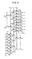
- Fig. 2 shows a circuit diagram of an address decoder in the second embodiment of this invention.
- the wiring for the coupling between the MOSFET of the base point and the MOSFETs of the first branch has a great wiring length because the tree spreads successively.
- the wiring is constructed of an aluminum interconnection or a semiconductor interconnection layer such as a diffused layer which is formed integrally with the source or drain of the MOSFET.
- the long wiring forms a cause for hampering enhancement in the operating speed of the decoder.
- the wiring length is shortened in such a way that, for example, the MOSFET of the base point in the switch tree of the first group is divided in two, MOSFETs Q24 and Q24'. This measure applies also to the switch tree of the second group.
- the wiring length on the base point side can be shortened, so that a raised speed of the operation can be attained.
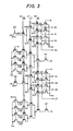
- Fig. 3 shows a circuit diagram of an address decoder in the third embodiment of this invention.
- each of the switch trees of the first and second groups can be divided in two and that the whole configuration forming the divided switch tree is triangular.
- the half switch tree in the switch tree of the second group is arranged in adjacency to the half switch tree in the switch tree of the first group. Owing to such a construction, the triangles made smaller by the division can be arranged in axial symmetry, and hence, the MOSFETs constituting the address decoder can be laid out at a higher density.
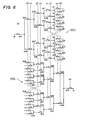
- Fig. 4 shows a circuit diagram of an address decoder in the fourth embodiment of this invention.
- the address decoder circuit is divided in two as a whole.
- Input signals to be supplied to the illustrated switch trees consist of four sorts of input signals AO - A3, BO - B3 and CO - C3 formed by a pre-decoder circuit (not shown) which decodes address signals each being composed of 2 bits.
- Each of the input signals AO thru A3 is formed of address signals of 2 bits.
- the input signal AO is put to a level "1" when the 2-bit address signals are "00”
- the input signal A3 is put to the level "1" when the 2-bit address signals are "11".
- the input signals Al and A2 are put to the level "1" when the 2-bit address signals are "01" and "10", respectively.
- each of the input signals BO thru B3 and CO thru C3 has its level determined by the 2-bit address signals.
- the switch trees have the MOSFETs of the base points and the first branches divided by a construction similar to that of the embodiment in Fig. 3, and the divided switch trees of the first and second groups are alternately arranged. Since the four sorts of pre-decoded signals are supplied as the input signals as described above, four MOSFETs are disposed at the branch point.
- the number of branch stages can be reduced.
- the number of driving MOSFETs to be connected in series with load MOSFETs can be lessened, so that a raised speed operation can be realized.
- the pre-decoder circuit has the small number of input bits, it may well be constructed of NOR or NAND gate circuitsor the like.
- Fig. 5 is a circuit diagram of a fifth embodiment.
- a pre-decoder circuit PRDEC is constructed of NOR circuits Gl thru G4 and inverter circuits IV1 thru IV4.
- Decoder circuits of the switch tree construction, STD1 thru STD4 are constructed similarly to the decoder circuit in Fig. 1.
- a MOSFET corresponding to the MOSFET Q24 in Fig. 1 is not provided.
- the output wiring line AO of the pre-decoder circuit PRDEC is coupled to sources like those of the MOSFETs Q22 and Q23 in Fig. 1. Therefore, the MOSFET corresponding to the MOSFET Q24 may be regarded as being replaced with a unit decoder circuit in the pre-decoder circuit PRDEC, in other words, the NOR circuit Gl and the inverter circuit IV1.
- the outputs XO thru X15 of the decoder circuits STD1 thru STD4 are supplied to a word line driving circuit WD which is constructed of inverter circuits IV5 thru IV12.
- the outputs of the word line driving circuit WD are supplied to the word lines WO thru W15 of a memory array MA which is constructed of static memory cells (not shown).
- the number of MOSFETs to be connected in series within the decoder circuits STD1 thru STD4 can be lessened.
- the ground wiring line to be coupled to the source of the MOSFET Q24 in Fig. 1 is replaced with the output wiring lines AO thru A3 of the pre-decoder PRDEC. It is therefore possible to lessen the number of total wiring lines for the decoder circuit.
- Fig. 6 is a circuit diagram of a decoder circuit in a sixth embodiment.
- a switch tree portion STD1 which is constructed of switching elements Ql thru Q31
- address input lines a0, a0 and al, al are exchanged as shown in the figure.
- a switch tree portion STD2 which is constructed of switching elements Q40 thru Q70
- address input lines a2, a2 and a3, a3 are exchanged.
- the switching elements Q1 thru Q31 and Q40 thru Q70 are made up of MOSFETs as in the preceding embodiments.
- the address input lines are exchanged within each switch tree portion, with the result that the numbers of the switching elements to be coupled to the-respective address input lines can be favorably averaged.
- the load means of a switch tree may well be constructed of MOSFETs of the same conductivity type as that of MOSFETs constituting the switch tree or utilize polycrystalline silicon resistors or the like, or they may well be constructed of a dynamic circuit employing precharging MOSFETs.
- pre-decoded outputs may well be supplied to only specified branch points.
- a plurality of columns of decoders may well be driven by common decoder signals.
- This invention is extensively applicable, not only to a semiconductor memory such as a dynamic RAM, a static RAM or any of various ROMs ,but also to various semiconductor integrated circuits each comprising a decoder circuit which receives digital signals composed of a plurality of (n) bits and forms 1/2 n decoded signals.
Abstract
Description
- This invention relates to a semiconductor integrated circuit, and concerns a technique which is effective for use in a semiconductor integrated circuit comprising a decoder circuit, for example, a semiconductor memory.
- In a semiconductor memory such as RAM (random access memory) or ROM (read only memory), an address decoder which forms select signals for selecting memory cells is provided. The address decoder receives address signals of, e. g., n bits and forms one select signal in accordance with 2 combinations of the address signals. By way of example, such an address decoder can be constructed of a plurality of unit decoders each of which comprises a NOR gate circuit and a NAND gate circuit. Here, in a case where such gate circuits are constructed of driving MOSFETs and load means or precharging MOSFETs, each gate circuit requires (n + 1) MOSFETs. On the other hand, in a case where each gate circuit is constructed of a CMOS circuit composed of P-channel MOSFETs and N-channel MOSFETs, as many MOSFETs as 2n are required per gate circuit. In this manner, in the case of employing the logic gate circuit, the large number of elements are needed. This has now become a serious obstacle to attaining a higher integration density and a larger memory capacity of the semiconductor memory.
- It is therefore considered that the number of elements is reduced by utilizing a switch tree decode construction. In the switch tree decode construction, however, the number of MOSFETs increases double as the branch of a tree spreads, and whereas smaller numbers of MOSFETs are arranged near the base point of the tree, the number of MOSFETs to be disposed on the distal end side of the tree is enlarged in the extreme. Accordingly, the gates of the large number of MOSFETs are connected in common to an input signal line for the MOSFETs on the distal end side. As a result, input gate capacitances and parasitic capacitances of large capacitance values are coupled to the input signal line. Such undesired capacitances retard the change of the input signal of the MOSFET on the distal end side, in other words, they retard the switching operation of the MOSFET, so that a higher speed operation cannot be achieved.
- Regarding the address decoder of a dynamic RAM, refer to, for example, the official gazette of Japanese - Patent Application Laid-open No. 53-41946.
- An object of this invention is to provide a semiconductor integrated circuit which includes a decoder circuit having realized a simplified circuit arrangement and a raised operating speed.
- The aforementioned and other objects and novel features of this invention will become apparent from the description of this specification and the accompanying drawings.
- A typical aspect of performance of this invention will be briefly summarized below:
- Each of a first switch tree portion and a second switch tree portion has a first branch part which is constructed of a comparatively small number of first switching elements, and a second branch part which is -constructed of a comparatively large number of second switching elements, and both the first and second switch tree portions are controlled 'on' and 'off' by first and second signals. The first branch part of the first switch tree portion and the second branch part of the second switch tree portion are controlled 'on' and 'off' by the first signal, while the second branch part of the first switch tree portion and the first branch part of the second switch tree protion are controlled 'on' and 'off' by the second signal. According to this construction, the numbers of the switching elements to be coupled to signal lines which are supplied with the respective switch control signals are averaged.
-
- Fig. 1 is a circuit diagram showing an embodiment of an address decoder circuit according to this invention;
- Fig. 2 is a circuit diagram showing another embodiment of the address decoder circuit according to this invention;
- Fig. 3 is a circuit diagram showing another embodiment of the address decoder circuit according to this invention;
- Fig. 4 is a circuit diagram showing still another embodiment of the address decoder circuit according to this invention;
- Fig. 5 is a circuit diagram of another embodiment; and
- _Fig. 6 is a-circuit diagram of an address decoder in another embodiment.
- Fig. 1 shows a circuit diagram of an address decoder in the first embodiment of this invention. Various circuit elements in the figure are formed on a single semiconductor substrate such as single-crystal silicon by the known manufacturing techniques of CMOS (complementary MOS) integrated circuits.
- Though not especially restricted, an integrated circuit is formed on a semiconductor substrate which is made of single-crystal N-type silicon. A P-channel MOSFET is constructed of a P-type source region and a P-type drain region which are formed in the surface of such a semiconductor substrate, and a gate electrode made of, e. g., polycrystalline silicon which is formed on the part of the semiconductor substrate surface between such source and drain regions through a thin gate insulator film. An N-channel MOSFET is formed on a P-type well region which is formed in the semiconductor substrate surface. The respective MOSFETs are produced by the so-called self-alignment technique in which the gate electrodes made of polycrystalline silicon as stated above are employed as a kind of impurity introducing mask. In case of this structure, the semiconductor substrate forms the common substrate gate of a plurality of P-channel MOSFETs formed thereon. The P-type well region forms the substrate gate of the N-channel MOSFET formed thereon. The substrate gate of the P-channel MOSFETs, namely, the N-type substrate is maintained at the supply voltage level of the circuit, while the body gate of the N-channel MOSFET, namely, the P-type well region is maintained at the ground potential of the circuit.
- The address decoder in the figure is formed on the semiconductor substrate along with an address buffer, not shown, which produces address signals a0 thru a3 of true level and address signals a0 thru a3 of false level in response to address signals A0 thru A3 respectively. The address signals of the complementary levels such as the address signals a0 and a0 shall be termed the complementary address signals.
- The illustrated address decoder forms 16 decoded outputs XO - X15 on the basis of the complementary address signals a0, aO - a3, a3 of 4 bits. Though not especially restricted, the complementary address signals a3 and a3 are regarded as the most significant bit-address signals, and those a0 and a0 as the least significant bit-address signals.
- The address signal a3 of the inverted or false level at the most significant bit is supplied to the gate of a MOSFET Q24 whose source is coupled to the ground potential point of the circuit. With this MOSFET Q24 as a base point, the drain thereof is provided with two MOSFETs Q22 and Q23 which constitute a first branch. The gates of these two MOSFETs Q22 and Q23 are respectively supplied with the inverted address signal a2 and the address signal a2 of the non-inverted or true level.
- The drains of the two MOSFETs Q22 and Q23 are respectively provided with two MOSFETs Q18, Q19 and Q20, Q21 which constitute second branches. The gates of the two MOSFETs Q18, Q19 or Q20, Q21 are respectively supplied with the inverted address signal al and the non-inverted address signal al.
- The drains of the two MOSFETs Q18, Q19 and Q20, Q21 are respectively provided with two MOSFETs Q10 and Qll, Q12 and Q13, Q14 and Q15, and Q16 and Q17 which constitute third branches. The gates of these two MOSFETs Q10 and Qll, Q12 and Q13, Q14 and Q15, and Q16 and Q17 are respectively supplied with the inverted address signal a0 and the non-inverted address signal a0. All of the above MOSFETs Q10 - Q24 are N-channel MOSFETs.
- Load means, which is constructed of P-channel MOSFETs Ql - Q8 though not especially restricted, is disposed between the drains of the MOSFETs Q10 - Q17 of the final branches and the supply voltage V . These MOSFETs Ql - Q8 operate as resistance elements in such a way that their gates are steadily supplied with the ground potential of the circuit. The MOSFETs Ql - Q24 mentioned above constitute a first group of MOSFETs. Eight of the decoded output signals, XO - X7 are delivered from the drains of the MOSFETs Q10 - Q17 of the final branches. Among these decoded output signals XO - X7, ones selected according to the combination of the 4-bit address signals are made a low level such as the ground potential of the circuit, and non-selected output signals are made a high level such as the supply voltage Vcc. More specifically, if all the inverted address signals aO - a3 are at the high level, the MOSFETs Q10, Q18, Q22 and Q24 are responsively brought into 'on' states, and hence, only the decoded output signal XO is made the selection level of the low level. The remaining decoded outputs Xl - X7 (and X8 - X15 to be described later) are all made the non-selection level of the high level (V ) because any MOSFETs in series therewith are brought into 'off' states by the low level of the non-inverted address signals aO - a3.
- The decoded output signals XO - X7 are inverted by driver circuits not shown, constructed of CMOS inverter circuits or the like and are then transmitted to the word lines of a memory array or the gates of column switch MOSFETs not shown, arranged on the right of the illustrated decoder.
- The remaining decoded output signals X8 - X15 are formed by a second group of MOSFETs which take a switch tree configuration similar,to the above. However, the MOSFET at a base point is supplied with the non-inverted address signal a3, and the MOSFETs at branch points to be supplied with the remaining complementary address signals a0,
a0 -a2 , a2 are different. More specifically, - the gates of the MOSFETs of the first branch in the switch tree of this second group are supplied with the complementary address signals a0, a0 which are fed to the MOSFETs at the final branch points in the first group. The gates of the MOSFETs of the second branches in the switch tree of the second group are supplied with the complementary address signals al, al which are fed to the MOSFETs at the second branch points in the first group. Lastly, the gates of the MOSFETs of the final (third) branches in the switch tree of the second group are supplied with the complementary address signals a2, a2 which are fed to the MOSFETs of the first branch points in the first group. In other words, at the branches except the base points in the switch trees of the first and second groups, the MOSFETs have the gates supplied with the corresponding complementary address signals symmetrically with respect to the intermediate second branches (the complementary address signals al, al). - In the decoder of the above construction, the MOSFETs located near the root of the switch tree such as the MOSFETs Q24, Q22 and Q23 may be arranged within the pitch of the plurality of MOSFETs Q10 thru Q17 constituting the final switch branches, and hence, they may be respectively fabricated with comparatively large sizes. A MOSFET of large size, however, has a great gate capacitance or input capacitance. In the presence of such a great capacitance, the varying rate of an address signal applied to an address input line is drastically limited, and a transient current for charging or discharging such a capacitance is inevitably set at a comparatively high level. The transient current is caused to flow to the power source wiring or ground wiring of the circuit through the address buffer not shown. When the transient current is great, comparatively great noise appears in the power source wiring or the ground wiring.
- In the address decoder of this embodiment, the MOSFETs such as those Ql thru Q24 constituting the switch trees have sizes equal to one another. That is, notwithstanding that the MOSFETs Q18 thru Q24 can be made larger in size than those Q10 thru Q17, they are fabricated with comparatively small sizes. Accordingly, capacitances to be coupled to the respective address input lines become small, and the varying rates of the corresponding address signals become high.
- Though not especially restricted, the address input lines are constructed of polycrystalline silicon layers which are integral with the gate electrodes of the MOSFETs constituting the switch tree. The wiring between the MOSFETs constituting the switch tree, for example, the wiring between the drain of the MOSFET Q24 and the sources of the MOSFETs Q22 and Q23 may be constructed of the so-called semiconductor interconnection region which is formed simultaneously with the drain and the sources. In this embodiment, however, such wiring is constructed .of an aluminum layer as a first layer interconnection which is formed on the semiconductor substrate through a first interlayer insulator film. Thus, a capacitance and a wiring resistance in a wiring part for the mutual coupling of the MOSFETs are reduced. Output wiring lines X0 thru X15 can be constructed of the first layers of aluminum layers. Output wiring lines X8 thru X15 are extended toward the memory array across a MOSFET forming area for constructing the switch tree.
- The address input lines made of the polycrystalline silicon layers have comparatively high resistances. In order to lower the resistances of the address input lines, a second interlayer insulator film and second aluminum interconnection layers may be formed. The second layers of aluminum interconnection layers are caused to intersect the first layers of aluminum interconnection layers through the second interlayer insulator film, and are held in contact with the polycrystalline silicon layers through proper contact holes.
- In this embodiment, each of the address signals a0 and a0 of the least significant bit is fed to the gates of the five MOSFETs, each of the address signals al and al of the second bit is fed to the gates of the four MOSFETs, and each of the address signals a2 and a2 of the third bit is fed to the gates of the five MOSFETs similarly to the least significant bit signals a0 and aO. Thus, the numbersof MOSFETs to be coupled to the signal lines which are supplied with the corresponding address signals are averaged. As a result, the values of the input gate capacitances or parasitic capacitances to be coupled to the respective signal lines are averaged, and the maximum capacitance value to be set can be reduced. By the way, in a case where the address signals a0 and TO are fed to the MOSFETs of the final branches also in the switch tree of the second group, the number of these MOSFETs becomes as large as eight. The reduction number of such MOSFETs becomes very large with increase in the number of stages of the switch tree. For example, in case of forming the selection signals of as many select lines as 1024 by the use of address signals of 10 bits, the maximum number of MOSFETs can be reduced as large as 384 by the application of this invention. [Embodiment 2]
- Fig. 2 shows a circuit diagram of an address decoder in the second embodiment of this invention.
- In the case of the embodiment of Fig. 1, the wiring for the coupling between the MOSFET of the base point and the MOSFETs of the first branch has a great wiring length because the tree spreads successively. To the end of, for example, a higher integration density, the wiring is constructed of an aluminum interconnection or a semiconductor interconnection layer such as a diffused layer which is formed integrally with the source or drain of the MOSFET. The long wiring forms a cause for hampering enhancement in the operating speed of the decoder. In this embodiment, therefore, the wiring length is shortened in such a way that, for example, the MOSFET of the base point in the switch tree of the first group is divided in two, MOSFETs Q24 and Q24'. This measure applies also to the switch tree of the second group. Thus, the wiring length on the base point side can be shortened, so that a raised speed of the operation can be attained. [Embodiment 3]
- Fig. 3 shows a circuit diagram of an address decoder in the third embodiment of this invention.
- In this embodiment, note is taken of the factsthat by providing the two MOSFETs at the base point as in the embodiment of Fig. 2, each of the switch trees of the first and second groups can be divided in two and that the whole configuration forming the divided switch tree is triangular. The half switch tree in the switch tree of the second group is arranged in adjacency to the half switch tree in the switch tree of the first group. Owing to such a construction, the triangles made smaller by the division can be arranged in axial symmetry, and hence, the MOSFETs constituting the address decoder can be laid out at a higher density. [Embodiment 4]
- Fig. 4 shows a circuit diagram of an address decoder in the fourth embodiment of this invention.
- In this embodiment, the address decoder circuit is divided in two as a whole. Input signals to be supplied to the illustrated switch trees consist of four sorts of input signals AO - A3, BO - B3 and CO - C3 formed by a pre-decoder circuit (not shown) which decodes address signals each being composed of 2 bits. Each of the input signals AO thru A3 is formed of address signals of 2 bits. By way of example, the input signal AO is put to a level "1" when the 2-bit address signals are "00", and the input signal A3 is put to the level "1" when the 2-bit address signals are "11". The input signals Al and A2 are put to the level "1" when the 2-bit address signals are "01" and "10", respectively. Likewise, each of the input signals BO thru B3 and CO thru C3 has its level determined by the 2-bit address signals.
- The switch trees have the MOSFETs of the base points and the first branches divided by a construction similar to that of the embodiment in Fig. 3, and the divided switch trees of the first and second groups are alternately arranged. Since the four sorts of pre-decoded signals are supplied as the input signals as described above, four MOSFETs are disposed at the branch point.
- Using the pre-decoded signals as stated above, the number of branch stages can be reduced. Thus, the number of driving MOSFETs to be connected in series with load MOSFETs can be lessened, so that a raised speed operation can be realized. Since the pre-decoder circuit has the small number of input bits, it may well be constructed of NOR or NAND gate circuitsor the like. [Embodiment 5]
- Fig. 5 is a circuit diagram of a fifth embodiment.
- As shown in the figure, a pre-decoder circuit PRDEC is constructed of NOR circuits Gl thru G4 and inverter circuits IV1 thru IV4.
- Decoder circuits of the switch tree construction, STD1 thru STD4 are constructed similarly to the decoder circuit in Fig. 1. In the decoder circuit STD1, however, a MOSFET corresponding to the MOSFET Q24 in Fig. 1 is not provided. The output wiring line AO of the pre-decoder circuit PRDEC is coupled to sources like those of the MOSFETs Q22 and Q23 in Fig. 1. Therefore, the MOSFET corresponding to the MOSFET Q24 may be regarded as being replaced with a unit decoder circuit in the pre-decoder circuit PRDEC, in other words, the NOR circuit Gl and the inverter circuit IV1.
- Likewise, a MOSFET corresponding to a base point in each of the decoder circuits STD2 thru STD4 is replaced with the pre-decoder circuit PRDEC.
- The outputs XO thru X15 of the decoder circuits STD1 thru STD4 are supplied to a word line driving circuit WD which is constructed of inverter circuits IV5 thru IV12. The outputs of the word line driving circuit WD are supplied to the word lines WO thru W15 of a memory array MA which is constructed of static memory cells (not shown).
- According to this embodiment, owing to the adoption of the pre-decoder circuit PRDEC, the number of MOSFETs to be connected in series within the decoder circuits STD1 thru STD4 can be lessened. The ground wiring line to be coupled to the source of the MOSFET Q24 in Fig. 1 is replaced with the output wiring lines AO thru A3 of the pre-decoder PRDEC. It is therefore possible to lessen the number of total wiring lines for the decoder circuit.
- Fig. 6 is a circuit diagram of a decoder circuit in a sixth embodiment.
- In this embodiment, in a switch tree portion STD1 which is constructed of switching elements Ql thru Q31, address input lines a0, a0 and al, al are exchanged as shown in the figure. Likewise, in a switch tree portion STD2 which is constructed of switching elements Q40 thru Q70, address input lines a2, a2 and a3, a3 are exchanged. The switching elements Q1 thru Q31 and Q40 thru Q70 are made up of MOSFETs as in the preceding embodiments.
- According to this embodiment, the address input lines are exchanged within each switch tree portion, with the result that the numbers of the switching elements to be coupled to the-respective address input lines can be favorably averaged.
- In accordance with this invention, the following effects can be achieved:
- (1) A switch tree decode construction is employed, and the MOSFETs of branches constituting two switch trees, except the MOSFETs of base points to be fed with specified complementary input signals, are symmetrically supplied with the remaining complementary address signals, to average the numbers of the MOSFETs which are supplied with the input signals. These bring forth the effects that the number of elements as a whole can be reduced and that a higher operating speed based on decreases in the values of input gate capacitances and the values of parasitic capacitances can be realized.
- (2) A switch tree can be divided in such a way that a MOSFET on a base point side is arranged as a plurality of divided MOSFETs. Thus, a wiring length near the base point in the tree can be shortened, to bring forth the effect that a higher operating speed can be attained.
- (3) MOSFETs on base point sides are respectively arranged as a plurality of divided MOSFETs so as to divide switch trees, and the divided switch trees in first and second groups are alternately arranged, to bring forth the effect that the layout area of MOSFETs constituting the switch trees can be diminished.
- (4) Using pre-decoder signals as input signals to be supplied to a switch tree, the number of branches at a branch point can be increased. Thus, the number of stages of the switch tree in the case of obtaining a large number of decoded outputs can be diminished, to bring forth the effect that a higher operating speed can be attained.
- While, in the above, the invention made by the inventors has been concretely described in conjunction with embodiments, it is needless to say that this invention is not restricted to the foregoing embodiments but that it can be variously altered within a scope not departing from the the subject matter thereof. For example, the load means of a switch tree may well be constructed of MOSFETs of the same conductivity type as that of MOSFETs constituting the switch tree or utilize polycrystalline silicon resistors or the like, or they may well be constructed of a dynamic circuit employing precharging MOSFETs. In addition, in case of providing a pre-decoder circuit, pre-decoded outputs may well be supplied to only specified branch points. Besides, a plurality of columns of decoders may well be driven by common decoder signals.
- This invention is extensively applicable, not only to a semiconductor memory such as a dynamic RAM, a static RAM or any of various ROMs ,but also to various semiconductor integrated circuits each comprising a decoder circuit which receives digital signals composed of a plurality of (n) bits and
forms 1/2n decoded signals.
Claims (5)
Applications Claiming Priority (2)
| Application Number | Priority Date | Filing Date | Title |
|---|---|---|---|
| JP11045285A JPH069116B2 (en) | 1985-05-24 | 1985-05-24 | Semiconductor integrated circuit device |
| JP110452/85 | 1985-05-24 |
Publications (3)
| Publication Number | Publication Date |
|---|---|
| EP0205936A2 true EP0205936A2 (en) | 1986-12-30 |
| EP0205936A3 EP0205936A3 (en) | 1989-09-06 |
| EP0205936B1 EP0205936B1 (en) | 1992-03-18 |
Family
ID=14536072
Family Applications (1)
| Application Number | Title | Priority Date | Filing Date |
|---|---|---|---|
| EP86106972A Expired - Lifetime EP0205936B1 (en) | 1985-05-24 | 1986-05-22 | Semiconductor integrated circuit |
Country Status (6)
| Country | Link |
|---|---|
| US (1) | US4725742A (en) |
| EP (1) | EP0205936B1 (en) |
| JP (1) | JPH069116B2 (en) |
| KR (1) | KR860009424A (en) |
| DE (1) | DE3684364D1 (en) |
| HK (1) | HK50995A (en) |
Families Citing this family (17)
| Publication number | Priority date | Publication date | Assignee | Title |
|---|---|---|---|---|
| NL8600848A (en) * | 1986-04-03 | 1987-11-02 | Philips Nv | MEMORY WITH SIMULTANEOUSLY ADDRESSABLE MEMORY ELEMENTS. |
| JPS63294124A (en) * | 1987-05-27 | 1988-11-30 | Toshiba Corp | Programmable logic array |
| JP2514365B2 (en) * | 1987-06-16 | 1996-07-10 | 三菱電機株式会社 | Address block address decoding device |
| US4843261A (en) * | 1988-02-29 | 1989-06-27 | International Business Machines Corporation | Complementary output, high-density CMOS decoder/driver circuit for semiconductor memories |
| US4947059A (en) * | 1988-05-19 | 1990-08-07 | Samsung Electronics Co. Ltd. | Method of dividing an input-output line by decoding |
| US4851716A (en) * | 1988-06-09 | 1989-07-25 | National Semiconductor Corporation | Single plane dynamic decoder |
| US5157283A (en) * | 1988-12-23 | 1992-10-20 | Samsung Electronics Co., Ltd. | Tree decoder having two bit partitioning |
| US5247634A (en) * | 1990-03-20 | 1993-09-21 | Hewlett-Packard Company | Method of managing memory allocation by association of memory blocks with a tree structure |
| US5175446A (en) * | 1991-02-14 | 1992-12-29 | Thomson, S.A. | Demultiplexer including a three-state gate |
| US5285118A (en) * | 1992-07-16 | 1994-02-08 | International Business Machines Corporation | Complementary current tree decoder |
| US5438295A (en) * | 1993-06-11 | 1995-08-01 | Altera Corporation | Look-up table using multi-level decode |
| US5815024A (en) * | 1993-06-11 | 1998-09-29 | Altera Corporation | Look-up table using multi-level decode |
| US5420529A (en) * | 1994-05-19 | 1995-05-30 | Northern Telecom Limited | Current steering switch and hybrid BiCMOS multiplexer with CMOS commutation signal and CML/ECL data signals |
| US6288937B1 (en) * | 2000-05-10 | 2001-09-11 | Lattice Semiconductor Corporation | Decoded generic routing pool |
| JP3964295B2 (en) * | 2002-09-18 | 2007-08-22 | 松下電器産業株式会社 | Power supply path structure in integrated circuit design. |
| DE102005036267B4 (en) | 2005-08-02 | 2007-06-21 | Infineon Technologies Ag | Memory arrangement and method for addressing a memory arrangement |
| JP4674280B2 (en) * | 2008-03-13 | 2011-04-20 | 奇美電子股▲ふん▼有限公司 | Demultiplexer, electronic device using the same, and liquid crystal display device |
Citations (1)
| Publication number | Priority date | Publication date | Assignee | Title |
|---|---|---|---|---|
| GB2144563A (en) * | 1983-07-12 | 1985-03-06 | Sharp Kk | Semi-conductor decoder circuit |
Family Cites Families (6)
| Publication number | Priority date | Publication date | Assignee | Title |
|---|---|---|---|---|
| US3355598A (en) * | 1964-11-25 | 1967-11-28 | Rca Corp | Integrated logic arrays employing insulated-gate field-effect devices having a common source region and shared gates |
| US3551900A (en) * | 1968-10-08 | 1970-12-29 | Rca Corp | Information storage and decoder system |
| CH607461A5 (en) * | 1975-12-10 | 1978-12-29 | Centre Electron Horloger | |
| JPS5341946A (en) * | 1976-09-29 | 1978-04-15 | Hitachi Ltd | Memory system |
| US4176287A (en) * | 1978-04-13 | 1979-11-27 | Motorola, Inc. | Versatile CMOS decoder |
| US4354175A (en) * | 1980-05-01 | 1982-10-12 | Mostek Corporation | Analog/digital converter utilizing a single column of analog switches |
-
1985
- 1985-05-24 JP JP11045285A patent/JPH069116B2/en not_active Expired - Lifetime
-
1986
- 1986-05-12 KR KR1019860003670A patent/KR860009424A/en not_active Application Discontinuation
- 1986-05-22 DE DE8686106972T patent/DE3684364D1/en not_active Expired - Lifetime
- 1986-05-22 US US06/865,977 patent/US4725742A/en not_active Expired - Fee Related
- 1986-05-22 EP EP86106972A patent/EP0205936B1/en not_active Expired - Lifetime
-
1995
- 1995-04-06 HK HK50995A patent/HK50995A/en unknown
Patent Citations (1)
| Publication number | Priority date | Publication date | Assignee | Title |
|---|---|---|---|---|
| GB2144563A (en) * | 1983-07-12 | 1985-03-06 | Sharp Kk | Semi-conductor decoder circuit |
Also Published As
| Publication number | Publication date |
|---|---|
| EP0205936A3 (en) | 1989-09-06 |
| DE3684364D1 (en) | 1992-04-23 |
| JPS61269291A (en) | 1986-11-28 |
| EP0205936B1 (en) | 1992-03-18 |
| US4725742A (en) | 1988-02-16 |
| HK50995A (en) | 1995-04-13 |
| JPH069116B2 (en) | 1994-02-02 |
| KR860009424A (en) | 1986-12-22 |
Similar Documents
| Publication | Publication Date | Title |
|---|---|---|
| EP0205936B1 (en) | Semiconductor integrated circuit | |
| US5311482A (en) | Semiconductor integrated circuit | |
| US4429374A (en) | Memory array addressing | |
| US5193074A (en) | Semiconductor memory device having hierarchical row selecting lines | |
| US4951259A (en) | Semiconductor memory device with first and second word line drivers | |
| JPH03171495A (en) | Bit line segmentation of logic array | |
| US4896300A (en) | Microprocessor including a microprogram ROM having a dynamic level detecting means for detecting a level of a word line | |
| US6069838A (en) | Semiconductor memory device having sub-word line driving circuit | |
| US4939696A (en) | Semiconductor memory device | |
| US6456118B2 (en) | Decoder circuit | |
| IE51807B1 (en) | Read-only memory device | |
| JPH0421956B2 (en) | ||
| US4857772A (en) | BIPMOS decoder circuit | |
| EP0329182B1 (en) | Decoder buffer circuit incorporated in semiconductor memory device | |
| US4777390A (en) | Gate array circuit for decoding circuits | |
| JP3115623B2 (en) | Static RAM | |
| US4611131A (en) | Low power decoder-driver circuit | |
| GB2163616A (en) | A memory device | |
| US4910712A (en) | Memory cell with a plurality of pass gates | |
| KR100255542B1 (en) | Static semiconductor memory of flip-flop circuit type with driving n-channel transistor | |
| JPS60136095A (en) | Semiconductor memory | |
| JPH0477399B2 (en) | ||
| JP2565913B2 (en) | Read-only semiconductor memory | |
| JP2907892B2 (en) | Dynamic RAM | |
| JPS6299977A (en) | Semiconductor integrated circuit device |
Legal Events
| Date | Code | Title | Description |
|---|---|---|---|
| PUAI | Public reference made under article 153(3) epc to a published international application that has entered the european phase |
Free format text: ORIGINAL CODE: 0009012 |
|
| AK | Designated contracting states |
Kind code of ref document: A2 Designated state(s): DE FR GB IT |
|
| PUAL | Search report despatched |
Free format text: ORIGINAL CODE: 0009013 |
|
| AK | Designated contracting states |
Kind code of ref document: A3 Designated state(s): DE FR GB IT |
|
| 17P | Request for examination filed |
Effective date: 19900129 |
|
| 17Q | First examination report despatched |
Effective date: 19910521 |
|
| GRAA | (expected) grant |
Free format text: ORIGINAL CODE: 0009210 |
|
| AK | Designated contracting states |
Kind code of ref document: B1 Designated state(s): DE FR GB IT |
|
| REF | Corresponds to: |
Ref document number: 3684364 Country of ref document: DE Date of ref document: 19920423 |
|
| ITF | It: translation for a ep patent filed |
Owner name: MODIANO & ASSOCIATI S.R.L. |
|
| ET | Fr: translation filed | ||
| PLBE | No opposition filed within time limit |
Free format text: ORIGINAL CODE: 0009261 |
|
| STAA | Information on the status of an ep patent application or granted ep patent |
Free format text: STATUS: NO OPPOSITION FILED WITHIN TIME LIMIT |
|
| 26N | No opposition filed | ||
| PGFP | Annual fee paid to national office [announced via postgrant information from national office to epo] |
Ref country code: GB Payment date: 19950512 Year of fee payment: 10 |
|
| PGFP | Annual fee paid to national office [announced via postgrant information from national office to epo] |
Ref country code: FR Payment date: 19950516 Year of fee payment: 10 |
|
| PGFP | Annual fee paid to national office [announced via postgrant information from national office to epo] |
Ref country code: DE Payment date: 19950724 Year of fee payment: 10 |
|
| PG25 | Lapsed in a contracting state [announced via postgrant information from national office to epo] |
Ref country code: GB Effective date: 19960522 |
|
| GBPC | Gb: european patent ceased through non-payment of renewal fee |
Effective date: 19960522 |
|
| PG25 | Lapsed in a contracting state [announced via postgrant information from national office to epo] |
Ref country code: FR Effective date: 19970131 |
|
| PG25 | Lapsed in a contracting state [announced via postgrant information from national office to epo] |
Ref country code: DE Effective date: 19970201 |
|
| REG | Reference to a national code |
Ref country code: FR Ref legal event code: ST |
|
| PG25 | Lapsed in a contracting state [announced via postgrant information from national office to epo] |
Ref country code: IT Free format text: LAPSE BECAUSE OF NON-PAYMENT OF DUE FEES;WARNING: LAPSES OF ITALIAN PATENTS WITH EFFECTIVE DATE BEFORE 2007 MAY HAVE OCCURRED AT ANY TIME BEFORE 2007. THE CORRECT EFFECTIVE DATE MAY BE DIFFERENT FROM THE ONE RECORDED. Effective date: 20050522 |