US4947059A - Method of dividing an input-output line by decoding - Google Patents
Method of dividing an input-output line by decoding Download PDFInfo
- Publication number
- US4947059A US4947059A US07/305,278 US30527889A US4947059A US 4947059 A US4947059 A US 4947059A US 30527889 A US30527889 A US 30527889A US 4947059 A US4947059 A US 4947059A
- Authority
- US
- United States
- Prior art keywords
- input
- output line
- line
- sub
- decoding
- Prior art date
- Legal status (The legal status is an assumption and is not a legal conclusion. Google has not performed a legal analysis and makes no representation as to the accuracy of the status listed.)
- Expired - Lifetime
Links
Images
Classifications
-
- G—PHYSICS
- G11—INFORMATION STORAGE
- G11C—STATIC STORES
- G11C7/00—Arrangements for writing information into, or reading information out from, a digital store
- G11C7/10—Input/output [I/O] data interface arrangements, e.g. I/O data control circuits, I/O data buffers
-
- G—PHYSICS
- G11—INFORMATION STORAGE
- G11C—STATIC STORES
- G11C7/00—Arrangements for writing information into, or reading information out from, a digital store
- G11C7/10—Input/output [I/O] data interface arrangements, e.g. I/O data control circuits, I/O data buffers
- G11C7/1006—Data managing, e.g. manipulating data before writing or reading out, data bus switches or control circuits therefor
-
- H—ELECTRICITY
- H03—ELECTRONIC CIRCUITRY
- H03K—PULSE TECHNIQUE
- H03K19/00—Logic circuits, i.e. having at least two inputs acting on one output; Inverting circuits
- H03K19/0175—Coupling arrangements; Interface arrangements
- H03K19/0185—Coupling arrangements; Interface arrangements using field effect transistors only
- H03K19/018557—Coupling arrangements; Impedance matching circuits
Definitions
- This invention relates to apparatus for dividing the input/output line of a dynamic RAM by means of a decoding arrangement.
- an input/output line is connected through a switching transistor to a sense amplifier for an input/output of a signal.
- the length of the I/O line becomes longer and the number of gated switching transistors becomes larger. Consequently, increased parasitic capacitances, due to the increment of circuit density, increases the signal propagation delay time.
- the loading of the I/O line be decreased to reduce the propagation delay time between a sense amplifier and the I/O line in accordance with the increase of the degree of circuit integration.
- the object of the invention is realized by dividing the input/output line into two sections: one is a sub-I/O line and the other is a main-I/O line.
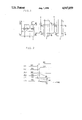
- FIG. 1 is a circuit diagram of the present invention.
- FIG. 2 is a graphic representation showing the transfer of signals within the circuit.
- FIG. 1 there is illustrated a memory cell composed of an MOS transistor M 3 and a condenser CS, and a sense amplifier 1 comprising transistors M 1 , M 2 which are driven in accordance with the status of a pair of bit lines, B/L and B/ .
- the bit line pair (B/L and B/ ) is connected to a sub-I/O line 2 via MOS transistors M 4 , M 5 , and the output nodes of the sub-I/O line are connected to the main-I/O line 3 via transistors M 6 , M 7 .
- the sub-I/O line 2 and the main-I/O line 3 each comprises, in this embodiment of the invention, two conductive lines on which complementary signals, corresponding to the signals on the bit lines B/L and B/ , are conducted.
- FIG. 2 there is represented the signal propagation in accordance with the present invention.
- the input/output lines 2 and 3 are precharged to a supply voltage V CC at the time of reading or storing information from or into a memory cell via the sense amplifier 1, as shown in FIG. 2, the status of B/L and B/ are changed in accordance with decoding signals a and b. Therefore, by the decoding signal a, the status of the sub-I/O line 2 is changed, and by the decoding signal b, the status of the main-I/O line 3 is changed so that information on the B/L and B/ lines is transferred to the I/O lines.
- the decoding signal a by the decoding signal a, the MOS transistors M 4 , M 5 are driven to transfer the signals on B/L and B/ to the sub-I/O line 2.
- the decoding signal a is provided earlier than the decoding signal b.
- information selected by an address signal is transferred to the main-I/O line 3 via the sub-I/O line 2.
- the loading components of the input/output lines are composed of a capacitance (50%) due to the Miller effect, junction capacitance (20%) and the parasitic capacitance (30%) between electrodes.
- the Miller capacitance from the input/output stage is divided into two portions, one is the capacitance loaded on the sub-I/O line and the other is that loaded on the main-I/O line.
- C J junction capacitance
- C M Miller capacitance
- C P parasitic capacitance.
- the capacitance on the I/O line is reduced, hence the speed of signal propagation is improved.
- the signal propagation delay time can be reduced by 45%.
- the I/O line divided into a sub-I/O line and a main-I/O line can reduce total capacitance, and much information can be transferred in a shorter time due to an internal buffer stage which can accommodate heavy loads promptly.
Landscapes
- Engineering & Computer Science (AREA)
- Computer Hardware Design (AREA)
- Physics & Mathematics (AREA)
- Computing Systems (AREA)
- General Engineering & Computer Science (AREA)
- Mathematical Physics (AREA)
- Dram (AREA)
Abstract
Description
Claims (3)
Applications Claiming Priority (2)
| Application Number | Priority Date | Filing Date | Title |
|---|---|---|---|
| KR88-5596[U] | 1988-05-19 | ||
| KR880005596 | 1988-05-19 |
Publications (1)
| Publication Number | Publication Date |
|---|---|
| US4947059A true US4947059A (en) | 1990-08-07 |
Family
ID=19274343
Family Applications (1)
| Application Number | Title | Priority Date | Filing Date |
|---|---|---|---|
| US07/305,278 Expired - Lifetime US4947059A (en) | 1988-05-19 | 1989-02-01 | Method of dividing an input-output line by decoding |
Country Status (1)
| Country | Link |
|---|---|
| US (1) | US4947059A (en) |
Cited By (2)
| Publication number | Priority date | Publication date | Assignee | Title |
|---|---|---|---|---|
| GB2258071B (en) * | 1991-07-23 | 1995-01-18 | Samsung Electronics Co Ltd | Data transmission circuit |
| US6107838A (en) * | 1995-02-01 | 2000-08-22 | Honeywell International, Inc. | Simultaneous two-way communication system using a single communication port |
Citations (7)
| Publication number | Priority date | Publication date | Assignee | Title |
|---|---|---|---|---|
| US4200917A (en) * | 1979-03-12 | 1980-04-29 | Motorola, Inc. | Quiet column decoder |
| US4618784A (en) * | 1985-01-28 | 1986-10-21 | International Business Machines Corporation | High-performance, high-density CMOS decoder/driver circuit |
| US4701644A (en) * | 1986-08-13 | 1987-10-20 | Harris Corporation | Low power sense amplifier |
| US4725742A (en) * | 1985-05-24 | 1988-02-16 | Hitachi, Ltd. | Semiconductor integrated circuit having a tree circuit |
| US4788457A (en) * | 1986-09-09 | 1988-11-29 | Mitsubishi Denki Kabushiki Kaisha | CMOS row decoder circuit for use in row and column addressing |
| US4803386A (en) * | 1986-11-18 | 1989-02-07 | Siemens Aktiengesellschaft | Digital amplifier configuration in integrated circuits |
| US4851716A (en) * | 1988-06-09 | 1989-07-25 | National Semiconductor Corporation | Single plane dynamic decoder |
-
1989
- 1989-02-01 US US07/305,278 patent/US4947059A/en not_active Expired - Lifetime
Patent Citations (7)
| Publication number | Priority date | Publication date | Assignee | Title |
|---|---|---|---|---|
| US4200917A (en) * | 1979-03-12 | 1980-04-29 | Motorola, Inc. | Quiet column decoder |
| US4618784A (en) * | 1985-01-28 | 1986-10-21 | International Business Machines Corporation | High-performance, high-density CMOS decoder/driver circuit |
| US4725742A (en) * | 1985-05-24 | 1988-02-16 | Hitachi, Ltd. | Semiconductor integrated circuit having a tree circuit |
| US4701644A (en) * | 1986-08-13 | 1987-10-20 | Harris Corporation | Low power sense amplifier |
| US4788457A (en) * | 1986-09-09 | 1988-11-29 | Mitsubishi Denki Kabushiki Kaisha | CMOS row decoder circuit for use in row and column addressing |
| US4803386A (en) * | 1986-11-18 | 1989-02-07 | Siemens Aktiengesellschaft | Digital amplifier configuration in integrated circuits |
| US4851716A (en) * | 1988-06-09 | 1989-07-25 | National Semiconductor Corporation | Single plane dynamic decoder |
Cited By (2)
| Publication number | Priority date | Publication date | Assignee | Title |
|---|---|---|---|---|
| GB2258071B (en) * | 1991-07-23 | 1995-01-18 | Samsung Electronics Co Ltd | Data transmission circuit |
| US6107838A (en) * | 1995-02-01 | 2000-08-22 | Honeywell International, Inc. | Simultaneous two-way communication system using a single communication port |
Similar Documents
| Publication | Publication Date | Title |
|---|---|---|
| JP2700225B2 (en) | Memory cell circuit | |
| US4435787A (en) | Semiconductor memory circuit | |
| US3983543A (en) | Random access memory read/write buffer circuits incorporating complementary field effect transistors | |
| KR940007887A (en) | Semiconductor memory device | |
| EP0251559A2 (en) | Semiconductor memory device | |
| US4107556A (en) | Sense circuit employing complementary field effect transistors | |
| JPS61239491A (en) | Electronic equipment | |
| EP0048464B1 (en) | Semiconductor memory device | |
| US5287527A (en) | Logical signal output drivers for integrated circuit interconnection | |
| US5537352A (en) | Integrated semiconductor memory configuration | |
| JPH07147090A (en) | Semiconductor memory device | |
| KR950014555B1 (en) | Semiconductor memory device with sense amplifier unit as well as data register/pointer shared between plural memory cell arrays | |
| US5982220A (en) | High speed multiplexer circuit | |
| JPH07107796B2 (en) | Non-clock static memory array | |
| US4947059A (en) | Method of dividing an input-output line by decoding | |
| EP0405411B1 (en) | Semiconductor memory having improved data readout scheme | |
| US5132930A (en) | CMOS dynamic memory device having multiple flip-flop circuits selectively coupled to form sense amplifiers specific to neighboring data bit lines | |
| US4202045A (en) | Write circuit for a read/write memory | |
| US4808857A (en) | Sense amplifier circuit for switching plural inputs at low power | |
| US4542484A (en) | Sense amplifier with high speed, stabilized read-out | |
| KR910002027B1 (en) | Method of dividing an input-output line by decoding | |
| KR940002924A (en) | Semiconductor memory | |
| KR100285031B1 (en) | Circuit arrangement for amplifying and maintaining data by supply voltage difference | |
| US5170376A (en) | Asynchronous timing circuit for a 2-coordinate memory | |
| US4831588A (en) | Integrated memory circuit having a differential read amplifier |
Legal Events
| Date | Code | Title | Description |
|---|---|---|---|
| AS | Assignment |
Owner name: SAMSUNG ELECTRONICS CO., LTD., KOREA, REPUBLIC OF Free format text: ASSIGNMENT OF ASSIGNORS INTEREST.;ASSIGNOR:KIM, CHANG-HYUN;REEL/FRAME:005037/0621 Effective date: 19890117 |
|
| STCF | Information on status: patent grant |
Free format text: PATENTED CASE |
|
| FEPP | Fee payment procedure |
Free format text: PAYOR NUMBER ASSIGNED (ORIGINAL EVENT CODE: ASPN); ENTITY STATUS OF PATENT OWNER: LARGE ENTITY |
|
| FPAY | Fee payment |
Year of fee payment: 4 |
|
| FPAY | Fee payment |
Year of fee payment: 8 |
|
| FEPP | Fee payment procedure |
Free format text: PAYER NUMBER DE-ASSIGNED (ORIGINAL EVENT CODE: RMPN); ENTITY STATUS OF PATENT OWNER: LARGE ENTITY Free format text: PAYOR NUMBER ASSIGNED (ORIGINAL EVENT CODE: ASPN); ENTITY STATUS OF PATENT OWNER: LARGE ENTITY |
|
| FPAY | Fee payment |
Year of fee payment: 12 |