EP0205488B1 - Einrichtung mit veränderlicher spalte und verfahren zu ihrer herstellung - Google Patents
Einrichtung mit veränderlicher spalte und verfahren zu ihrer herstellung Download PDFInfo
- Publication number
- EP0205488B1 EP0205488B1 EP85906110A EP85906110A EP0205488B1 EP 0205488 B1 EP0205488 B1 EP 0205488B1 EP 85906110 A EP85906110 A EP 85906110A EP 85906110 A EP85906110 A EP 85906110A EP 0205488 B1 EP0205488 B1 EP 0205488B1
- Authority
- EP
- European Patent Office
- Prior art keywords
- electrode
- substrate
- cavity
- over
- removable layer
- Prior art date
- Legal status (The legal status is an assumption and is not a legal conclusion. Google has not performed a legal analysis and makes no representation as to the accuracy of the status listed.)
- Expired - Lifetime
Links
Images
Classifications
-
- G—PHYSICS
- G02—OPTICS
- G02B—OPTICAL ELEMENTS, SYSTEMS OR APPARATUS
- G02B6/00—Light guides; Structural details of arrangements comprising light guides and other optical elements, e.g. couplings
- G02B6/24—Coupling light guides
- G02B6/26—Optical coupling means
- G02B6/35—Optical coupling means having switching means
- G02B6/351—Optical coupling means having switching means involving stationary waveguides with moving interposed optical elements
- G02B6/3512—Optical coupling means having switching means involving stationary waveguides with moving interposed optical elements the optical element being reflective, e.g. mirror
- G02B6/352—Optical coupling means having switching means involving stationary waveguides with moving interposed optical elements the optical element being reflective, e.g. mirror the reflective optical element having a shaped reflective surface, e.g. a reflective element comprising several reflective surfaces or facets that function together
-
- G—PHYSICS
- G01—MEASURING; TESTING
- G01L—MEASURING FORCE, STRESS, TORQUE, WORK, MECHANICAL POWER, MECHANICAL EFFICIENCY, OR FLUID PRESSURE
- G01L9/00—Measuring steady of quasi-steady pressure of fluid or fluent solid material by electric or magnetic pressure-sensitive elements; Transmitting or indicating the displacement of mechanical pressure-sensitive elements, used to measure the steady or quasi-steady pressure of a fluid or fluent solid material, by electric or magnetic means
- G01L9/0041—Transmitting or indicating the displacement of flexible diaphragms
- G01L9/0072—Transmitting or indicating the displacement of flexible diaphragms using variations in capacitance
-
- G—PHYSICS
- G02—OPTICS
- G02B—OPTICAL ELEMENTS, SYSTEMS OR APPARATUS
- G02B6/00—Light guides; Structural details of arrangements comprising light guides and other optical elements, e.g. couplings
- G02B6/24—Coupling light guides
- G02B6/26—Optical coupling means
- G02B6/264—Optical coupling means with optical elements between opposed fibre ends which perform a function other than beam splitting
- G02B6/266—Optical coupling means with optical elements between opposed fibre ends which perform a function other than beam splitting the optical element being an attenuator
-
- G—PHYSICS
- G09—EDUCATION; CRYPTOGRAPHY; DISPLAY; ADVERTISING; SEALS
- G09F—DISPLAYING; ADVERTISING; SIGNS; LABELS OR NAME-PLATES; SEALS
- G09F9/00—Indicating arrangements for variable information in which the information is built-up on a support by selection or combination of individual elements
- G09F9/30—Indicating arrangements for variable information in which the information is built-up on a support by selection or combination of individual elements in which the desired character or characters are formed by combining individual elements
- G09F9/37—Indicating arrangements for variable information in which the information is built-up on a support by selection or combination of individual elements in which the desired character or characters are formed by combining individual elements being movable elements
- G09F9/372—Indicating arrangements for variable information in which the information is built-up on a support by selection or combination of individual elements in which the desired character or characters are formed by combining individual elements being movable elements the positions of the elements being controlled by the application of an electric field
-
- H—ELECTRICITY
- H01—ELECTRIC ELEMENTS
- H01G—CAPACITORS; CAPACITORS, RECTIFIERS, DETECTORS, SWITCHING DEVICES, LIGHT-SENSITIVE OR TEMPERATURE-SENSITIVE DEVICES OF THE ELECTROLYTIC TYPE
- H01G5/00—Capacitors in which the capacitance is varied by mechanical means, e.g. by turning a shaft; Processes of their manufacture
- H01G5/16—Capacitors in which the capacitance is varied by mechanical means, e.g. by turning a shaft; Processes of their manufacture using variation of distance between electrodes
-
- G—PHYSICS
- G02—OPTICS
- G02B—OPTICAL ELEMENTS, SYSTEMS OR APPARATUS
- G02B6/00—Light guides; Structural details of arrangements comprising light guides and other optical elements, e.g. couplings
- G02B6/24—Coupling light guides
- G02B6/26—Optical coupling means
- G02B6/35—Optical coupling means having switching means
- G02B6/354—Switching arrangements, i.e. number of input/output ports and interconnection types
- G02B6/3544—2D constellations, i.e. with switching elements and switched beams located in a plane
- G02B6/3548—1xN switch, i.e. one input and a selectable single output of N possible outputs
- G02B6/355—1x2 switch, i.e. one input and a selectable single output of two possible outputs
-
- G—PHYSICS
- G02—OPTICS
- G02B—OPTICAL ELEMENTS, SYSTEMS OR APPARATUS
- G02B6/00—Light guides; Structural details of arrangements comprising light guides and other optical elements, e.g. couplings
- G02B6/24—Coupling light guides
- G02B6/26—Optical coupling means
- G02B6/35—Optical coupling means having switching means
- G02B6/354—Switching arrangements, i.e. number of input/output ports and interconnection types
- G02B6/3544—2D constellations, i.e. with switching elements and switched beams located in a plane
- G02B6/3548—1xN switch, i.e. one input and a selectable single output of N possible outputs
- G02B6/3552—1x1 switch, e.g. on/off switch
-
- Y—GENERAL TAGGING OF NEW TECHNOLOGICAL DEVELOPMENTS; GENERAL TAGGING OF CROSS-SECTIONAL TECHNOLOGIES SPANNING OVER SEVERAL SECTIONS OF THE IPC; TECHNICAL SUBJECTS COVERED BY FORMER USPC CROSS-REFERENCE ART COLLECTIONS [XRACs] AND DIGESTS
- Y10—TECHNICAL SUBJECTS COVERED BY FORMER USPC
- Y10T—TECHNICAL SUBJECTS COVERED BY FORMER US CLASSIFICATION
- Y10T29/00—Metal working
- Y10T29/43—Electric condenser making
- Y10T29/435—Solid dielectric type
Definitions
- This invention relates to variable gap devices and their method of manufacture.
- Variable gap devices are those which include a pair of elements and a deformable material which permits a variation in the gap between elements.
- the elements are electrodes which form a capacitor.
- the variable capacitance may be used for a wide variety of functions.
- the deformable material may take the form of a membrane which is coupled to an electrode and displaced in response to a pressure or audio input. The variation in capacitance resulting from the change in electrode gap can be detected, and the device functions as a pressure sensor or microphone, respectively.
- the membrane By applying a varying bias to the electrodes, the membrane can be caused to vibrate, and the device functions as a loudspeaker or hearing aid.
- One type of device monitors pressure by providing a single electrode mounted to the deformable element and a pair of electrodes on a substrate opposite to the single electrode with a gap therebetween. Two capacitors are therefore formed between the electrodes in the gap, and the deformation of the material is measured by the difference in capacitance of these capacitors.
- Other types of variable capacitance devices make use of a flexible reflecting electrode for controlling optical interference in order to provide a display function. (See, e.g., European Patent Application Publication No. 0035299, published September 9, 1981).
- a still further type of device employs a deformable waveguide between two electrodes such that electrostatic attraction deforms the waveguide and attenuates light propagation therethrough.
- a plurality of such devices forms an optical image recorder (see, e.g., U.S. Patent 4,162,118 issued to Conwell).
- variable capacitance device which can operate at low voltages. Further, precise sensor or display operations requires a highly uniform gap distance. The device should also be compact in order to be compatible with the microminiature nature of operations such as blood pressure sensors and the like.
- variable capacitance device as defined in claim 1.
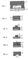
- Fig. 1 illustrates, in cross-section, a device useful for explaining the operation of, and the method of formation of, the embodiments of the invention described in Figs. 8 and 9.
- a substrate, 10 of glass included on one major surface an element, 11, which comprised chromium.
- a sheet of rubber, 12, with a small inset cavity, 13, was formed over the substrate so that the cavity overlaid the element, 11.
- the rubber was chosen to have a strong van der Waals attraction so that it would adhere to the substrate without chemically bonding thereto.
- the rubber was sold by Dow Corning under the designation Sylgard 184, but other flexible materials may be employed as long as they are compatible with the fabrication technique employed to be described. It is also desirable that any such material adhere to the substrate, but some bonding medium could be employed for this purpose if the material did not exhibit van der Waals attraction.
- the material of element, 14, in this example was aluminum and that of element, 11, was chrome, but any reflecting or conductive material could be employed, depending upon the function of the device.
- the structure When an external bias (not shown) is applied to the elements, 11 and 14, the structure operates as a variable capacitance device since the rubber material, 12, permits element, 14, to move either as a result of an attractive potential applied to the elements or as a result of some outside pressure applied to the rubber material.
- the device of Fig. 1 can be made with a stiff material instead of the rubber, 12, and a flexible membrane provided in place of substrate, 10.
- the element, 11, would move while the element, 14, would be stationary during operation. (Hereinafter, whenever it is intended to apply a bias to elements, 11 and 14, they will be described as "electrodes").
- the external bias would comprise an AC source and a resistor so as to form an RC circuit with the device of Fig. 1.
- the maximum voltage across the resistor will be determined by the resonance of the circuit which in turn is a function of the capacitance of the device.
- changes in capacitance can be detected by changes in the position of maximum voltage as known in the art.
- a DC potential could be supplied and changes in capacitance determined by measuring changes in the charge on the electrodes.
- a distributed array of such sensors could be used as a tactile sensor for a robot.
- the height of the cavity, 13, is made so small that the gap between electrodes, 11 and 14, permits operation of the device with an extremely small potential.
- the gap between electrodes was only approximately 1 pm, and the thickness of the electrodes was also approximately 1 pm.
- the width of the cavity (and electrode, 14) was approximately 1 mm, while the width of electrode, 11, was 0.9 mm. (The electrodes and cavity were square).
- the rubber, 12, was approximately 1 mm thick.
- the device may be operated at an applied AC voltage of, typically, 5-10 volts for electrostatic movement of the electrodes and be sensitive to pressures of approximately 68.95 Pascals (0.01 psi) at less than 1 volt for sensing operations where the electrodes are moved by outside mechanical forces.
- an electrode gap in the undeformed state of no greater than 10 um for electrostatic movement of the electrodes and no greater than 30 pm for mechanical movement.
- a further unique and desirable feature is the fact that the surface of the cavity including the element, 14, can be essentially flat so that the capacitance or reflectivity of the device is highly uniform across the electrodes. This is especially important when sensitive measurements are required such as in monitoring blood pressure, and when the device is used for display purposes in the manner described subsequently.
- Figs. 2-6 illustrate, in cross-section, a sequence of steps utilized to fabricate the device of Fig. 1. While a single device is shown, several devices can be batch-fabricated in accordance with the method.
- the method employs a temporary substrate, 20, which in this example was a silicon wafer but could be any substrate which is flat and generally free from imper f ec- tions.
- a glass sheet for example, could also be utilized.
- Formed over the substrate was a layer, 21, which is characterized herein as a "parting layer" since it was subsequently used to separate a portion of the device from the substrate.
- the parting layer was magnesium which was deposited by thermal evaporation to a thickness of approximately 3000 Angstroms so that the device can be separated by a galvanic coupling action. It may also be desirable to choose layers which will dissolve in a chemical or electrochemical etch to cause separation.
- the "parting layer” could comprise an entire substrate which is dissolvable in some etchant so as not to affect the remaining portion of the device.
- a removable layer 22 was formed thereon.
- the layer was a photoresist sold by Shipley Corporation under the designation AZ1450J.
- any standard photoresist or other material which can be etched or dissolved in accordance with the method can be employed.
- the thickness of this layer will determine the electrode gap. Consequently, the thickness in this example was approximately 1 pm.
- an electrode pattern was defined over the photoresist.
- the pattern could be formed, for example,by depositing through a stencil mask.
- the electrode was defined by first depositing a layer of metal, 23, in this case aluminum, over the entire substrate. The thickness of the layer was approximately 1 Ilm. The metal was then covered by a second photoresist layer, 24, which may be identical to the first photoresist layer. As illustrated in Fig. 3, the electrode was then defined by standard photolithography involving exposing the layer, 24, through a mask (not shown) and developing the resist so that it remained over the portion, 14, of the metal film, 23, which will comprise the electrode. The exposed portion of layer, 23, was then etched, for example, by a phosphoric acid based etch to define the electrode.
- the rubber material, 12, was applied over the substrate so as to encapsulate the electrode, 14, and the remaining photoresist portion, 25.
- the rubber was poured over the substrate and allowed to cure at room temperature for approximately 24 hours.
- room temperature curing is preferred since there is essentially no shrinkage of the rubber which would wrinkle the top surface of the cavity and the electrode, 14.
- higher temperature cures may be appropriate for certain applications.
- Fig. 5 The structure of Fig. 5 was then immersed in some solution which separates the rubber, 12, along with the electrode, 14, and the photoresist, 25, from the temporary substrate, 20, along the parting layer, 21.
- separation was accomplished by galvanic coupling. That is, when two dissimilar metals in electrical contact are placed in a bath where electrons are available, the metal which give up ions will corrode while the metal which gives up electrons remains essentially unchanged.
- the magnesium layer, 21, acted as the corroding metal and the substrate, 20, acted as the noncorroding metal when the structure was immersed in a bath of HCI.
- the rubber parted from the substrate, typically, in approximately 30 minutes.
- any remaining photoresist portion, 25, was removed subsequently from under the electrode, 14, for example, by rinsing in acetone followed by isopropyl alcohol. This leaves the structure shown in Fig. 6 where the cavity, 13, with electrode, 14, on the top surface was formed in the rubber material. If desired, the portion, 25, could be removed at the same time as the parting of the rubber from the substrate by including in the bath a material which also dissolves the layer, 25.
- the electrode, 11, (see Fig. 1) was formed on the permanent substrate, 10, by chrome thermal evaporation followed by standard photolithography.
- the cavity from the structure of Fig. 6 was then aligned with the substrate electrode and the rubber made to contact the substrate surface. Since the rubber adheres well to most surfaces by van der Waals attraction, only slight pressure is needed to cause the rubber to adhere to the substrate.
- the rubber material may be sealed to the substrate by a number of techniques. In this example, the sealing was accomplished by including a wire (not shown) on the substrate around the periphery of the cavity and sending current through the wire to resistively heat the rubber.
- the device of Fig. 1 can be utilized, for example, as a pressure sensor by providing leads to the top and bottom electrodes, 14 and 11, during the electrode definition step (Fig. 3) and applying an external AC or DC bias. Any change in capacitance as a result of moving electrode, 14, due to pressure can be detected as previously described.
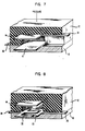
- Fig. 7 which shows the rubber, 12, partially cut away, the lead, 30, to the bottom electrode could be formed on the substrate, 10, and the lead, 31, to the top electrode can be formed along the top surface of the cavity.
- the leads may be formed orthogonally if desired.
- the same device could be used as a pressure switch which is turned on only when the two electrodes, 11 and 14, make contact.
- An array of devices such as shown Fig. 7 formed in the same rubber material, 12, can be utilized as a touch screen as long as the rubber and electrodes are transparent or they obscure only a small fraction of the viewing area.
- all leads are provided on the surface of the substrate, as shown in Fig. 8.
- the bottom electrode of Fig. 7 is replaced by two interdigitated electrodes, 32 and 33, each with a lead, 34 and 35, formed on the substrate.
- Each lead electrically connects its corresponding electrode to a bias (not shown).
- the two electrodes, 32 and 33 are therefore capacitively coupled through the top electrode and can sense the position of the top electrode without any leads applied thereto. Further, the device may be operated even if cracks develop in the top electrode since the AC capacitance would not be affected.
- This embodiment can be operated as speakers or microphones with the appropriate potential applied to the electrodes. Further, such an embodiment could be employed in the segments of a display.
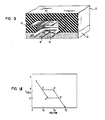
- FIG. 9 illustrates a high impedance switch.
- Both top and bottom electrodes each comprise a U-shaped portion, 40 and 42, and interdigitated therewith are electrically isolated switch contact portion, 41 and 43. (Leads coupled to these electrodes are not shown in this figure for the sake of simplicity).
- An attractive potential applied between U-shaped portions, 40 and 42 pulls down the top electrode allowing the switch contacts, 41 and 43, which are electrically isolated from the U-shaped portions, to come in contact and close whatever circuit is coupled to these contacts.
- an electrostatic relay with high electrical isolation and requiring low power can be produced.
- a high impedance switch for example as shown in Fig. 9, can be incorporated into a display segment if it is desirable to have the segment remain on after the voltage is removed. That is, the high impedance when the switch is opened causes the capacitor to remain charged for a period of time after the bias to the segment is removed, thus providing a latching phenomenon.
- Fig. 8 It is also possible to incorporate the embodiment of Fig. 8 into a display which, at a particular voltage, has two stable modes, thereby eliminating the requirement of a separate switch for each segment if latching is desired.
- a display can therefore be made to operate according to the hysteresis plot of Fig. 10.
- X o is the displacement of the electrodes in the undeformed state.
- a voltage of V>V' would be applied to cause an electrode separation of X ⁇ X c .
- One example of a structure which can be operated in such a manner is when one of the electrodes, say the top electrode, is broken into portions and interspersed between the portions are stubs formed from the rubber material, 12. Initially, the displacement of the rubber, 12, as a function of pressure will be linear according to Hooke's Law. Once the stubs make contact with the lower electrode portions the pressure versus displacement curve will experience a sharp change in slope due to the resistance provided by the stubs against further displacement.
Landscapes
- Physics & Mathematics (AREA)
- General Physics & Mathematics (AREA)
- Engineering & Computer Science (AREA)
- Optics & Photonics (AREA)
- Power Engineering (AREA)
- Theoretical Computer Science (AREA)
- Microelectronics & Electronic Packaging (AREA)
- Mechanical Light Control Or Optical Switches (AREA)
- Measuring Fluid Pressure (AREA)
Claims (17)
Applications Claiming Priority (4)
| Application Number | Priority Date | Filing Date | Title |
|---|---|---|---|
| US68719284A | 1984-12-28 | 1984-12-28 | |
| US687192 | 1984-12-28 | ||
| US06/744,382 US4617608A (en) | 1984-12-28 | 1985-06-13 | Variable gap device and method of manufacture |
| US744382 | 1985-06-13 |
Publications (2)
| Publication Number | Publication Date |
|---|---|
| EP0205488A1 EP0205488A1 (de) | 1986-12-30 |
| EP0205488B1 true EP0205488B1 (de) | 1990-05-30 |
Family
ID=27103957
Family Applications (1)
| Application Number | Title | Priority Date | Filing Date |
|---|---|---|---|
| EP85906110A Expired - Lifetime EP0205488B1 (de) | 1984-12-28 | 1985-11-15 | Einrichtung mit veränderlicher spalte und verfahren zu ihrer herstellung |
Country Status (4)
| Country | Link |
|---|---|
| US (1) | US4617608A (de) |
| EP (1) | EP0205488B1 (de) |
| DE (1) | DE3578019D1 (de) |
| WO (1) | WO1986004182A1 (de) |
Families Citing this family (62)
| Publication number | Priority date | Publication date | Assignee | Title |
|---|---|---|---|---|
| US4945230A (en) * | 1984-07-06 | 1990-07-31 | Metricor, Inc. | Optical measuring device using a spectral modulation sensor having an optically resonant structure |
| US4689246A (en) * | 1984-10-26 | 1987-08-25 | Itek Corporation | Method of fabricating a PbS-PbSe IR detector array |
| US5039491A (en) * | 1989-01-27 | 1991-08-13 | Metricor, Inc. | Optical oxygen sensor |
| US5039492A (en) * | 1989-01-27 | 1991-08-13 | Metricor, Inc. | Optical pH and gas concentration sensor |
| US5021731A (en) * | 1989-02-21 | 1991-06-04 | Metricor, Inc. | Thermo-optical current sensor and thermo-optical current sensing systems |
| US4983824A (en) * | 1989-07-06 | 1991-01-08 | Metricor Inc. | Optically resonant sensor with increased monotonic range |
| EP0436454A1 (de) * | 1990-01-05 | 1991-07-10 | Agrotique Sarl | Detektor für zu säendes Korn |
| US5280173A (en) * | 1992-01-31 | 1994-01-18 | Brown University Research Foundation | Electric and electromagnetic field sensing system including an optical transducer |
| US5526172A (en) * | 1993-07-27 | 1996-06-11 | Texas Instruments Incorporated | Microminiature, monolithic, variable electrical signal processor and apparatus including same |
| US7550794B2 (en) | 2002-09-20 | 2009-06-23 | Idc, Llc | Micromechanical systems device comprising a displaceable electrode and a charge-trapping layer |
| US7297471B1 (en) | 2003-04-15 | 2007-11-20 | Idc, Llc | Method for manufacturing an array of interferometric modulators |
| US5636052A (en) * | 1994-07-29 | 1997-06-03 | Lucent Technologies Inc. | Direct view display based on a micromechanical modulation |
| US6377383B1 (en) | 1997-09-04 | 2002-04-23 | The University Of British Columbia | Optical switching by controllable frustration of total internal reflection |
| US7140102B2 (en) * | 2001-09-02 | 2006-11-28 | Borealis Technical Limited | Electrode sandwich separation |
| FR2824643B1 (fr) * | 2001-05-10 | 2003-10-31 | Jean Pierre Lazzari | Dispositif de modulation de lumiere |
| US20080061114A1 (en) * | 2001-09-02 | 2008-03-13 | Zara Taliashvili | Method for the fabrication of low temperature vacuum sealed bonds using diffusion welding |
| US6452734B1 (en) | 2001-11-30 | 2002-09-17 | The University Of British Columbia | Composite electrophoretically-switchable retro-reflective image display |
| US6794119B2 (en) | 2002-02-12 | 2004-09-21 | Iridigm Display Corporation | Method for fabricating a structure for a microelectromechanical systems (MEMS) device |
| ATE516879T1 (de) * | 2002-02-12 | 2011-08-15 | Cellectricon Ab | Systeme und verfahren zur schnellen änderung der lösungsumgebung von sensoren |
| US6891658B2 (en) | 2002-03-04 | 2005-05-10 | The University Of British Columbia | Wide viewing angle reflective display |
| US6865011B2 (en) * | 2002-07-30 | 2005-03-08 | The University Of British Columbia | Self-stabilized electrophoretically frustrated total internal reflection display |
| US7781850B2 (en) | 2002-09-20 | 2010-08-24 | Qualcomm Mems Technologies, Inc. | Controlling electromechanical behavior of structures within a microelectromechanical systems device |
| AU2003278461A1 (en) | 2002-10-16 | 2004-05-04 | Cellectricon Ab | Nanoelectrodes and nanotips for recording transmembrane currents in a plurality of cells |
| TW567355B (en) * | 2003-04-21 | 2003-12-21 | Prime View Int Co Ltd | An interference display cell and fabrication method thereof |
| DE10321099A1 (de) * | 2003-05-09 | 2004-11-25 | Cgs Sensortechnik Gmbh | Vorrichtung zur Druckmessung |
| TW570896B (en) * | 2003-05-26 | 2004-01-11 | Prime View Int Co Ltd | A method for fabricating an interference display cell |
| US7221495B2 (en) * | 2003-06-24 | 2007-05-22 | Idc Llc | Thin film precursor stack for MEMS manufacturing |
| TWI231865B (en) | 2003-08-26 | 2005-05-01 | Prime View Int Co Ltd | An interference display cell and fabrication method thereof |
| TW593126B (en) * | 2003-09-30 | 2004-06-21 | Prime View Int Co Ltd | A structure of a micro electro mechanical system and manufacturing the same |
| US7684104B2 (en) | 2004-09-27 | 2010-03-23 | Idc, Llc | MEMS using filler material and method |
| US7405861B2 (en) | 2004-09-27 | 2008-07-29 | Idc, Llc | Method and device for protecting interferometric modulators from electrostatic discharge |
| US7373026B2 (en) | 2004-09-27 | 2008-05-13 | Idc, Llc | MEMS device fabricated on a pre-patterned substrate |
| US7492502B2 (en) | 2004-09-27 | 2009-02-17 | Idc, Llc | Method of fabricating a free-standing microstructure |
| US7161730B2 (en) * | 2004-09-27 | 2007-01-09 | Idc, Llc | System and method for providing thermal compensation for an interferometric modulator display |
| US7349136B2 (en) | 2004-09-27 | 2008-03-25 | Idc, Llc | Method and device for a display having transparent components integrated therein |
| US7369296B2 (en) | 2004-09-27 | 2008-05-06 | Idc, Llc | Device and method for modifying actuation voltage thresholds of a deformable membrane in an interferometric modulator |
| US7417783B2 (en) | 2004-09-27 | 2008-08-26 | Idc, Llc | Mirror and mirror layer for optical modulator and method |
| US7553684B2 (en) | 2004-09-27 | 2009-06-30 | Idc, Llc | Method of fabricating interferometric devices using lift-off processing techniques |
| US7429334B2 (en) | 2004-09-27 | 2008-09-30 | Idc, Llc | Methods of fabricating interferometric modulators by selectively removing a material |
| TW200628877A (en) | 2005-02-04 | 2006-08-16 | Prime View Int Co Ltd | Method of manufacturing optical interference type color display |
| US7164536B2 (en) * | 2005-03-16 | 2007-01-16 | The University Of British Columbia | Optically coupled toroidal lens:hemi-bead brightness enhancer for total internal reflection modulated image displays |
| WO2006129821A1 (ja) * | 2005-05-31 | 2006-12-07 | Ngk Insulators, Ltd. | 物体の通過検出装置 |
| WO2007013939A1 (en) | 2005-07-22 | 2007-02-01 | Qualcomm Incorporated | Support structure for mems device and methods therefor |
| US7630114B2 (en) | 2005-10-28 | 2009-12-08 | Idc, Llc | Diffusion barrier layer for MEMS devices |
| US7795061B2 (en) | 2005-12-29 | 2010-09-14 | Qualcomm Mems Technologies, Inc. | Method of creating MEMS device cavities by a non-etching process |
| US7382515B2 (en) | 2006-01-18 | 2008-06-03 | Qualcomm Mems Technologies, Inc. | Silicon-rich silicon nitrides as etch stops in MEMS manufacture |
| US7547568B2 (en) | 2006-02-22 | 2009-06-16 | Qualcomm Mems Technologies, Inc. | Electrical conditioning of MEMS device and insulating layer thereof |
| US7450295B2 (en) | 2006-03-02 | 2008-11-11 | Qualcomm Mems Technologies, Inc. | Methods for producing MEMS with protective coatings using multi-component sacrificial layers |
| US7643203B2 (en) * | 2006-04-10 | 2010-01-05 | Qualcomm Mems Technologies, Inc. | Interferometric optical display system with broadband characteristics |
| US7711239B2 (en) | 2006-04-19 | 2010-05-04 | Qualcomm Mems Technologies, Inc. | Microelectromechanical device and method utilizing nanoparticles |
| US7417784B2 (en) | 2006-04-19 | 2008-08-26 | Qualcomm Mems Technologies, Inc. | Microelectromechanical device and method utilizing a porous surface |
| US7623287B2 (en) | 2006-04-19 | 2009-11-24 | Qualcomm Mems Technologies, Inc. | Non-planar surface structures and process for microelectromechanical systems |
| US7527996B2 (en) | 2006-04-19 | 2009-05-05 | Qualcomm Mems Technologies, Inc. | Non-planar surface structures and process for microelectromechanical systems |
| US7369292B2 (en) | 2006-05-03 | 2008-05-06 | Qualcomm Mems Technologies, Inc. | Electrode and interconnect materials for MEMS devices |
| US7321457B2 (en) * | 2006-06-01 | 2008-01-22 | Qualcomm Incorporated | Process and structure for fabrication of MEMS device having isolated edge posts |
| US7405863B2 (en) | 2006-06-01 | 2008-07-29 | Qualcomm Mems Technologies, Inc. | Patterning of mechanical layer in MEMS to reduce stresses at supports |
| US7566664B2 (en) | 2006-08-02 | 2009-07-28 | Qualcomm Mems Technologies, Inc. | Selective etching of MEMS using gaseous halides and reactive co-etchants |
| US7763546B2 (en) | 2006-08-02 | 2010-07-27 | Qualcomm Mems Technologies, Inc. | Methods for reducing surface charges during the manufacture of microelectromechanical systems devices |
| KR20090125087A (ko) | 2007-02-20 | 2009-12-03 | 퀄컴 엠이엠스 테크놀로지스, 인크. | 마이크로전자기계 시스템〔mems〕의 에칭장치 및 에칭 방법 |
| US7719752B2 (en) | 2007-05-11 | 2010-05-18 | Qualcomm Mems Technologies, Inc. | MEMS structures, methods of fabricating MEMS components on separate substrates and assembly of same |
| KR20100061731A (ko) * | 2007-09-14 | 2010-06-08 | 퀄컴 엠이엠스 테크놀로지스, 인크. | Mems 제조에 이용되는 에칭 방법 |
| JP6850686B2 (ja) * | 2017-06-12 | 2021-03-31 | 日本電信電話株式会社 | 圧力センサおよび中空光導波路の製造方法 |
Family Cites Families (16)
| Publication number | Priority date | Publication date | Assignee | Title |
|---|---|---|---|---|
| US2576489A (en) * | 1950-01-20 | 1951-11-27 | Tinius Olsen Testing Mach Co | Capacitance strain gauge |
| US2868894A (en) * | 1955-09-14 | 1959-01-13 | Theodore J Schultz | Miniature condenser microphone |
| US3426209A (en) * | 1967-09-11 | 1969-02-04 | Texas Instruments Inc | Light responsive variable capacitor |
| DE1938181A1 (de) * | 1968-08-01 | 1970-06-04 | South African Inv S Dev Corp | Vorrichtung zur Bestimmung von Lasten |
| GB1450709A (en) * | 1973-12-31 | 1976-09-29 | Birchall D J | Pressure transducers |
| US4065649A (en) * | 1975-06-30 | 1977-12-27 | Lake Center Industries | Pressure sensitive matrix switch having apertured spacer with flexible double sided adhesive intermediate and channels optionally interposed between apertures |
| US4017495A (en) * | 1975-10-23 | 1977-04-12 | Bell Telephone Laboratories, Incorporated | Encapsulation of integrated circuits |
| US4203128A (en) * | 1976-11-08 | 1980-05-13 | Wisconsin Alumni Research Foundation | Electrostatically deformable thin silicon membranes |
| AU501488B1 (en) * | 1977-06-06 | 1979-06-21 | Matsushita Electric Industrial Co., Ltd. | Humidity sensor |
| US4151578A (en) * | 1977-08-01 | 1979-04-24 | Kavlico Corporation | Capacitive pressure transducer |
| JPS54101176A (en) * | 1978-01-26 | 1979-08-09 | Shinetsu Polymer Co | Contact member for push switch |
| US4158310A (en) * | 1978-01-30 | 1979-06-19 | University Of Southern California | Optical pressure transducer of randomly distributed fiber optics |
| GB2064873B (en) * | 1979-11-26 | 1984-09-05 | Eventoff Franklin Neal | Pressure sensitive electric switch |
| NL8001281A (nl) * | 1980-03-04 | 1981-10-01 | Philips Nv | Weergeefinrichting. |
| US4368645A (en) * | 1980-09-26 | 1983-01-18 | United Technologies Corporation | Optical pressure sensor |
| US4530029A (en) * | 1984-03-12 | 1985-07-16 | United Technologies Corporation | Capacitive pressure sensor with low parasitic capacitance |
-
1985
- 1985-06-13 US US06/744,382 patent/US4617608A/en not_active Ceased
- 1985-11-15 WO PCT/US1985/002264 patent/WO1986004182A1/en not_active Ceased
- 1985-11-15 DE DE8585906110T patent/DE3578019D1/de not_active Expired - Lifetime
- 1985-11-15 EP EP85906110A patent/EP0205488B1/de not_active Expired - Lifetime
Non-Patent Citations (1)
| Title |
|---|
| Report 166 0f Advisor Group for Aeronautical Research and Develpment, March 1968 J. Dimeff:"A survey of new developments in pressure measuring techniques in the NACA" * |
Also Published As
| Publication number | Publication date |
|---|---|
| US4617608A (en) | 1986-10-14 |
| WO1986004182A1 (en) | 1986-07-17 |
| EP0205488A1 (de) | 1986-12-30 |
| DE3578019D1 (de) | 1990-07-05 |
Similar Documents
| Publication | Publication Date | Title |
|---|---|---|
| US4617608A (en) | Variable gap device and method of manufacture | |
| EP0631122B1 (de) | Miniaturdruckwandler hoher Empfindlichkeit mit gespannter Membran | |
| US5447068A (en) | Digital capacitive accelerometer | |
| Zavracky et al. | Micromechanical switches fabricated using nickel surface micromachining | |
| EP0619471B1 (de) | Verfahren zur Herstellung eines Bewegungsmessaufnehmers | |
| US20030048036A1 (en) | MEMS comb-finger actuator | |
| US7992271B2 (en) | Process of manufacturing a piezoelectric actuator for tunable electronic components on a carrier substrate | |
| US5658698A (en) | Microstructure, process for manufacturing thereof and devices incorporating the same | |
| EP0136249B1 (de) | Silizium-Glas-Silizium kapazitiver Druckwandler mit drei Elektroden | |
| US5620933A (en) | Micromachined relay and method of forming the relay | |
| EP1187789B1 (de) | Verfahren zur herstellung von genauen mikroelektromechanischen strukturen, und so hergestellte mikrostrukturen | |
| US6388299B1 (en) | Sensor assembly and method | |
| EP0156757A2 (de) | Kapazitiver Druckmessfühler mit niedriger parasitärer Kapazität | |
| US20120025333A1 (en) | Mems element and method for manufacturing same | |
| USRE33651E (en) | Variable gap device and method of manufacture | |
| Sprenkels et al. | Development of an electret microphone in silicon | |
| JPH10142254A (ja) | 半導体集積型容量加速度センサおよびその製法 | |
| JPH04143628A (ja) | 静電容量式圧力センサ | |
| CA2185532C (en) | Electrode structure and method for anodically-bonded capacitive sensors | |
| US7268653B2 (en) | Microelectromechanical system able to switch between two stable positions | |
| Linder et al. | Investigations on free-standing polysilicon beams in view of their application as transducers | |
| US5763782A (en) | Micromechanical sensor | |
| US3868719A (en) | Thin ribbon-like glass backed transducers | |
| Sasayama et al. | Highly reliable silicon micromachined physical sensors in mass production | |
| US5744725A (en) | Capacitive pressure sensor and method of fabricating same |
Legal Events
| Date | Code | Title | Description |
|---|---|---|---|
| PUAI | Public reference made under article 153(3) epc to a published international application that has entered the european phase |
Free format text: ORIGINAL CODE: 0009012 |
|
| AK | Designated contracting states |
Kind code of ref document: A1 Designated state(s): BE DE FR GB IT |
|
| 17P | Request for examination filed |
Effective date: 19861222 |
|
| 17Q | First examination report despatched |
Effective date: 19880728 |
|
| GRAA | (expected) grant |
Free format text: ORIGINAL CODE: 0009210 |
|
| AK | Designated contracting states |
Kind code of ref document: B1 Designated state(s): BE DE FR GB IT |
|
| PG25 | Lapsed in a contracting state [announced via postgrant information from national office to epo] |
Ref country code: IT Free format text: LAPSE BECAUSE OF FAILURE TO SUBMIT A TRANSLATION OF THE DESCRIPTION OR TO PAY THE FEE WITHIN THE PRESCRIBED TIME-LIMIT;WARNING: LAPSES OF ITALIAN PATENTS WITH EFFECTIVE DATE BEFORE 2007 MAY HAVE OCCURRED AT ANY TIME BEFORE 2007. THE CORRECT EFFECTIVE DATE MAY BE DIFFERENT FROM THE ONE RECORDED. Effective date: 19900530 Ref country code: BE Effective date: 19900530 Ref country code: FR Effective date: 19900530 |
|
| REF | Corresponds to: |
Ref document number: 3578019 Country of ref document: DE Date of ref document: 19900705 |
|
| EN | Fr: translation not filed | ||
| PLBE | No opposition filed within time limit |
Free format text: ORIGINAL CODE: 0009261 |
|
| STAA | Information on the status of an ep patent application or granted ep patent |
Free format text: STATUS: NO OPPOSITION FILED WITHIN TIME LIMIT |
|
| 26N | No opposition filed | ||
| PGFP | Annual fee paid to national office [announced via postgrant information from national office to epo] |
Ref country code: GB Payment date: 20011116 Year of fee payment: 17 |
|
| PGFP | Annual fee paid to national office [announced via postgrant information from national office to epo] |
Ref country code: DE Payment date: 20011230 Year of fee payment: 17 |
|
| REG | Reference to a national code |
Ref country code: GB Ref legal event code: IF02 |
|
| PG25 | Lapsed in a contracting state [announced via postgrant information from national office to epo] |
Ref country code: GB Free format text: LAPSE BECAUSE OF NON-PAYMENT OF DUE FEES Effective date: 20021115 |
|
| PG25 | Lapsed in a contracting state [announced via postgrant information from national office to epo] |
Ref country code: DE Free format text: LAPSE BECAUSE OF NON-PAYMENT OF DUE FEES Effective date: 20030603 |
|
| GBPC | Gb: european patent ceased through non-payment of renewal fee |