EP0205235A2 - Verfahren und Vorrichtung für Flüssigkristallaufzeichnung von Analogindikatoren - Google Patents
Verfahren und Vorrichtung für Flüssigkristallaufzeichnung von Analogindikatoren Download PDFInfo
- Publication number
- EP0205235A2 EP0205235A2 EP86302570A EP86302570A EP0205235A2 EP 0205235 A2 EP0205235 A2 EP 0205235A2 EP 86302570 A EP86302570 A EP 86302570A EP 86302570 A EP86302570 A EP 86302570A EP 0205235 A2 EP0205235 A2 EP 0205235A2
- Authority
- EP
- European Patent Office
- Prior art keywords
- gap
- liquid crystal
- input signal
- electric field
- voltage
- Prior art date
- Legal status (The legal status is an assumption and is not a legal conclusion. Google has not performed a legal analysis and makes no representation as to the accuracy of the status listed.)
- Withdrawn
Links
- 239000004973 liquid crystal related substance Substances 0.000 title claims abstract description 116
- 238000000034 method Methods 0.000 title claims description 11
- 239000000463 material Substances 0.000 claims abstract description 81
- 230000005684 electric field Effects 0.000 claims abstract description 46
- 230000003287 optical effect Effects 0.000 claims abstract description 33
- 230000001143 conditioned effect Effects 0.000 claims description 3
- 230000003750 conditioning effect Effects 0.000 claims 1
- 239000004988 Nematic liquid crystal Substances 0.000 description 6
- 239000000446 fuel Substances 0.000 description 4
- 239000007788 liquid Substances 0.000 description 4
- 230000005540 biological transmission Effects 0.000 description 3
- 239000013078 crystal Substances 0.000 description 3
- 230000005669 field effect Effects 0.000 description 3
- WYTGDNHDOZPMIW-RCBQFDQVSA-N alstonine Natural products C1=CC2=C3C=CC=CC3=NC2=C2N1C[C@H]1[C@H](C)OC=C(C(=O)OC)[C@H]1C2 WYTGDNHDOZPMIW-RCBQFDQVSA-N 0.000 description 2
- 238000007789 sealing Methods 0.000 description 2
- 239000004986 Cholesteric liquid crystals (ChLC) Substances 0.000 description 1
- 239000011358 absorbing material Substances 0.000 description 1
- 238000000149 argon plasma sintering Methods 0.000 description 1
- 230000002238 attenuated effect Effects 0.000 description 1
- 239000004020 conductor Substances 0.000 description 1
- 238000010276 construction Methods 0.000 description 1
- 238000005520 cutting process Methods 0.000 description 1
- 239000012769 display material Substances 0.000 description 1
- 238000009826 distribution Methods 0.000 description 1
- 238000004070 electrodeposition Methods 0.000 description 1
- 239000011521 glass Substances 0.000 description 1
- 230000001939 inductive effect Effects 0.000 description 1
- 230000031700 light absorption Effects 0.000 description 1
- 239000011344 liquid material Substances 0.000 description 1
- 238000004519 manufacturing process Methods 0.000 description 1
- 239000000203 mixture Substances 0.000 description 1
- 230000002093 peripheral effect Effects 0.000 description 1
- XOLBLPGZBRYERU-UHFFFAOYSA-N tin dioxide Chemical compound O=[Sn]=O XOLBLPGZBRYERU-UHFFFAOYSA-N 0.000 description 1
- 229910001887 tin oxide Inorganic materials 0.000 description 1
Images


Classifications
-
- G—PHYSICS
- G01—MEASURING; TESTING
- G01D—MEASURING NOT SPECIALLY ADAPTED FOR A SPECIFIC VARIABLE; ARRANGEMENTS FOR MEASURING TWO OR MORE VARIABLES NOT COVERED IN A SINGLE OTHER SUBCLASS; TARIFF METERING APPARATUS; MEASURING OR TESTING NOT OTHERWISE PROVIDED FOR
- G01D7/00—Indicating measured values
Definitions
- the invention relates to devices for presenting analog displays of electrical input signals which are a function of a variable to be displayed.
- the variable can include electrical variables such as voltage, current, resistance, etc.
- the variables may be those representative of physical conditions such as temperature, pressure, velocity, liquid level and the like.
- the invention further relates to the use of liquid crystal displays as analog indicators or, in particular, as analog bar graph indicators.
- the invention utilizes liquid crystal materials in which the propagation or characteristics of light incident thereon can be altered by inducing an electric or magnetic field in the liquid crystal material.
- liquid crystal materials include, but are not limited to, nematic liquid crystal materials possessing dynamic or quiescent scattering, or twisted field-effect electro-optical properties, and the mixtures of these nematic liquid crystal materials with cholesteric liquid crystal materials.
- a dynamic scattering transmissive liquid crystal material In a dynamic scattering transmissive liquid crystal material, light is transmitted substantially unaffected through the material in the absence of an electric field across the liquid material. When an electric field of sufficient magnitude is induced in the liquid crystal material, light incident upon the material is optically scattered and transmission of light through the-n ⁇ aterial is substantially prevented:
- a quiescent scattering transmissive liquid crystal material in the absence of an electric field, scatters incident light, while an electric field induced in the quiescent liquid crystal material causes it to transmit incident light therethrough.
- a twisted nematic liquid crystal material layers of molecules at opposed surfaces of the material can be caused to be aligned at an angle with each other in the absence of a field.
- the molecules between the opposed surfaces have varying alignments with the result that the molecular orientation through the material from one surface to the other is helically "twisted".
- linearly polarized light when entering a twisted nematic liquid crystal display, parallel to the optical axis on one side of the display, is rotated by the angle formed by the opposed surface molecules, e.g., 90°, as the light passes through the liquid crystal material. The light then emerges at the other side of the display still linearly polarized.
- the display appears transparent.
- the application of an electric field to the liquid crystal material above the threshold tilts the director axes parallel to the field. This eliminates the twisted alignment of the molecules with the result that the display appears opaque or dark.
- the electric field converts the display device from the twisted transparent off-state to a uniaxial nematic, dark on-state when viewed between properly oriented cross polarizers.
- liquid crystal display elements which present information relating to variables such as those of electrical or physical conditions have typically been in connection with the presentation of data in an alphanumeric format.
- the variables typically displayed on liquid crystal displays are displayed as digital data.
- analog presentations of conditions such as needle or pointer presentations have been traditionally used.
- needle or pointer presentations have given way to analog bar graph presentations in which the extent or position of a movable bar with respect to fixed indicia provides the analog information.
- Analog bar graphs have the advantage of needle or pointer presentations in enabling the user to extract valuable and accurate information at a glance.
- Analog bar graph presentations also have the advantage of enabling a normal, standard, or nominal condition of the bar graph of each of a plurality of presentations disposed adjacent to one another to be placed adjacent a common reference line or location. This arrangement accentuates the departure of any bar graph of the plurality from the normal condition.
- microprocessors also have been used to drive the individual conductive strips or lines of a liquid crystal display element in response to an electrical input signal.
- An object of the invention is to provide an analog display device using a liquid crystal display . element without the need of driving the various line or strip electrodes of the array of the liquid crystal display element.
- Another object of the invention is to provide an optical presentation of the magnitude of an electrical input signal by means of a liquid crystal display element to which only the electrical input signal is connected.
- a further object of the invention is to provide a bar graph presentation of the magnitude of an electrical input signal by means of a liquid crystal display element in which the input signal is applied both across the load electrode of the liquid crystal display element and to the address electrode of the liquid crystal display element.
- Still a further object of the invention is to provide an analog bar graph presentation of a voltage by means of a liquid crystal display element.
- It is also an object of the invention is to provide flag or annunciator displays and alphanumeric legends alone by means of a liquid crystal display element or in combination with an analog bar graph presentation.
- liquid crystal materials in displays of analog indicators as opposed to conventional electrical displays has the advantages of providing very low power consumption and voltage threshold, of long life, of reduced size, of a wide viewing angle in the reflecting mode, and of avoiding image washout at high ambient light levels.
- the device of the invention includes liquid crystal material disposed in a gap formed between a pair of spaced plates with an address electrode on one plate and a load electrode on the other plate.
- the inner surface of the address electrode plate is covered with a substantially conductive material forming an address electrode.
- the inner surface of the load electrode plate is covered with an array of closely spaced conductive strips or lines, electrically connected to one by another means of a resistive material.
- a sensor i.e. a transducer
- the resistive material connecting the conductive lines of the load electrode creates a predetermined voltage gradient across the array of conductive lines as determined by the resistance characteristic of the resistive material along its length. Accordingly each line of the load electrode has a different voltage when a voltage is applied to one input terminal of the resistive material and the other end is grounded.
- the address electrode is adapted to be maintained at a voltage equal to the voltage applied to the input terminal of the resistive material.
- the liquid crystal material in the region of such lines scatters light, if, for example, a quiescent scattering transmissive liquid crystal material is used.
- the potantial difference between the address and load plates will be approaching maximum and will approximately equal the voltage being applied to the address electrode-and the toad electrode.
- Quiescent scattering transmissive liquid crystal material in this region will allow light to pass through.
- the maximum potential difference between the address and load electrodes near the grounded terminal of the resistive material will change.
- the higher the input voltage the higher the voltage along the conductive lines on the load electrode and the steeper the gradient.
- the point at which the potential difference between the address and load electrodes will begin to cause quiescent scattering transmissive liquid crystal to transmit light will move closer and closer toward the input terminal of the resistor.
- the potential difference between the address and load electrodes becomes smaller, and the quiescent scattering liquid crystal will only transmit light near the grounded terminal of the resistive material.
- the conductive lines can be placed in a variety of configurations.
- the lines can be horizontal and parallel to form a bar graph display or radially arranged triangles to simulate a needle indicator.
- the potential across the electrodes will change and the areas of the display which are dark or bright will change in size.
- liquid crystal materials can be used in accordance with the invention including transmissive, transflexive, reflective quiescent scattering, dynamic scattering, and field effect liquid crystal materials.
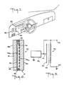
- Display device 30 includes a liquid crystal display element 31 having a pair of plates 32 and 34 with gap 33 therebetween.
- Address electrode plate 32 is maintained in closely spaced relation to a load electrode plate 34 by means of a peripheral sealing member 36.
- Gap 33 between the plates contains liquid crystal display material 38.
- the construction of a liquid crystal display element suitable to be used in the display device of the invention is shown in the applicant's U.S. Patent No. 3,820,875, which issued on June 28, 1974.
- the disclosure of the '875 patent is incorporated herein by reference.
- the disclosure of applicant's U.S. Patent No. 4,493,531 is also incorporated herein by reference.
- the address electrode 40 is in the form of a sheet disposed on inner surface 32a of plate 32 and extending over an area in which it is desired to vary the optical appearance of the display.
- display element 31 may include an address electrode 40 of rectangular shape for use in creating an analog bar graph representation.
- the address electrode 40 is provided with an electrical connection 41 to a source 42 of an electrical input signal as shown in FIG. 3.
- Electrode 40 shown in FIGS. 2 and 3 is substantially non-resistive. As a result, a voltage applied at any point to electrode 40 is present as substantially the same voltage over the entire area of electrode 40.
- an impedance element such as resistor 50 having input terminal 52 and grounded terminal 54.
- Resistor 50 defines a resistive electrical path of predetermined length and configuration between the terminals 52 and 54.
- a positive voltage of + 10 volts can be applied to input terminal 52 from source 42 which is electrically connected both to input terminal 52 and to the address electrode 40.
- Resistor 50 is connected to an array of closely spaced substantially parallel conductive strips or load lines 60 - (FIGS. 2, 3 and 5).
- Resistor 50 is conditioned to be either substantially electrically linear or non-linear along its length as determined, for example, by the characteristic of the input signal to be indicated and the type of scale to be displayed.
- resistor 50 can be printed in a tapered form to provide an audio taper characteristic, a logarithmic characteristic, or a power or exponential characteristic. Any of these characteristics can be combined with one another or with linear resistors to obtain the desired characteristic of the bar presentation, i.e., linear or non-linear with respect to the input signal.
- conductive strips 60 which extend substantially horizontally are adapted to form a vertical bar graph analog presentation.
- conductive strips 60 which extend substantially vertically are adapted to form a horizontal bar graph analog presentation.
- address electrode 50 and load lines 60 are located on spaced-apart parallel planes defined by the inner surface 32a of address plate 32 and inner surface 34a of load plate 34. It is preferable for the intervals between the load lines 60 to be as narrow as possible.
- the substantially non-resistive load lines 60, the conductive address electrode 40, and resistor 50 may be formed by the electrodeposition of a layer of tin oxide on glass-plates 32-and 34: .
- The..tin oxide- has- the property of being essentially transparent, of being substantially non-resistive when deposited in sheets or thin strips, and of having linear resistance when deposited in somewhat thinner strips or lines.
- a suitable display for showing a fuel gauge reading can consist of sixteen horizontal lines 60 in a bar graph representation (FIG. 12).
- a serpentine or zig-zag configuration of the type shown in FIG. 1 of the '875 patent is placed on load plate 34, consisting of long narrow resistor 80 extending between terminals 81 and 82.
- the narrow resistor 80 which can comprise a pair of resistor elements 80a electrically connected in parallel and disposed adjacent and parallel to one another can serve as the load electrode.
- address electrode 83 Extending substantially across the area of the address electrode plate and facing the load electrode is address electrode 83 which is connected to terminal 84.
- nematic liquid crystal material 38 there is disposed between plates 32 and 34 and sealing member 36 a thin layer of nematic liquid crystal material 38. While nematic liquid crystal material 38 is illustrated, any field effect light scattering or light emitting dielectric may be utilized. Device 30 can operate on a reflection principle. In such a case, plate 32 and address electrode 40, or plate 34 and load lines 60, are transparent, the transparent plate being closest to the viewer. A reflective liquid crystal material 38 is chosen which is only light absorbing (as opposed to reflecting) during the application of an electric field of at least a predetermined strength. As a result, where an insufficient potential difference exists between an overlapping load line 60 and address electrode 40, light is reflected back by the liquid crystal material 38.
- a light source can be placed on one side of device 30 in FIG. 2, for example facing the outer surface 32b of plate 32.
- light emission can be controlled, using transmissive liquid crystals as a "shutter" where the -plates, the address electrode, and the load lines are substantially transparent.
- Light absorbing material can- be..placed on either side of plate 32.
- light absorption can be controlled using a transflective liquid cystal material, which either transmits or reflects light.
- the device 30 is not limited to operate with light applied from an artificial source. Thus the device can also be operated simply with ambient light.
- a light reflecting material 65 is placed adjacent the outer side 34b of plate 34 and the device is viewed from the outer surface of transparent plate 32, such that light reflection of reflecting material 65 is controlled using transmissive liquid crystal material.
- device 30 contains liquid crystal material which is reflective.
- the reflective liquid crystal which either reflects or absorbs light, and the plate nearest to the viewer is transparent.
- Voltage source or input signal source 42 in FIG. 3 provides an input voltage signal which is proportional to some condition which is to be displayed on device 30.
- the input signal is fed from a transducer 70 into the input port of an amplifier 71.
- the amplifier 71 can be an operational amplifier which conditions the input signal to provide meaningful displays, given the predetermined voltage level at which the optical characteristics of the liquid crystal material in liquid crystal display element 75 will change.
- the operational amplifier 71 can be provided with circuitry to condition the operational amplifier characteristic to correspond to the characteristic of the input signal from transducer 70.
- the operational amplifier can have a logarithmic characteristic, an exponential characteristic, a power function characteristic (see pages 209-218 of "IC Op-Amp Cookbook" by Walter G. Jung, published by Howard C.
- operational amplifier 71 can be used to compensate for the output characteristics of transducer 70 and the resistor 75a connected to input terminals 75b and 75c.
- Address electrode 75d is connected to input terminal 75b.
- FIG. 13 there is shown a voltmeter embodiment of the invention.
- Input terminals 90 and 91 deliver the voltage to be measured to voltage divider 92 which sets the proportional range of values of the input signal to be applied to liquid crystal display element 93.
- the display element 93 as address electrode 93a, load electrodes 93b and resistor 93c connected to input terminals 93d and 93e.
- Analog bar graph presentation 94 indicates the applied voltage with respect to indicia 95.
- FIGS. 7-11 The principle of operation of display device 30 will be explained in connection with the schematic representations of FIGS. 7-11.
- a positive voltage of 10.0 volts is applied to input terminal 52 of resistor 50 from source 42 (FIG. 3) and zero voltage exists at the grounded terminal 54.
- the leads to the terminals are substantially non-resistive, so that the entire ten volt potential difference exists between terminals 52 and 54.
- resistor 50 is substantially electrically linear along its electrical path, so that voltages of 0, 2.5, 5.0, 7.5 and 10.0 volts exist along the length of resistor 50 from terminal 54 to input terminal 52, as shown in FIGS. 7 and 11.
- the magnitude of the input signal at input terminal 52 is identical to the signal applied to address electrode 40. Accordingly, as shown in FIG. 11, a voltage of 10.0 volts will be applied over the entire area of electrode 40, since it is assumed that the address electrode 40 is substantially non-resistive.
- source 42 in FIG. 3 can provide an output voltage of +10 volts to input terminal 52 and address electrode 40.
- the region of liquid crystal material 38 (at the top of resistor 50 in FIG. 11), where the particular load line 60 which is connected to resistor 50 near input terminal 52 overlaps the address sheet 40, will have no electric field applied thereto. The reason for this is that + 10 volts is applied to both sides of liquid crystal material 38.
- the voltage difference across the liquid crystal -material would be at least 2.5 volts where those load lines overlap the address sheet 40.
- the voltage difference across the liquid crystal would be the full ten volts.
- liquid crystal material 38 adjacent to address electrode 40 would be subjected to an electric field greater than 2.5 volts across gap 38.
- the strength of the electric field causes a change in the optical properties of the particular liquid crystal material 38.
- Reflective liquid crystal material 38 which reflects when an electric field is not applied and absorbs light if the field is sufficient, can be-used. In that event, areas adjacent load lines 60 connected to resistor 50, except for those fines 60 extending from the region fo-Gated near input terminal-52, would be rendered opaque (light-absorbing) to form bar 55, as shown in FIG. 11.
- the voltage from source 42 varies as a function of the change of the condition being measured.
- the location of sufficient potential difference between the address and load plates to cause a change in optical properties shifts vertically along resistor 50. See FIGS. 8-10.
- the critical potential difference point may fall in the region along address electrode 40 adjacent to load lines 60 which extend from adjacent location 50a on resistor 50. Under these conditions, a voltage difference of 2.5 volts would exist at points overlapping load lines 60 along the extent of resistor 50 beneath location 50a.
- An input voltage of +5.0 volts is applied as shown in FIG. 9.
- the potential difference of over 2.5 volts in the region of overlap with load lines 60 connected between grounded terminal 52 and the portions of resistor 50 extending below location 50b places the liquid crystal material 38 in those regions in an opaque (light-absorbing) state.
- FIG. 8 illustrates the display when an input voltage of 2.5 volts is applied. Since the threshold of 2.5 volts has been selected, by way of example, the device of FIGS. 8-11 has a lower indicating limit of 2.5 volts. Thus, voltages below 2.5 volts are at the 0-2.5 volt location where the bar 55 is not present.
- the indicia for voltage or other variables can be placed on mask 62 disposed adjacent to the liquid crystal shown in FIGS. 8-11.
- Resistor 50 can be a linear resistor extending along an imaginary y-axis from a position at the bottom end thereof as shown in FIGS. 8-11 which is connected to grounded terminal 54 (corresponding to the bottom of a vertical bar graph presentation) to a position at the top end thereof which is connected to input terminal 52 (corresponding to a position slightly above the top of a vertical bar graph presentation).
- the critical position along the y-axis between the ends of the resistor 50 at which the optical properties of the liquid crystal begin to change varies as a nonlinear function of the voltage V applied to the address electrode 40 and input terminal 52, as illustrated in FIGS. 8-11.
- This equation can be used in marking the indicia for an indicator using a linear resistor.
- an input voltage of 2.5 volts or less corresponds to a bar graph extending for 0% of the height of the resistor 50
- 3 1/3 volts corresponds to a bar graph height of 25%
- 5 volts correspond to 50%
- 7.5 volts corresponds to 66 2/3%
- 10 volts corresponds to 75%
- 25 volts corresponds to 90%.
- There is n6 need for any load lines 60 or accompanying indicia near the top of resistor 50 since extremely high input voltages would be needed to change optical properties of liquid crystal material in the vicinity of input terminal 52.
- FIG. 15 shows an embodiment of the invention in which resistor 80 comprising five difference resistive portions of 2, 4, 6, 8 and 10 ohms, respectively, results in resistor 80 being non-linear.
- Indicia 81 which are voltage indicia are disposed to the left of a window 82 for exposing an analog bar graph presentation of a voltage applied across resistor 80.
- resistor 80 is formed by resistive portions of equal value, 20 ohms each.
- resistor 80 comprises a series arrangement of resistive portions which correspond to a logarithmic function.
- resistor 80 has a logarithmic function in an inverted arrangement of resistor 80 of FIG. 17.
- FIG. 15 shows an embodiment of the invention in which resistor 80 comprising five difference resistive portions of 2, 4, 6, 8 and 10 ohms, respectively, results in resistor 80 being non-linear.
- Indicia 81 which are voltage indicia are disposed to the left of a window 82 for exposing an analog bar graph presentation of a voltage applied across resistor
- resistor 80 is formed by a series arrangement of resistive portions of progressively increasing value, 10, 40, 100, 200, and 400 ohms, respectively.
- resistor 80 can be formed of combinations of linear and non-linear resistive portions.
- FIGS. 15-19 which are simply exemplary, demonstrate how the spacing of indicia 81 can be determined by the characteristic of resistor 80, including a linear resistor in FIG. 16, non- linear resistors in FIGS. 15 and 19 and logarithmic resistors in FIGS. 17 and 18.
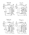
- the invention can include liquid crystal display device 100 having a plurality of flag alphanumeric legends 105a-d informing the viewer of the status of some variable being monitored - (e.g., fuel level).
- a plurality of flags 105a-d is shown in FIGS. 20-21.
- device 101 combines a bar graph representation 106 (or any other analog indicator), with associated flags 107a-b, such that the same parameter is monitored by both the flags 107a-b and bar graph 106.
- the message 108a e.g. "OVERHEAT"
- message 108b e.g.
- NVMAL "NORMAL" to be displayed is either etched on the front plate of the device 101 or on an overlay, the message writing 108a or b being opaque and the surrounding portions of glass or overlay being transparent (or vice-versa). Accordingly, the message 108a or b is visible only when there is a change in optical properties causing the underlying liquid crystal to be light-colored so that the opaque message 108 is visible because of the contrast with bright surrounding areas visible through transparent portions of the overlay.
- the flag display device 100 comprises an address plate 110 and a load plate 120, which are maintained in closely spaced relation to each other (FIG. 21).
- the gap between the plates contains liquid crystal material, as described above for the first embodiment.
- an address electrode 112 (FIGS. 20 and 21), in the form of a sheet and extending over areas in which the optical appearance of flags 105a-d will vary.
- the address plate enables an input signal in the form of a substantially uniform electric field to be applied across the liquid crystal material. Since the address electrode 112 is substantially non-resistive, a voltage applied to it will be present over the entire area of the electrode. Connection of input terminal 113 to a source (not shown) of an input signal can be provided as described for the first embodiment (FIG. 3).
- FIG. 23 illustrates several address electrodes 114 and 116 , each covering the area beneath a separate flag 107a or 107b (FIGS. 22 and 23).
- the separate address electrodes 114 and 116 can be connected commonly at input terminal 115 so that each is at the same potential.
- resistor 117 may be connected between electrodes 114 and 116 with electrode 114 connected to input terminal 115. This latter arrangement enables certain flags 107a and b to be turned on for a longer time than others.
- first address electrode 114 is directly connected to a source while the other address electrode 116 is connected by resistance 117 cutting the voltage from the source in half, then the flag 107a associated with first address electrode 114 will only remain on for input voltage variations that are half as large as those needed to alter the optical properties of the other f(ag_107b.
- load resistor 118 is connected to load electrodes 119a and b.
- Load resistor 141 is connected to load electrodes 142.
- FIG. 20 there is deposited on the inner surface of load plate 120 a resistor 130 of predetermined length and configuration. Differing fixed voltages are placed on input terminals 132 and 134 in order to place a voltage gradient along resistor 130 (FIGS. 20 and 21).
- Separate leads 135a-d extend from selected locations along resistor 130 to each individual flag 105a-d.
- the leads 135a-d are substantially non-resistive and are electrically connected to load electrodes 122a-d (FIG. 20), which are non-resistive and can be in the form of a sheet or a series of strips.
- the load electrodes 122a-d extend over an area in which it is desired to vary the optical appearance of the flag 105a-d.
- the voltages existing at load electrodes 122a-d for each separate flag 105a-d will be fixed and distinct because of the fixed voltage placed across terminals 132 and 134 and the gradient created along resistor 130.
- liquid crystal material in the gap 111 between the address electrode 112 and the load electrodes 122a-d changes its optical properties whenever a significant potential difference exists between overlapping address and load electrodes.
- each of the flags 105a-d can have its load electrodes 122a-d connected via separate leads 135a-d to a different fixed voltage, only one of a series of separately connected flags 105a-d can possibly have a zero potential difference between its load electrode 122a-d and the address electrode 112. If several address electrodes 114 and 116 are kept at different potentials, it is possible to have effectively a zero potential at more than one at a time.
- the only flag 105b with different optical properties must have its load electrode 122b connected to the resistor 130 at a location where approximately 7 volts is constantly maintained.
- the other flags 105d, 105c and 105a will each be individually turned on (or off) in FIGS. 20 and 21 when the input voltage applied to the address electrode 112 is at approximately 2 volts, 4.5 volts, or 9 volts.
- the liquid crystal flag displays can be associated with the displays of bar graph analog indicators described above to provide display device 101 in FIGS. 22 and 23.
- the same input voltage can be applied to the address electrodes 140 and 114 of the two types of displays, or a common address electrode may even be used.
- an input voltage associated with a certain engine condition for example, can be used in generating a bar graph presentation 106 as well as a flags 107a and b - (FIG. 22).
- the flag display 101 can use liquid crystal material which exhibits different optical properties as long as a certain threshold voltage is exceeded.
- this type of liquid crystal material were used in FIG. 20 and 2 volts was the threshold voltage of the liquid crystal material, an input voltage of 7 volts would cause the bottom two flags 105c and 105d to be turned on while the top two flags 105a and b remained off (or vice-versa).
- the same resistor 141 can be used for connection to the load electrodes 119a and b and also for connection to conductive strips 142, which are adapted to form an analog indicator presentation.
- variable optical properties of the material available for use in the viewing screen enable light transmission to be controlled in several different modes.
- transmission embodies each of the following methods of displaying waveforms: (1) a transmissive liquid crystal material, which is either transparent or opaque, is used and either (a) the view and light source (artificial or ambient) are on opposite sides of the viewing screen, or (b) the viewer and light source are on the same side of the viewing screen, with one of the surfaces on the plate farthest from the viewer being reflective; (2) a reflective liquid crystal material, which is either reflective or light absorbing, is used and the viewer and light source are on the same side of the viewing screen; (3) a transflective liquid crystal material, which is either transparent or reflective, is used and either (a) the viewer and light source are on opposite sides of the screen, or (b) the viewer and light source are on the same side of the viewing screen, with one of the surfaces on the plate farthest from the viewer being light absorbing; and (4) a light emitting material, which
- the presence of a sufficient electric field will cause the material to exhibit one of the two optical properties described above as possible for that type (e.g., transmissive, reflective, transflective) of liquid. crystal material-.-
- a sufficient electric field will cause the material to exhibit one of the two optical properties described above as possible for that type (e.g., transmissive, reflective, transflective) of liquid. crystal material-.-
- the load lines 60 can be placed in various configuration to simulate indicators commonly associated with certain measured parameters.
- FIG. 4 illustrates the configuration for a horizontal bar graph display.
- possible displays include fuel level (FIG. 12), voltage, current, oil pressure, temperature, and engine RPM as well as vehicle velocity indicators.
- the voltage signals applied to the address and load plates are analog. There is no need for drivers, multiplexers, decoders, or analog-to-digital converters in producing the display in accordance with the invention.
Landscapes
- Physics & Mathematics (AREA)
- General Physics & Mathematics (AREA)
- Liquid Crystal Display Device Control (AREA)
- Liquid Crystal (AREA)
- Devices For Indicating Variable Information By Combining Individual Elements (AREA)
Applications Claiming Priority (2)
| Application Number | Priority Date | Filing Date | Title |
|---|---|---|---|
| US72228985A | 1985-04-11 | 1985-04-11 | |
| US722289 | 1985-04-11 |
Publications (2)
| Publication Number | Publication Date |
|---|---|
| EP0205235A2 true EP0205235A2 (de) | 1986-12-17 |
| EP0205235A3 EP0205235A3 (de) | 1988-09-21 |
Family
ID=24901219
Family Applications (1)
| Application Number | Title | Priority Date | Filing Date |
|---|---|---|---|
| EP86302570A Withdrawn EP0205235A3 (de) | 1985-04-11 | 1986-04-07 | Verfahren und Vorrichtung für Flüssigkristallaufzeichnung von Analogindikatoren |
Country Status (2)
| Country | Link |
|---|---|
| EP (1) | EP0205235A3 (de) |
| JP (1) | JPS61259226A (de) |
Cited By (2)
| Publication number | Priority date | Publication date | Assignee | Title |
|---|---|---|---|---|
| WO2005073790A1 (en) * | 2004-01-26 | 2005-08-11 | Koninklijke Philips Electronics N.V. | Liquid crystal display device |
| CN108663555A (zh) * | 2017-03-29 | 2018-10-16 | 苏州普源精电科技有限公司 | 一种数字示波器的波形搜索方法及数字示波器 |
Family Cites Families (4)
| Publication number | Priority date | Publication date | Assignee | Title |
|---|---|---|---|---|
| CH527427A (de) * | 1971-02-15 | 1972-08-31 | Bbc Brown Boveri & Cie | Anordnung zur lokalen Änderung der optischen Eigenschaften einer Anzeigeschrift mittels einer Steuerspannung |
| US3820875A (en) * | 1972-04-14 | 1974-06-28 | W Bohmer | Scanner devices utilizing field effect light scattering dielectrics |
| US4112361A (en) * | 1975-06-05 | 1978-09-05 | Tokyo Seimitsu Co. Ltd. | Liquid crystal applied voltmeter |
| DE2724343A1 (de) * | 1977-05-28 | 1978-12-07 | Battelle Institut E V | Messgeraet fuer elektrische spannungen |
-
1986
- 1986-04-07 EP EP86302570A patent/EP0205235A3/de not_active Withdrawn
- 1986-04-11 JP JP8402186A patent/JPS61259226A/ja active Pending
Cited By (2)
| Publication number | Priority date | Publication date | Assignee | Title |
|---|---|---|---|---|
| WO2005073790A1 (en) * | 2004-01-26 | 2005-08-11 | Koninklijke Philips Electronics N.V. | Liquid crystal display device |
| CN108663555A (zh) * | 2017-03-29 | 2018-10-16 | 苏州普源精电科技有限公司 | 一种数字示波器的波形搜索方法及数字示波器 |
Also Published As
| Publication number | Publication date |
|---|---|
| JPS61259226A (ja) | 1986-11-17 |
| EP0205235A3 (de) | 1988-09-21 |
Similar Documents
| Publication | Publication Date | Title |
|---|---|---|
| KR100646898B1 (ko) | 지시계 | |
| US4448823A (en) | Multi-colored liquid crystal display device | |
| CN1046812C (zh) | 显示装置 | |
| EP0926468B1 (de) | Anzeigevorrichtung | |
| US4815824A (en) | Elliptical LCD bar graph with path outline-defining segments | |
| WO1985002703A1 (en) | A device for the presentation of information | |
| US4035060A (en) | Electro-optic device | |
| US4117472A (en) | Liquid crystal displays | |
| EP0070322A1 (de) | Flüssigkristall anzeigeeinheit | |
| JP4808314B2 (ja) | 液晶ディスプレイの駆動方法 | |
| US3979743A (en) | Displays | |
| EP0177134A2 (de) | Navigationsanzeigegerät mit Bildübertragung mit einem Flüssigkristall | |
| JPH027021A (ja) | オプトエレクトロニックマトリクス形指示装置 | |
| EP0205235A2 (de) | Verfahren und Vorrichtung für Flüssigkristallaufzeichnung von Analogindikatoren | |
| JPH07271310A (ja) | 車両用表示装置 | |
| US4306233A (en) | Electrical display device | |
| US4193669A (en) | Liquid crystal device for direct display of analog information | |
| JPS61107330A (ja) | フイルム感度及び閃光有効距離の表示装置 | |
| CA2013776C (en) | Electro-optic cell for animated displays and indicators | |
| DE2454203A1 (de) | Zusatzgeraet mit signalgeber fuer ein messinstrument | |
| JPH08509305A (ja) | 地図用情報を表示するための装置 | |
| EP1079209B1 (de) | Zeigerinstrument | |
| EP1510995A2 (de) | Anzeigevorrichtung | |
| JPS6019485B2 (ja) | 液晶表示装置の表示方法 | |
| DE102011086269A1 (de) | Kombinationsanzeigeinstrument in einem Fahrzeug |
Legal Events
| Date | Code | Title | Description |
|---|---|---|---|
| PUAI | Public reference made under article 153(3) epc to a published international application that has entered the european phase |
Free format text: ORIGINAL CODE: 0009012 |
|
| AK | Designated contracting states |
Kind code of ref document: A2 Designated state(s): DE FR GB IT NL |
|
| PUAL | Search report despatched |
Free format text: ORIGINAL CODE: 0009013 |
|
| AK | Designated contracting states |
Kind code of ref document: A3 Designated state(s): DE FR GB IT NL |
|
| RAP1 | Party data changed (applicant data changed or rights of an application transferred) |
Owner name: CONTROL INTERFACE CORPORATION |
|
| STAA | Information on the status of an ep patent application or granted ep patent |
Free format text: STATUS: THE APPLICATION IS DEEMED TO BE WITHDRAWN |
|
| 18D | Application deemed to be withdrawn |
Effective date: 19880922 |
|
| RIN1 | Information on inventor provided before grant (corrected) |
Inventor name: BOHMER, WILLIAM |