EP0201876A2 - Reihenschwingkreis-Umrichter - Google Patents
Reihenschwingkreis-Umrichter Download PDFInfo
- Publication number
- EP0201876A2 EP0201876A2 EP86106338A EP86106338A EP0201876A2 EP 0201876 A2 EP0201876 A2 EP 0201876A2 EP 86106338 A EP86106338 A EP 86106338A EP 86106338 A EP86106338 A EP 86106338A EP 0201876 A2 EP0201876 A2 EP 0201876A2
- Authority
- EP
- European Patent Office
- Prior art keywords
- resonant
- series
- power supply
- capacitor
- parallel
- Prior art date
- Legal status (The legal status is an assumption and is not a legal conclusion. Google has not performed a legal analysis and makes no representation as to the accuracy of the status listed.)
- Granted
Links
- 239000003990 capacitor Substances 0.000 claims abstract description 152
- 238000004804 winding Methods 0.000 claims description 13
- 239000004065 semiconductor Substances 0.000 description 48
- 238000010586 diagram Methods 0.000 description 20
- 238000007599 discharging Methods 0.000 description 5
- 238000013459 approach Methods 0.000 description 3
- 238000010276 construction Methods 0.000 description 2
- 238000001914 filtration Methods 0.000 description 2
- 230000015556 catabolic process Effects 0.000 description 1
- 230000000694 effects Effects 0.000 description 1
- 230000000670 limiting effect Effects 0.000 description 1
Images


Classifications
-
- H—ELECTRICITY
- H02—GENERATION; CONVERSION OR DISTRIBUTION OF ELECTRIC POWER
- H02M—APPARATUS FOR CONVERSION BETWEEN AC AND AC, BETWEEN AC AND DC, OR BETWEEN DC AND DC, AND FOR USE WITH MAINS OR SIMILAR POWER SUPPLY SYSTEMS; CONVERSION OF DC OR AC INPUT POWER INTO SURGE OUTPUT POWER; CONTROL OR REGULATION THEREOF
- H02M3/00—Conversion of DC power input into DC power output
- H02M3/22—Conversion of DC power input into DC power output with intermediate conversion into AC
- H02M3/24—Conversion of DC power input into DC power output with intermediate conversion into AC by static converters
- H02M3/28—Conversion of DC power input into DC power output with intermediate conversion into AC by static converters using discharge tubes with control electrode or semiconductor devices with control electrode to produce the intermediate AC
- H02M3/325—Conversion of DC power input into DC power output with intermediate conversion into AC by static converters using discharge tubes with control electrode or semiconductor devices with control electrode to produce the intermediate AC using devices of a triode or a transistor type requiring continuous application of a control signal
- H02M3/335—Conversion of DC power input into DC power output with intermediate conversion into AC by static converters using discharge tubes with control electrode or semiconductor devices with control electrode to produce the intermediate AC using devices of a triode or a transistor type requiring continuous application of a control signal using semiconductor devices only
- H02M3/337—Conversion of DC power input into DC power output with intermediate conversion into AC by static converters using discharge tubes with control electrode or semiconductor devices with control electrode to produce the intermediate AC using devices of a triode or a transistor type requiring continuous application of a control signal using semiconductor devices only in push-pull configuration
- H02M3/3376—Conversion of DC power input into DC power output with intermediate conversion into AC by static converters using discharge tubes with control electrode or semiconductor devices with control electrode to produce the intermediate AC using devices of a triode or a transistor type requiring continuous application of a control signal using semiconductor devices only in push-pull configuration with automatic control of output voltage or current
-
- Y—GENERAL TAGGING OF NEW TECHNOLOGICAL DEVELOPMENTS; GENERAL TAGGING OF CROSS-SECTIONAL TECHNOLOGIES SPANNING OVER SEVERAL SECTIONS OF THE IPC; TECHNICAL SUBJECTS COVERED BY FORMER USPC CROSS-REFERENCE ART COLLECTIONS [XRACs] AND DIGESTS
- Y02—TECHNOLOGIES OR APPLICATIONS FOR MITIGATION OR ADAPTATION AGAINST CLIMATE CHANGE
- Y02B—CLIMATE CHANGE MITIGATION TECHNOLOGIES RELATED TO BUILDINGS, e.g. HOUSING, HOUSE APPLIANCES OR RELATED END-USER APPLICATIONS
- Y02B70/00—Technologies for an efficient end-user side electric power management and consumption
- Y02B70/10—Technologies improving the efficiency by using switched-mode power supplies [SMPS], i.e. efficient power electronics conversion e.g. power factor correction or reduction of losses in power supplies or efficient standby modes
Definitions
- This invention relates to a series resonant converter, which comprises a series resonant circuit, a rectifier in series therewith and a semiconductor switch and converts a DC voltage into a different DC voltage supplied to a load.
- a series resonant converter usually has two resonant loops each of which comprises a series resonant circuit consisting of an inductor and a capacitor, a rectifier connected in series with the series resonant circuit and a switch element, e.g., a bipolar transistor (or MOS transistor) or a diode.
- the resonant current flowing through the switch element has a sinusoidal waveform and naturally turns to zero, so that the switch element need not forcibly turn the current off. Theoretically, therefore, there is no switching loss.
- less noise is produced, and it is possible to readily construct the converter operable at a high frequency.
- it can be expected to obtain a noise-free, small size and light weight converter.
- the output characteristics of the series resonant circuit are essen-" tially constant current characteristics. Therefore, the converter system can be readily protected in case when there occurs an overload or a short-circuit in the load.
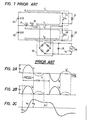
- Fig. 1 shows a prior art series resonant converter which is disclosed in, for instance, W. Mc Murray, "The Thyristor Electronic Transformer: A Power Converter Using a High Frequency Link", IEEE Transaction on IGA, No. 4, PP. 451-457.
- Figs. 2A, 2B and 2C are waveform diagrams illustrating the operation of the converter.
- reference numeral 11 designates a semiconductor switch, which is a transistor and serves as a switch element.
- semiconductor switch 11 When semiconductor switch 11 is turned on by application of a gate signal to the gate of transistor 11, series resonant current i 1 (shown by solid line) is caused to flow through a series resonant loop extending from power supply 12 through semiconductor switch 11, rectifier 13, load 14 (capacitor 15), then rectifier 13 again, then capacitor 16 and inductor 17 to return to power supply 12.
- This series resonant current i l is sinusoidal as shown in Fig. 2A.
- This current i 1 again is a series resonant current through inductor 17 and capacitor 16 and after a period ⁇ LoCo from its start, turns to zero.
- the gate signal is arranged to have a duration longer than ⁇ LoCo and shorter than 2 ⁇ /LoCo. Therefore, the gate signal having been applied to transistor 11 is removed within the period of current i 1 , preventing from generation of further resonant current after the cease of i 1 .
- the currents i l and i 1 are full-wave rectified through rectifier 13 so that current i3 flows through capacitor 15 for filtering as shown in Fig. 2B. Capacitor 15 continuously supplies a DC voltage across load 14.
- Reference numeral 18 designates another semiconductor switch, which also is a transistor and serves as a switch element.
- series resonant current i 2 (shown by solid line) is caused to flow through a series resonant loop extending from power supply 19 through inductor 17, capacitor 16, rectifier 13, load 14 (capacitor 15), then rectifier 13 again, and then semiconductor switch 18 to return to power supply 19.
- This series resonant current i 2 is shown in Fig. 2A. After i 2 has once become zero, current i 2 flows through diode 22. Rectifier 13 rectifies these currents i 2 and i 2 ' to provide current i3 for charging capacitor 15 for filtering. That is, capacitor 13 supplies a DC voltage to load 14.
- currents i l and i 2 are series resonant currents equal in magnitude and opposite in polarity to each other.
- series resonant currents i 1 and i 2 are equal in magnitude and opposite in polarity to each other.
- a gate signal generating circuit generates two gate signals of a frequency f with 180° out of phase from each other and supplied to the respective gates of switches 11 and 18, and the output voltage V o is fed back to the signal generating circuit to control the frequency f of the gate signals so as to maintain the output voltage Vo constant. Therefore, frequency f lowers as resistance R increases, as will be seen from equation (3), and in the case of light load operation, the frequency may easily enter an audio frequency range. For example, if operating frequency f is 100 kHz under the rated current (100 % load) condition, a load reduction to 20 % load or less would cause the frequency f to become lower than 20 kHz, giving rise to noisy sounds. It has been difficult to cope with the noise because the operating frequency changes with the load.
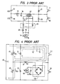
- F ig. 3 shows a series resonant converter proposed in Electronic Engineering, Sep. 1981, page 39 to solve the problems discussed above.
- a series circuit consisting of the primary winding of transformer 27 and capacitor 16 is connected between the connection point between switch elements 11 and 18 and one terminal of inductor 17.
- DC power sources 12 and 19 are connected between the other terminal of inductor 17 and the other terminals of respective switch elements 11 and 18.
- Capacitor 44 is connected in parallel with the secondary winding of transformer 27, and rectifier 13, inductor 20 and load 14 are connected in series with the secondary winding of transformer 27.
- the current in the series resonant circuit at a frequency higher than f o is inversely proportional to the frequency. Therefore, it is possible to obtain constant voltage control through switching frequency control such that the switching frequency is increased with reducing load current and reduced with increasing load current in a range above f o .
- capacitor 44 is connected across the secondary winding of transformer 27, and series inductor 20 is connected between the output of rectifier 13 and one terminal of capacitor 15, whereby a sinusoidal voltage is transmitted to the. secondary side of transformer 27.
- a considerably large reactive current flows through capacitor 44 without being substantially influenced by the load.
- a substantial portion of current flowing through switch elements 11 and 18 under a light load condition is a reactive current flowing through transformer 27 to capacitor 44, so that the efficiency is extremely reduced.
- Fig. 4 shows a further well-known series resonant converter.
- diodes 21 and 22 are connected in parallel with respective capacitors 41 and 42, DC power supply 43 is applied across the series connection of capacitors 41 and 42, and rectifier 13 is serially connected between the junction of semiconductor switches 11 and 18 and inductor 17.
- the gates of transistors (i.e. switch elements) 11 and 18 are controlled by gate signals having a frequency and a 50 % duty ratio, with 180° out of phase from each other.
- This converter has a feature that the endurable voltage (i.e. breakdown voltage) required for semiconductor switches 11 and 18 and resonant capacitors 41 and 42 may suffice if selected to be higher than the voltage across power supply 43.
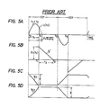
- FIG. 5 shows waveforms obtained in various parts of the converter of Fig. 4.
- charging current i l flows from power supply 43 through semiconductor switch 11, rectifier 13, load 14 (capacitor 15), then rectifier 13 again, and then resonant inductor 17 to charge resonant capacitor 42.
- discharging current i 2 from resonant capacitor 41 flows through semiconductor switch 11, rectifier 13, load 14 (capacitor 15), then rectifier 13 again, and then resonant capacitor 17.
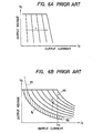
- the output voltage V o versus output current I o characteristic is a constant current characteristic as shown in Fig. 6A; that is, output current I o is substantially constant regardless of reduction of output voltage V o so long as the operating frequency f is constant.
- the average of currents i i , i 2 and i 2 flowing into rectifier 13, i.e. output current I o is proportional to capacitance C o operating frequency f and inversely proportional to output voltage V o as shown in Fig. 6B.
- a primary object of the invention is to provide a series resonant converter, which permits to set a lowest allowable frequency to change in the operating frequency relative to load variations and which is free from noise.
- a second object of the invention is to provide a series resonant converter, which permits constant voltage control for over a range from zero to full load and has a narrow operating frequency range as well as capability of holding the operating frequency above a lowest allowable frequency.
- a third object of the invention is to provide a series resonant circuit, which can limit the output voltage without noise generation even when the output voltage is extraordinarily reduced due to such cause as an output short-circuit.
- parallel resonant means having a resonant frequency above the audible frequency is connected in series with a rectifier of the series resonant converter, that is, the parallel resonant means is inserted in each series resonant loop.
- a capacitor is provided in series with the rectifier of the series resonant converter.
- the operating frequency is reduced to limit corresponding output current increase.
- series resonance produced by the capacitor noted above and a resonant inductor effects so that the output current is automatically cut off at zero crossing of the resonant current.
- the output current thus will not be extraordinarily increased, so that there is no need of reducing the operating frequency to be in the audible frequency range.
- a rectifier is provided commonly for a first series resonant loop including a first switch element and a second series resonant loop including a second switch element.
- Power supply means is provided such that a resonant current is caused to flow through the first series resonant loop through control of the first switch element and a resonant current is caused to flow through the second series resonant loop through control of the second switch element.
- parallel resonant means is provided for each of the first and second series resonant loops. The resonant frequency of the parallel resonant means is selected to be the lowest operating frequency (higher than the audible frequency range).
- a power supply may be provided for each of or commonly for the first and second series resonant loops.
- a capacitor or an inductor or both of them may be used commonly for the first and second series resonant loops.
- current is caused to flow from the power supply to the first series resonant loop through control of the first switch element, and energy stored at this time is then supplied through the second switch element to the second series resonant loop to cause therein a resonant current.
- no power supply may be inserted in the second series resonant loop.
- a series resonant capacitor and a series resonant inductor may be provided commonly for or for each of the first and second series resonant loops.
- diodes are connected in parallel with the respective first and second switch elements. The resonant current is supplied to the rectifier not only when a switch element is turned on but also when the switch element is turned off.
- a rectifier is provided commonly for a first series resonant loop including a first switch element and a second series resonant loop including a second switch element.
- the first and second switch elements are connected in series, and a power supply is connected across these series switch elements.
- a diode is connected in parallel with a resonant capacitor of the first series resonant loop such that it has the opposite polarity to the power supply.
- a second diode is connected in parallel with a resonant capacitor of the second series resonant loop such ' that it has the opposite polarity to the power supply.
- a third capacitor is provided for each of or commonly for the first and second series resonant loops.
- the capacitance of the third capacitor is selected such that the resonant frequency of the circuit consisting of this third capacitor and a resonant inductor of the first or second series resonant loop is sufficiently lower than the series resonant frequency of each series resonant loop.
- Fig. 7 is a circuit diagram showing a first embodiment of a first aspect of the invention.
- This embodiment of the series resonant converter is an improvement over the prior art series resonant converter shown in Fig. 1 in that parallel resonant circuit 23 consisting of inductor 24 and capacitor 25 is connected in series with series resonant circuit 26 consisting of capacitor 16 and inductor 17.
- parallel resonant circuit 23 consisting of inductor 24 and capacitor 25
- series resonant circuit 26 consisting of capacitor 16 and inductor 17.
- the impedance of parallel resonant circuit 23 is maximum at resonant frequency fp and is sharply reduced with increase of the operating frequency f beyond fp.
- the operation characteristic of the converter is substantially identical with that of Fig. 1.
- switch element e.g. semiconductor switch
- current i 1 is caused to flow through a loop extending from power supply 12 through semiconductor switch 11, rectifier 13, load 14 (capacitor 15), then rectifier 13 again, then capacitor 16, inductor 17 and parallel resonant circuit 23, whereby power is supplied to load 14.
- the resonant current ii of each sinusoidal half cycle has a duration of ⁇ /LoCo as shown in Fig. 2A.
- the repetition period of intermittent current i l through parallel resonant circuit 23 is the operating cycle period 1/f, with which semiconductor switches 11 and 18 are alternately turned on and off.
- each of gate signals for turning on switches 11 and 12 is selected to be longer than ⁇ /LoCo and shorter than 2 ⁇ LoCo.
- the impedance of parallel resonant circuit 23 is sufficiently low, so that the peak value of current i i is substantially constant regardless of the operating frequency as in the prior art converter shown in Fig. 1.
- the impedance of parallel resonant circuit 23 sharply increases to cause sharp reduction in peak value of current i l .
- switch element e.g. semiconductor switch
- resonant current i 2 is caused to flow from power supply 19 through parallel resonant circuit 23, inductor 17, capacitor 16, rectifier 13, load 14 (capacitor 15), then rectifier 13 again, and then semiconductor switch 18.
- Fig. 8 is a circuit diagram showing a second embodiment, where the invention is applied to a series resonant converter which employs a transformer for insulating DC input and DC output from each other.
- transformer 27 has the primary winding connected in series with series resonant circuit 26 and the secondary winding connected between the AC input terminals of rectifier 13.
- series resonant circuit 26 and rectifier 13 are connected in series with each other through transformer 27.
- a parallel resonant circuit is inserted in each of two series resonant loops. More specifically, parallel resonant circuits 23a and 23b are inserted between respective power supplies 12 and 19 and respective semiconductor switches 11 and 18.
- this second embodiment is the same as in the first embodiment shown in Fig. 7.
- the input and output sides can be insulated from each other, and the output voltage can be freely set according to turns ratio n l/ n 2 of transformer 27.
- Fig. 9 shows a third embodiment of the series resonant converter.
- This embodiment is such one where the invention is applied to the prior art converter shown in Fig. 4. More specifically, parallel resonant circuit 23 is connected in series with resonant inductor 17 between the connection point between switch elements 11 and 18 and the connection point between capacitors 41 and 42. The operation of this embodiment will be readily understood from the description in connection with Figs. 4 and 7, so that it will not be described.
- Fig. 10 shows a fourth embodiment of the series resonant converter.
- single power supply 43 and two resonant capacitors 41 and 42 are used.
- independent resonant inductors 17a and 17b are provided for the respective series resonant loops.
- Parallel resonant circuit 23 is connected between the connection point between resonant capacitors 41 and 42 and the connection point between switch elements 11 and 18. The operation is similar to that of the converter shown in Fig. 4, and it is readily conceivable that this converter permits clamping of the operating frequency at the resonant frequency of parallel resonant circuit 23 even if the load is extremely reduced.
- Fig. 11 shows a fifth embodiment of the series resonant converter.
- a series circuit consisting of parallel resonant circuit 23, series resonant circuit 26 and transformer 27 is connected between the connection point between switch elements 11 and 18 and one terminal of power supply 43.
- switch element 11 When switch element 11 is turned on, resonant current i l is caused to flow from power supply 43 through series resonant circuit 26, transformer 27 and parallel resonant circuit 23.
- resonant current i l becomes zero, the voltage across resonant capacitor 16 reaches a peak value higher than power supply voltage E. Therefore, resonant current i 1 ' as shown by dashed line starts flowing through diode 21 to discharge the voltage across capacitor 16 to the voltage E of power supply 43.
- Switch element 11 is turned off while the current i l ' is flowing.
- Switch element 18 is subsequently turned on, whereupon capacitor 16 is discharged through switch element 18.
- resonant current i 2 is caused to flow until resonant capacitor 16 is charged in opposite direction to a certain extent.
- capacitor 16 starts to discharge in the opposite direction, whereby a resonant current i 2 flows through diode 22.
- resonant currents i l and i 2 can be sufficiently suppressed when the operating frequency becomes the resonant frequency fp of parallel resonant circuit 23 with a load reduction.
- Fig. 12 shows a sixth embodiment of the series resonant converter.
- the inductance of a transformer is utilized as a series resonant inductor, and energy is once stored in the transformer before being discharged through rectifier 13 to load 14 (15).
- transformer 46 has the primary winding having the opposite terminals connected through respective switch elements 11 and 18 to the opposite terminals of power supply 43.
- a series circuit consisting of resonant capacitor 16 and parallel resonant circuit 23 is connected between a center tap of the primary winding and one of the terminals of power supply 43. Whan switch element 11 is turned on, series resonant current i 1 is caused, which is determined by the primary winding of transformer 46 and resonant capacitor 16.
- switch element 11 After current i i becomes zero, switch element 11 is turned off, where upon capacitor 15 is charged by energy stored in transformer 46 through rectifier 13.
- switch element 18 When switch element 18 is turned on, resonant capacitor 16 is discharged through trnasformer 46. At this time, resonant current i 2 is caused. When resonant current i 2 becomes zero, switch element 18 is turned off, whereupon capacitor 15 is charged by energy stored in transformer 46 through rectifier 13.
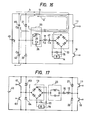
- Fig. 13 shows an embodiment according to a second aspect of the invention. This embodiment is an improvement over the prior art series resonant converter shown in Fig. 4 in that third resonant capacitor 47 is connected in series with rectifier 13.
- Fig. 14 shows waveforms produced in various parts of the converter shown in ' Fig. 13.
- This current i2 is a resonant current resulting from resonance by resonant inductor 17 and third resonant capacitor 47, and has, if exterpolated, a sinusoidal waveform with a half cycle period time of ⁇ /2LoCs, and becomes zero after the lapse of time T 2 .
- Time period T 2 is can be freely set by suitably selecting capacitance Cs of third resonant capacitor 47.
- semiconductor switch 18 is turned on to charge resonant capacitor 41 and discharge resonant capacitor 42.
- this embodiment of the converter operates in the manner as described above, when output voltage V o is reducing, the current through semiconductor switch 11 (or 18) can be forcibly reduced to zero by making use of the resonance between resonant inductor 17 and third resonant capacitor 47 after it has been switched over to diode 21 (or 22), that is, the output current can be sufficiently limited.
- the output current thus can be sufficiently limited without need of reducing operating frequency to an audible frequency in case of occurrence of an overload or short-circuit.
- Third resonant capacitor 47 may be inserted in each series resonant loop independently.
- Fic. 15 shows an example of such arrangement. More specifically, in this instance semiconductor switch 11 and diode 21 are connected together through third resonant capacitor 47a on the side of power supply 43, while semiconductor switch 18 and diode 22 are connected together through third resonant capacitor 47b on the side of power supply 43. In this instance, the DC input and DC output are insulated from each other by transformer 27.
- Fig. 16 is a circuit diagram showing an embodiment of the first and second aspects of the invention applied to the prior art converter shown in Fig. 4.
- F ig. 16 parts like those in Figs. 4, 7 and 13 are designated by like reference numerals.
- parallel resonant circuit 23 and third resonant capacitor 47 are connected in series with rectifier 13.
- resonant current i l is caused to charge resonant capacitor 42 from power supply 43 through semiconductor switch 11, rectifier 13, load 14 (capacitor 15), then rectifier 13 again, then third resonant capacitor 47, resonant inductor 17 and parallel resonant circuit 23.
- discharging current i 2 is caused to flow from resonant capacitor 41 through semiconductor switch 11, rectifier 13, load 14 (capacitor 15), then rectifier 13 again, then third resonant circuit 47, resonant inductor 17 and parallel resonant circuit 23.
- This current i2 is a resonant current provided by resonant inductor 17, capacitor 25 of parallel resonant circuit 23 and third resonant capacitor 47. Since the capacitance of resonant capacitor 25 is determined by the conditions for the lowest frequency clamping, i2 can be freely set by suitably selecting the capacitance of third resonant capacitor 47. In the above way, one half cycle of operation is completed. In the next half cycle, semiconductor switch 18 is turned on to cause charging of resonant capacitor 41 and discharging of resonant capacitor 42.
- Resonant capacitor 47 is effective mainly after the turning-on of diode 21 (or 22) to extinguish resonant current i2 caused by resonant inductor 17. After the turning-on of diode 21 (or 22), the current i 2 ' having been flowing through resonant inductor 17 is consumed only in load 14. In the prior art series resonant converter such as shown in Fig. 4, even when the output voltage becomes low, the current i 2 noted above does not become zero because the load is low.
- the semiconductor switch is not naturally turned off, resulting in extraordinary increase of the output current.
- the semiconductor switch has to be forcibly turned off, which gives rise to other problems as discussed before.
- the resonant current i 2 after the diode 21 (or 22) has been turned on is naturally reduced to zero using the resonance between third resonant capacitor 47 and resonant inductor 17.
- it is possible to sufficiently limit the output current by suitably selecting the capacitance of third resonant capacitor 47 to solve the various provlems noted above.
- the operating frequency is lowered to reduce the output current.
- the lower limit of the operating frequency is selected to be parallel resonant frequency fp of parallel resonant circuit 23.
- fp is set to a suitable value above the audible frequency range, e.g., 20 kHz, the resonant converter can be operated at a frequency higher than audible frequency range even when the load is very light because with reduction of the operating frequency to fp the output current becomes sufficiently small.
- single semiconductor switch 11 is provided in the first series resonant loop, and single semiconductor switch 18 in the second series resonant loop.
- power supply 43 is connected across a series combination of switch elements 11 and 18 and also across a series combination of switch elements 61 and 62.
- Diodes 63 and 64 are connected in parallel with respective switch elements 61 and 62 such that they are of the opposite polarity to the power supply 43.
- a series connection of parallel resonant circuit 23, resonant inductor 17, resonant capacitor 16, and rectifier 13 are connected between the connection point between switch elements 11 and 18 and the connection point between switch elements 61 and 62.
- switch elements 18 and 61 are turned off and switch elements 11 and 62 are simultaneously turned on to bring about a similar operation. Again in this case, with a reduction of the load the repetition frequency, at which switch elements 11 and 62 are turned on and then switches 18 and 61 are simultaneously turned on, is reduced. This frequency reduction, however, is allowed only in the range above the parallel resonant frequency by resonance of parallel resonant circuit 23.
- a parallel resonant circuit which makes the lower limit of the operating frequency (selected to a value above the audible frequency range) as resonant frequency, is provided in each of or commonly for the two series resonant loops. Therefore, when operating frequency is reduced to the lower limit under a very light load condition, the impedance of the series resonant loops is sufficiently increased to limit the output current.
- the converter thus can be used even under a very light load condition. Besides, neither noise is generated, nor wasteful current is caused to ensure high efficiency. Further, the operating frequency range may be narrow, and the construction of the operating frequency control circuit may be simple.
- third resonant capacitor is provided for each of or commonly for the two series resonant loops, and series resonant frequency fs of the circuit constituted by the third resonant capacitor and a series resonant inductor is set to be lower than series resonant frequency f o given by series resonant inductor and series resonant capacitor.
- series resonant frequency fs of the circuit constituted by the third resonant capacitor and a series resonant inductor is set to be lower than series resonant frequency f o given by series resonant inductor and series resonant capacitor.
- a series resonant converter according to both the first and second aspects of the invention will be free from noise regardless of whether the load is light or heavy and may have a narrow operating frequency control range.
Landscapes
- Engineering & Computer Science (AREA)
- Power Engineering (AREA)
- Dc-Dc Converters (AREA)
- Inverter Devices (AREA)
Applications Claiming Priority (6)
| Application Number | Priority Date | Filing Date | Title |
|---|---|---|---|
| JP98997/85 | 1985-05-10 | ||
| JP9899785A JPH0697839B2 (ja) | 1985-05-10 | 1985-05-10 | 直列共振コンバ−タ |
| JP45725/86 | 1986-03-03 | ||
| JP4572586A JPH0626468B2 (ja) | 1986-03-03 | 1986-03-03 | 直列共振コンバ−タ |
| JP61099807A JPH0710170B2 (ja) | 1986-04-28 | 1986-04-28 | 直列共振コンバ−タ |
| JP99807/86 | 1986-04-28 |
Publications (3)
| Publication Number | Publication Date |
|---|---|
| EP0201876A2 true EP0201876A2 (de) | 1986-11-20 |
| EP0201876A3 EP0201876A3 (en) | 1987-12-02 |
| EP0201876B1 EP0201876B1 (de) | 1993-03-17 |
Family
ID=27292355
Family Applications (1)
| Application Number | Title | Priority Date | Filing Date |
|---|---|---|---|
| EP86106338A Expired - Lifetime EP0201876B1 (de) | 1985-05-10 | 1986-05-07 | Reihenschwingkreis-Umrichter |
Country Status (3)
| Country | Link |
|---|---|
| US (1) | US4679129A (de) |
| EP (1) | EP0201876B1 (de) |
| DE (1) | DE3687999T2 (de) |
Cited By (1)
| Publication number | Priority date | Publication date | Assignee | Title |
|---|---|---|---|---|
| EP0332436A3 (en) * | 1988-03-11 | 1990-06-27 | Origin Electric Co. Ltd. | Series resonant power converter and method of controlling the same |
Families Citing this family (47)
| Publication number | Priority date | Publication date | Assignee | Title |
|---|---|---|---|---|
| DE3606462A1 (de) * | 1986-02-28 | 1987-09-03 | Leybold Heraeus Gmbh & Co Kg | Wechselrichter mit einem gleichspannungsteil und einem zerhackerteil |
| US4860184A (en) * | 1987-09-23 | 1989-08-22 | Virginia Tech Intellectual Properties, Inc. | Half-bridge zero-voltage switched multi-resonant converters |
| US4833584A (en) * | 1987-10-16 | 1989-05-23 | Wisconsin Alumni Research Foundation | Quasi-resonant current mode static power conversion method and apparatus |
| US4914559A (en) * | 1988-01-19 | 1990-04-03 | American Telephone And Telegraph Company | Power factor improving arrangement |
| IL85138A (en) * | 1988-01-19 | 1991-04-15 | Arie Lieberman | Dc to dc power converter |
| US5019959A (en) * | 1988-09-19 | 1991-05-28 | Innovative Controls, Inc. | Ballast circuit |
| US4945466A (en) * | 1989-02-22 | 1990-07-31 | Borland Walter G | Resonant switching converter |
| US4972309A (en) * | 1989-03-14 | 1990-11-20 | Hughes Aircraft Company | N-phase sinewave converter |
| US5057698A (en) * | 1989-11-13 | 1991-10-15 | Exide Electronics | Shunt circuit for reducing audible noise at low loading conditions of a power supply employing a high frequency resonant converter |
| US5208738A (en) * | 1990-12-13 | 1993-05-04 | Northern Telecom Limited | Constant frequency resonant DC/DC converter |
| US5157593A (en) * | 1990-12-13 | 1992-10-20 | Northern Telecom Limited | Constant frequency resonant dc/dc converter |
| US5113337A (en) * | 1991-02-08 | 1992-05-12 | General Electric Company | High power factor power supply |
| FI87412C (fi) * | 1991-02-25 | 1992-12-28 | Kemppi Oy | Svetsningsinverter och foerfarande foer styrning av svetsningsinverter |
| US5140510A (en) * | 1991-03-04 | 1992-08-18 | Motorola, Inc. | Constant frequency power converter |
| JP2722869B2 (ja) * | 1991-06-11 | 1998-03-09 | ヤマハ株式会社 | 電源回路 |
| US5159541A (en) * | 1991-10-31 | 1992-10-27 | Northern Telecom Limited | Asymmetrical pulse width modulated resonant DC/DC converter |
| US5267138A (en) * | 1992-03-23 | 1993-11-30 | Creos International Ltd. | Driving and clamping power regulation technique for continuous, in-phase, full-duration, switch-mode resonant converter power supply |
| JP3151932B2 (ja) * | 1992-04-27 | 2001-04-03 | ヤマハ株式会社 | 電源回路 |
| US5412557A (en) * | 1992-10-14 | 1995-05-02 | Electronic Power Conditioning, Inc. | Unipolar series resonant converter |
| WO1994014230A1 (en) * | 1992-12-07 | 1994-06-23 | Exide Electronics Corporation | Series resonant converter having a three part resonant inductor |
| US5438497A (en) * | 1993-05-13 | 1995-08-01 | Northern Telecom Limited | Tertiary side resonant DC/DC converter |
| DE4334592C1 (de) * | 1993-10-11 | 1994-07-21 | Siemens Ag | Hochfrequenz-Generator |
| US5638260A (en) * | 1995-05-19 | 1997-06-10 | Electronic Measurements, Inc. | Parallel resonant capacitor charging power supply operating above the resonant frequency |
| US5684678A (en) | 1995-12-08 | 1997-11-04 | Delco Electronics Corp. | Resonant converter with controlled inductor |
| US5715155A (en) * | 1996-10-28 | 1998-02-03 | Norax Canada Inc. | Resonant switching power supply circuit |
| US5768112A (en) * | 1997-05-30 | 1998-06-16 | Delco Electronics Corp. | Sub-resonant series resonant converter having improved form factor and reduced EMI |
| DE19823917A1 (de) * | 1997-06-03 | 1998-12-10 | Fuji Electric Co Ltd | Stromrichtervorrichtung |
| US6181116B1 (en) * | 1998-05-22 | 2001-01-30 | Nmb U.S.A. Inc. | Power regulator |
| DE19955673A1 (de) * | 1999-11-19 | 2001-05-23 | Philips Corp Intellectual Pty | Leistungsversorgungseinheit mit einem Wechselrichter |
| WO2001076053A1 (en) * | 2000-04-03 | 2001-10-11 | Aalborg Universitet | A resonant converter |
| DE10038814A1 (de) * | 2000-08-09 | 2002-02-21 | Abb Research Ltd | Hochspannungs-Gleichstromwandler |
| US6496396B2 (en) * | 2001-02-09 | 2002-12-17 | Tyco Electronics Logistics Ag | Reverse recovery circuit, method of operation thereof and asymmetrical half-bridge power converter |
| DE10139445A1 (de) * | 2001-08-10 | 2003-02-20 | Philips Corp Intellectual Pty | Netzgerät |
| US6487099B1 (en) * | 2001-08-24 | 2002-11-26 | Northrop Grumman Corporation | Time compensated current ramp for resonant power converters |
| DE10159897A1 (de) * | 2001-12-06 | 2003-06-26 | Philips Intellectual Property | Spannungsversorgung für Röntgengenerator |
| WO2003098789A1 (en) * | 2002-05-16 | 2003-11-27 | Intreprinderea Mixta Moldo-Rusa 'elcon' S.R.L. | A regulated resonant voltage converter and a method of regulated resonance dc-dc voltage conversion |
| GB2393336B (en) * | 2002-09-20 | 2005-07-20 | Coutant Lambda Ltd | Multi-resonant power conversion apparatus and methods |
| JP4345294B2 (ja) * | 2002-12-09 | 2009-10-14 | 富士ゼロックス株式会社 | 電源装置及び画像形成装置 |
| MD3850C2 (ro) * | 2007-04-12 | 2009-12-31 | Институт Электронной Инженерии И Промышленных Технологий Академии Наук Молдовы | Convertizor de tensiune continuă cu cvasirezonanţă |
| MD3853C2 (ro) * | 2007-05-10 | 2009-12-31 | Институт Электронной Инженерии И Промышленных Технологий Академии Наук Молдовы | Convertizor de tensiune cu rezonanţă |
| MD3851C2 (ro) * | 2007-07-25 | 2009-12-31 | Институт Электронной Инженерии И Промышленных Технологий Академии Наук Молдовы | Convertizor de tensiune cu cvasirezonanţă |
| MD215Z (ro) * | 2007-10-16 | 2010-12-31 | Институт Электронной Инженерии И Промышленных Технологий Академии Наук Молдовы | Dispozitiv de încărcare a acumulatorului capacitiv |
| MD20070283A (ro) * | 2007-10-16 | 2009-07-31 | Институт Электронной Инженерии И Промышленных Технологий Академии Наук Молдовы | Procedeu de formare a curentului de încărcare pentru un acumulator de energie capacitiv |
| JP4232845B1 (ja) * | 2007-10-19 | 2009-03-04 | サンケン電気株式会社 | 直流変換装置 |
| MD4073C1 (ro) * | 2008-11-06 | 2011-05-31 | Институт Электронной Инженерии И Промышленных Технологий Академии Наук Молдовы | Convertizor stabilizat de tensiune înaltă |
| US9143043B2 (en) | 2012-03-01 | 2015-09-22 | Infineon Technologies Ag | Multi-mode operation and control of a resonant converter |
| RU2749280C1 (ru) * | 2020-11-02 | 2021-06-08 | Акционерное общество "Научно-производственный центр "Полюс" | Резонансный преобразователь постоянного напряжения с повышенными надежностью и КПД |
Family Cites Families (5)
| Publication number | Priority date | Publication date | Assignee | Title |
|---|---|---|---|---|
| US4054827A (en) * | 1976-04-12 | 1977-10-18 | The United States Of America As Represented By The Secretary Of The Army | Voltage boost circuit for DC power supply |
| US4035745A (en) * | 1976-05-13 | 1977-07-12 | Sachs-Systemtechnik Gmbh | Circuit for the production of an open alternating magnetic field |
| DE2901326A1 (de) * | 1979-01-15 | 1980-07-24 | Sachs Systemtechnik Gmbh | Sinusleistungsgenerator |
| US4263642A (en) * | 1979-03-28 | 1981-04-21 | Litton Systems, Inc. | DC to DC converter |
| JPS58123369A (ja) * | 1982-01-14 | 1983-07-22 | Matsushita Electric Ind Co Ltd | 定電圧電源装置 |
-
1986
- 1986-05-05 US US06/859,680 patent/US4679129A/en not_active Expired - Lifetime
- 1986-05-07 DE DE8686106338T patent/DE3687999T2/de not_active Expired - Lifetime
- 1986-05-07 EP EP86106338A patent/EP0201876B1/de not_active Expired - Lifetime
Cited By (1)
| Publication number | Priority date | Publication date | Assignee | Title |
|---|---|---|---|---|
| EP0332436A3 (en) * | 1988-03-11 | 1990-06-27 | Origin Electric Co. Ltd. | Series resonant power converter and method of controlling the same |
Also Published As
| Publication number | Publication date |
|---|---|
| DE3687999T2 (de) | 1993-07-22 |
| EP0201876A3 (en) | 1987-12-02 |
| EP0201876B1 (de) | 1993-03-17 |
| DE3687999D1 (de) | 1993-04-22 |
| US4679129A (en) | 1987-07-07 |
Similar Documents
| Publication | Publication Date | Title |
|---|---|---|
| EP0201876A2 (de) | Reihenschwingkreis-Umrichter | |
| JP2774344B2 (ja) | 突入電流制限交直変換回路 | |
| US5508903A (en) | Interleaved DC to DC flyback converters with reduced current and voltage stresses | |
| US6031737A (en) | AC-DC power supply | |
| US5856916A (en) | Assembly set including a static converter with controlled switch and control circuit | |
| US6611444B2 (en) | Zero voltage switching DC-DC converter | |
| US5930122A (en) | Inverter and DC power supply apparatus with inverter used therein | |
| US4935857A (en) | Transistor conduction-angle control for a series-parallel resonant converter | |
| US6587358B1 (en) | Switching power supply circuit | |
| JP3459142B2 (ja) | 駆動パルス出力制限回路 | |
| CA2168520C (en) | Inverter/charger circuit for uninterruptible power supplies | |
| US6388902B1 (en) | Switching power supply circuit | |
| GB2137030A (en) | Regulated dc to dc converter | |
| US4158881A (en) | DC to DC converter | |
| US5864472A (en) | Apparatus for controlling a multiresonant self-oscillating converter circuit | |
| US4760512A (en) | Circuit for reducing transistor stress and resetting the transformer core of a power converter | |
| US5303137A (en) | Multiresonant self-oscillating converter circuit | |
| EP0058401A2 (de) | Schaltkreis mit hoher Schaltfrequenz | |
| EP0683936A1 (de) | Steuerschaltung für einen getakteten gleichspannungswandler mit einer gesteuerten magnetkern-rücksetztechnik zur ausgangsregelung | |
| US6166927A (en) | Push-pull power converter circuit | |
| US5986898A (en) | Switched-mode power supply with power factor correction | |
| US4445166A (en) | High voltage converter | |
| EP0058399B1 (de) | Hochfrequenter Schaltkreis | |
| JPH0320046Y2 (de) | ||
| US4875001A (en) | Electronic switching power supply with a choke converter |
Legal Events
| Date | Code | Title | Description |
|---|---|---|---|
| PUAI | Public reference made under article 153(3) epc to a published international application that has entered the european phase |
Free format text: ORIGINAL CODE: 0009012 |
|
| 17P | Request for examination filed |
Effective date: 19860507 |
|
| AK | Designated contracting states |
Kind code of ref document: A2 Designated state(s): DE GB SE |
|
| PUAL | Search report despatched |
Free format text: ORIGINAL CODE: 0009013 |
|
| AK | Designated contracting states |
Kind code of ref document: A3 Designated state(s): DE GB SE |
|
| 17Q | First examination report despatched |
Effective date: 19900615 |
|
| GRAA | (expected) grant |
Free format text: ORIGINAL CODE: 0009210 |
|
| AK | Designated contracting states |
Kind code of ref document: B1 Designated state(s): DE GB SE |
|
| REF | Corresponds to: |
Ref document number: 3687999 Country of ref document: DE Date of ref document: 19930422 |
|
| PLBE | No opposition filed within time limit |
Free format text: ORIGINAL CODE: 0009261 |
|
| STAA | Information on the status of an ep patent application or granted ep patent |
Free format text: STATUS: NO OPPOSITION FILED WITHIN TIME LIMIT |
|
| 26N | No opposition filed | ||
| EAL | Se: european patent in force in sweden |
Ref document number: 86106338.6 |
|
| REG | Reference to a national code |
Ref country code: GB Ref legal event code: IF02 |
|
| PGFP | Annual fee paid to national office [announced via postgrant information from national office to epo] |
Ref country code: GB Payment date: 20050504 Year of fee payment: 20 |
|
| PGFP | Annual fee paid to national office [announced via postgrant information from national office to epo] |
Ref country code: SE Payment date: 20050506 Year of fee payment: 20 |
|
| PGFP | Annual fee paid to national office [announced via postgrant information from national office to epo] |
Ref country code: DE Payment date: 20050531 Year of fee payment: 20 |
|
| PG25 | Lapsed in a contracting state [announced via postgrant information from national office to epo] |
Ref country code: GB Free format text: LAPSE BECAUSE OF EXPIRATION OF PROTECTION Effective date: 20060506 |
|
| REG | Reference to a national code |
Ref country code: GB Ref legal event code: PE20 |
|
| EUG | Se: european patent has lapsed |