EP0200348A2 - Line deflection system - Google Patents
Line deflection system Download PDFInfo
- Publication number
- EP0200348A2 EP0200348A2 EP86302179A EP86302179A EP0200348A2 EP 0200348 A2 EP0200348 A2 EP 0200348A2 EP 86302179 A EP86302179 A EP 86302179A EP 86302179 A EP86302179 A EP 86302179A EP 0200348 A2 EP0200348 A2 EP 0200348A2
- Authority
- EP
- European Patent Office
- Prior art keywords
- word
- signal
- cma
- phase
- cmb
- Prior art date
- Legal status (The legal status is an assumption and is not a legal conclusion. Google has not performed a legal analysis and makes no representation as to the accuracy of the status listed.)
- Granted
Links
Images
Classifications
-
- H—ELECTRICITY
- H04—ELECTRIC COMMUNICATION TECHNIQUE
- H04N—PICTORIAL COMMUNICATION, e.g. TELEVISION
- H04N3/00—Scanning details of television systems; Combination thereof with generation of supply voltages
- H04N3/10—Scanning details of television systems; Combination thereof with generation of supply voltages by means not exclusively optical-mechanical
- H04N3/14—Scanning details of television systems; Combination thereof with generation of supply voltages by means not exclusively optical-mechanical by means of electrically scanned solid-state devices
-
- H—ELECTRICITY
- H04—ELECTRIC COMMUNICATION TECHNIQUE
- H04N—PICTORIAL COMMUNICATION, e.g. TELEVISION
- H04N5/00—Details of television systems
- H04N5/04—Synchronising
- H04N5/12—Devices in which the synchronising signals are only operative if a phase difference occurs between synchronising and synchronised scanning devices, e.g. flywheel synchronising
- H04N5/126—Devices in which the synchronising signals are only operative if a phase difference occurs between synchronising and synchronised scanning devices, e.g. flywheel synchronising whereby the synchronisation signal indirectly commands a frequency generator
Definitions
- the invention relates to a circuit that generates a train of higher frequency pulses synchronized to input synchronization pulses,such as may be used in a television apparatus.
- Such display format generally requires deflection current switching at a frequency which is a multiple of the horizontal frequency, f H , of the horizontal sync pulses.
- f H the horizontal frequency
- it may be required to generate two cycles of horizontal deflection current from each horizontal sync pulse.
- the correspondence is one cycle from each sync pulse.
- the doubling of the horizontal rate frequency is accomplished by a phase-lock-loop circuit that includes a voltage controlled oscillator (VCO).
- VCO voltage controlled oscillator
- the output frequency of the VCO is equal to a multiple of the horizontal rate.
- a phase-lock-loop circuit responsive to a periodic line synchronizing input signal is used for generating, at the same relative times, respectively, to the input signal, and in each period of the input signal, synchronized first and second periodic signals respectively.
- a phase control-loop circuit is responsive to a deflection cycle indicative signal of a deflection circuit and to at least one of said first and second periodic signals for generating first and second deflection output signals each period of the line synchronizing input signal.
- An output stage of the deflection circuit is used for generating a cycle of deflection current upon the occurrence of each one of the first and second deflection output signals.
- the circuit doubles the frequency of the sync pulses to obtain, in the output stage, deflection current at the frequency of 2 x f H.
- the timings of each of the first and second periodic signals is defined with a resolution of a fraction of a common clock signal period. Each period of the synchronizing input signal results in a corresponding sequence of states in the phase-lock-loop circuit. Each state is produced synchronously with the common clock signal.
- the phase-lock-loop circuit supplies the first and second periodic signals that are indicative of a first and second periodic events, respectively, to a phase-control-loop circuit for generating the first and second deflection output signals, respectively, therefrom.
- the phase-control-loop circuit receives a retrace signal from the deflection circuit output stage for correcting, illustratively, only once during a given period of the synchronizing input signal, and in accordance with the timings of one signal of the first and second signals, the timings of the output signals.
- the output signals timings are corrected, so as to make the timings of alternate deflection cycles correspond with the first and second periodic events, respectively.
- the tracking response time, in the phase-control-loop circuit, with respect to phase variations of the retrace signal is faster than the corresponding tracking response, in the phase-lock-loop circuit, with respect to phase variations of the synchronizing input signal that contains the sync pulses.
- a digital word herein is represented as a base 2 number that includes an integer, a fraction or a combination of an integer and a fraction.
- a negative number is represented as a 2's complement number.
- phase-lock--loop circuit 20 is phase-locked to sync pulses H s , provided that they are accompanied by low level of noise, the leading edge of each pulse MS that is coupled to phase detector 202 occurs substantially coincidentally with the last clock CK edge that occurs before the center of the corresponding sync pulse H s .
- Pulse MS is generated by a decoder 23 when a predetermined value of word CT is detected.
- the center of each sync pulse H s occurs a variable fraction f of clock CK period t cK of FIGURE 4a after the leading edge of pulse MS of FIGURE 1.
- Variable fraction f is contained in a 1 H skew word SK that is also coupled to phase detector 202.
- Phase detector 202 generates a period length adjusting word LPFO.
- Word LPFO is combined, in a horizontal period length generator 33, with a constant word PR to produce a word DPW.
- Word PR for example, equals the value 910 where 910 x t CK is equal to the nominal, or free-running period, of phase-lock-loop circuit 20.
- clock CK period t CK is equal to where f sc is the NTSC color subcarrier frequency.
- Word DPW contains the calculated estimate, or computed, binary value of the actual period H of pulses H s in the form of an integer number M of clock CK period t cK and a fractional number k of clock CK period t cK .
- Word DPW ia coupled to a counter period and skew words generator 201 that generates 1 H skew word SK and a period word PERIOD.
- Words CT are coupled through a programmable time shifter or delay 42 to provide delayed words Ca.
- the delay of programmable delay 42 is controlled by an external word NPW that is coupled from a source not shown in the FIGURES.
- a word CMa defined to include words SK and Ca that provide the fraction and integer parts, respectively, of word CMa, is coupled to a programmable delay 203.
- Word CMao defines a periodic event e CMao having a period that is equal to an estimated value of the actual period H, in accordance with word DPW.
- Event e CMao occurs f x t CK cafter the leading edge of clock CK that causes word Ca to become zero, as described later on.
- Fraction f is the value contained in 1 H skew word SK.
- Horizontal period length word DPW is coupled to a divide-by-2 unit 46 that divides the value of word DPW by the factor 2 to produce word HDPW that is indicative of one-half the horizontal period length H.
- Word HDPW is coupled to the control port of programmable delay 203 that delays event e CMao , defined by word CMao, by H/2 in accordance with the value of delay 203 control word HDPW.
- a word CMb the output word of programmable delay 203 includes a skew word SKB and a word Cb, providing the fraction and integer parts, respectively, of word CMb.
- Word CMbo defines a periodic event e CMbo that occurs in the calculated estimate center of the interval between each pair of successive events eCMao
- Words CMa and CMb are coupled to ports 40a and 40b, respectively of a multiplexer 40.
- Multiplexer 40 couples, alternately, words CMa and CMb to input port 51 a of a programmable time shifter or delay 51 of a phase-control-loop circuit 120.
- Words CMI and CMP, at an output port 51c of programmable delay 51, represent an integer and a fraction, respectively, of clock CK period t cK of FIGURE 4a.
- Pulse PGP is coupled from pulse generator 253 to an input terminal 54a of a gate delay 54.
- Gate delay 54 delays pulse PGP by a fraction q of clock CK period t CK of FIGURE 4a, having a length that is determined in accordance with the value of word CMP of FIGURE 1, to produce a 2fH rate signal HORDRIVE at an output terminal 54b of gate delay 54.
- Signal HORDRIVE is also coupled to a flip-flop unit 55. Each pulse of signal HORDRIVE causes the toggling of a signal TOGGLE at an output terminal 55a of flip-flop unit 55.
- Signal TOGGLE is coupled to a select terminal 40c of multiplexer 40.
- Signal TOGGLE causes, in accordance with its logical state, the alternate coupling of words CMa and CMb, respectively, to input port 51a a of programmable delay 51.
- the timings of the pulses of signal HORDRIVE are controlled, alternately, by the words in ports 40a and 40b, respectively, of multiplexer 40.
- FIGURE 1 An arrangement similar to the arrangement of FIGURE 1 may be used for generating a signal analogous to signal HORDRIVE of Figure 1 having a different multiple of the frequency f H such as, illustratively, 3f H or 4f H .
- Signal HORDRIVE is coupled to an input terminal 41 a of a 2f H horizontal deflection circuit output stage 41 to control the switching of a horizontal output transistor.
- a retrace interval is formed in response to a corresponding pulse of signal HORDRIVE.
- phase-contral-loop circuit 120 When phase-contral-loop circuit 120 is perfectly phase-locked to flyback pulses FLYBACK, the leading edge of each pulse MS', that is also coupled to phase detector 202', occurs substantially coincidentally with the last clock CK edge before the center time of the respective pulse FLYBACK.
- Pulse MS' is generated by a decoder 23' when a predetermined value of word Ca is detected.
- the center of pulse FLYBACK occurs fraction f of clock CK period t ⁇ K of FIGURE 4a after the leading edge of pulse MS' of FIGURE 1. Fraction f is contained in 1 H skew word SK.
- Phase detector 202' generates a word LPFO' that controls the delay time of programmable delay 51.
- Programmable delay 51 is capable of providing a positive or negative phase shift, or time delay, as explained later on.
- FIGURE 2 illustrates a more detailed block diagram of the arrangement of FIGURE 1. Similar numerals and symbols in FIGURES 1 and 2 illustrate similar items or functions.
- FIGURES 4a-4r illustrate timing diagrams of a typical steady state example, showing three consecutive periods, or sequences, N a , N b and N c of counter 21 of FIGURE 2, when phase-lock-loop circuit 20 is phase-locked to sync pulses H s of FIGURE 4r. Similar numbers and symbols in FIGURES 1, 2 and 4a-4r represent similar items or functions.
- Word DPW at an input port 34a of an adder 34 of FIGURE 2, contains the calculated estimate value of period H of horizontal sync pulses H s of FIGURE 4r.
- Word DPW of FIGURE 2 includes, illustratively, 10-bit number, M, representative of an integer multiple of clock CK periods t CK Of FIGURE 4a, and 5-bit number, k, representative of a fraction of period t CK .
- the value (M + k)- x t CK defines the updated estimate of period H.
- Skew word SK representing fraction f, at an output port 38b of a latch 38 of FIGURE 2 is coupled, right justified, to an input port 34b of adder 34, where it is summed up with right justified word DPW.
- a word CNTPR appears at an output port 34c of adder 34 to represent the integer part of the addition result.
- Each bit of word CNTPR is at the same numerical weight as the corresponding bit of the integer part, M, of word DPW.
- Word CNTPR is coupled to an input port 35a of a latch 35.
- Latch 35 stores the value of word CNTPR, at a time T t of FIGURE 4f under the .control of a pulse CL of decoder 23 of FIGURE 2, to form period length word PERIOD at an input port 36a of a subtractor 36.
- Subtractor 36 controls the total number of states in a given counter 21 period N.
- Decoder 23 decodes counter 21 words CT and generates timing control signals such as pulse CL, as well as other timing pulses that are mentioned later on, when a corresponding predetermined state of counter 21 occurs.
- Pulse CL is also coupled to a clock input terminal 38a of latch 38 for storing, at time T t of FIGURE 4e, a word SKIN of FIGURE 2 to produce 1 H skew word SK that contains fraction f.
- adder 34 adds right justified latch 38 output word SK, that was formed by pulse CL during the immediately preceding period N of counter 21, to right justified word DPW, for updating words PERIOD and SK, respectively, at time T t of FIGURES 4f and 4e, respectively.
- Counter 21 output word CT of FIGURE 2 is coupled to an input port 36b of subtractor 36 where it is subtracted from word PERIOD to form, in a port 36c, a word RS.
- Word RS is coupled to a zero detector 37.
- Zero detector 37 issue pulse RESET, as illustrated in FIGURE 4j, when word RS of FIGURE 2 is equal to zero.
- Counter 21 word CT is equal to counter 21 period word PERIOD
- counter 21 is reset and the next counter 21 word CT is equal to 1, the initial counting state.
- Word PERIOD expresses, in multiples of clock CK periods t CK Of FIGURE 4a, the length of period N of counter 21 of FIGURE 2.
- Word Ca is obtained by subtracting, in a subtractor that represents programmable delay 42 of FIGURE 1, the current word CT of counter 21 of FIGURE 2 from constant word NPW.
- FIGURE 4c illustrates an example of the corresponding sequence that is represented by words Ca.
- word CT is equal to word NPW
- word Ca is equal to 0.
- word CT exceeds word NPW by 1
- word Ca is equal to 1023, in accordance with conventional 2's complement arithmetic.
- the time in which word Ca of FIGURE 4c becomes zero is defined as time t CTJ .
- Time t CTJ occurs (J-1) clock CK periods t CK after sequence N beginning time, such as time To of period N a .
- counter 21 word CT is equal to 1.
- word SK of a given word CMao may have different values in corresponding counter 21 periods N.
- word SK is equal to f,.
- fraction f was computed during period N of counter 21 of FIGURE 2, not shown in FIGURE 4a-4r, that occurred immediately prior to period N a .
- the arrangement of FIGURE 2 computes the timing of the next event e cMao of FIGURE 4d, such as time t CMao ' of event e CMao ' relative to time tori, by adding, in adder 34, old fraction f, of word SK of FIGURE 2, to fraction k of word DPW to produce new fraction f 2 .
- a binary carry C may be produced from such addition and the corresponding new period word PERIOD becomes (M+the value of carry C), at time T t of FIGURE 4f.
- the interval between successive events e cMao of FIGURE 4d is equal to (M + k) x t cK , as shown by the examples below.
- reset pulse RESET of FIGURE 4j occurs when word CT of FIGURE 2 is equal to word PERIOD
- the length of counter 21 period N a is going to be equal to (M) clock CK periods t cK of FIGURE 4a.
- the corresponding event e CMao that occurs at time t cMao of FIGURE 4d during counter 21 period N a occurs (J-1 +f,) x t CK after beginning time To of period N of FIGURE 4b.
- Word SKD is.coupled, right adjusted, to an input port 47b of an adder 47 that is similar to adder 34.
- Word DPW that contains - (M + k)
- divide-by-2 unit 46 that includes, for example, a right shifter, to the other input port of adder 47 to form there right adjusted word HDPW that is equal to (1/2) x (M + k).
- a word IHP the integer part of the result of the addition in adder 47, is coupled to an input port 49a of an adder 49.
- Word Ca of programmable delay 42 is coupled to an input port 49b of adder 49 where it is added with word IHP to form word Cb.
- Skew words SKB of FIGURES 4g and 2 contains a fractional part g of the result of the addition of the respective fractions in adder 47.
- Word Cb is equal to 0 during the length of clock CK period t cK that immediately follows clock CK edge of a time t CTB of FIGURE 4h.
- words CMbo define corresponding periodic events e CMbo of FIGURE 4i, that are analogous to events e CMao of FIGURE 4d.
- event e CMbo of FIGURE 4i for example, occurs g x t cK after time t CTB of FIGURE 4h.
- programmable delay 203 of FIGURE 1 delays the occurrence of event e CMao of FIGURE 4d by a duration that is determined in accordance with the value of word HDPW of FIGURE 2 to define event e CMbo of FIGURE 4i.
- Event e CMbo is delayed by H/2 relative to the corresponding event e CMao of FIGURE 4d.
- Each event e CMbo of FIGURE 4i occurs at the center of the corresponding interval that lies between consecutive events e cMao of FIGURE 4d, as shown by the example below.
- latch 45 of FIGURE 2 contains fraction f,. Since word HDPW is equal to (1/2) x - (M+k), the addition result at port 47c of adder 47 is equal to (1/2) x (M+k)+f 1 . Assume, hypothetically, that M is an odd number that is equal to 2A + 1. The number A, an integer, is thus equal to It follows that (1/2) x. (M+k)+f, is equal to - (A+1/2+k/2+f 1 ). Further assume, hypothetically, that fraction g, of word SKB of FIGURE 4g, that is equal to (1/2+2+k/2+f 1 ), is less than 1.
- word IHP is equal to A, the integer part of word HDPW.
- word Cb of FIGURE 4h will be equal to zero when (A) clock CK periods t CK have elapsed after time t CTJ of FIGURE 4c.
- event e CMbo of FIGURE 4i of time t CMbo occurs (A) x t CK + - (1/2+k/2+f,) x t CK after time t CTJ of FIGURE 4c.
- each event e CMbo of FIGURE 4i lies at the center of the interval t CMao - t CMao ' between consecutive events e CMao and e CMao ', respectively, of FIGURE 4d.
- alternate retrace intervals that are repeated every period H, occur in accordance with times t CMbo of events e CMbo of FIGURE 4i.
- the other alternate retrace intervals occur in accordance with times t cmao of events e CMao of FIGURE 4d.
- Each f H rate sync pulse H s of FIGURE 2 is sampled by clock CK and the corresponding sample is digitized in a digitizer unit 61, such as an analog-to-digital converter, to form, in a conven - tional manner, a corresponding word 207.
- Successive digitized sync words 207 are coupled to an input port 25a of a digital low pass filter 25.
- Suc- ceessive digitized sync words SY, at the output of filter 25 are coupled to an input port 22a of a sync phase comparator 22.
- sync words SY are used for synchronizing each event ecmao of FIGURE 4d with the corresponding sync pulse H s of FIGURE 4r, and for obtaining period length word DPW of FIGURE 2.
- FIGURES 3a-3g illustrate schematically timing diagrams useful in explaining the synchronization of phase-lock-loop circuit 20 of FIGURE 2. Similar symbols and numerals in FIGURES 2, 3a-3g, and 4a-4r illustrate similar items or functions.
- FIGURE 3a illustrates an example of successive digitized sync words SY of FIGURE 2 that result from digitizing an idealized trapezoidal horizontal sync pulse H s , defining a trapezoidal envelope 1, during interval T of FIGURES 4r and 3a.
- Envelope 1 of FIGURE 3a has a leading edge 72 and a trailing edge 73, illustrated by dashed lines.
- each sync word SY appears after each leading edge of clock CK of FIGURE 3d.
- Words SY are illustrated schematically by the vertical arrows that reach up to envelope 1, representing the respective magnitude of words SY.
- Decoder 23 of FIGURE 2 produces control pulse MS at time T m of FIGURE 3c or 41 when a predetermined value of word CT of FIGURE 2 occurs, such as, for example when word CT is equal to 315.
- Control pulse MS is coupled to a terminal 22b of phase comparator 22 where it is phase-compared with a corresponding sync pulse H s , that forms words SY, as described below.
- FIGURE 5 illustrates schematically a block diagram of phase comparator 22. Similar symbols and numerals in FIGURES 1, 2, 3a-3g, 4a-4r and 5 indicate similar items or functions.
- Phase comparator 22 of FIGURE 5 includes an accumulator 26 that substractively accumulates, from an initial value of zero, successive sync words SY of FIGURE 3a from time T b , at the beginning of interval T of FIGURE 3a, as controlled by a signal CAC of decoder 23 of FIGURE 2, through time T m of Figure 3a.
- a signal FFO at an output terminal 27a of a flip-flop 27 toggles from a first logical level to a second logical level, as illustrated in FIGURE 3c.
- Flip-flop 27 signal FFO of FIGURE 5 toggles after receiving, at a clock input terminal 22b, the leading edge of control pulse MS. After time T m , and until interval T end time T e of FIGURE 3a, as controlled by signal CAC, individual sync words SY are additively accumulated in accumulator 26 to provide an output word ACW that contains the total accumulation of the substractions and the subsequent additions.
- sync words SY are illustrated schematically by vertical arrows that define an envelope 2.
- Envelope 2 that is illustrated by the dotted lines, has a leading edge 70 and a trailing edge 71, that are similar to the respective edges in envelope 1.
- Words SY2 are provided within an interval T2 that is equal in length to interval T.
- a center point T c2 of interval T2 is delayed relative to center point T c of interval T. Note that each word SY2 is of a smaller value at leading edge 70 but of a larger value at trailing edge 71 of envelope 2 than the corresponding words SY1 of leading edge 72 and trailing edge 73, respectively, of envelope 1.
- the sum total in word ACW, at an end time T e2 of period T 2 is more positive than at end of time T e of period T.
- the magnitude of word ACW is proportional to the length of the corresponding interval T c2 -T m or T c -Tm. It follows that the magnitude and polarity values of word ACW correspond with the time difference, (T c -T m ), between actual center point T c of interval T and time T m that is defined by the leading edge of pulse MS of FIGURE 3b.
- Output word ACW of accumulator 26 of FIGURE 5 is coupled to an input port 28a of a scaler 28.
- Scaler 28 generates from word ACW a word SCW that expresses the time difference, (T c -T m ) of Figure 3a as a ratio n that is equal, illustratively, to (T c -T m )/t cK .
- Ratio n has a resolution of time difference (T c -T m ), illustratively, of 1/32 of clock CK period tcK.
- Word SK of FIGURE 2 that contains fraction f, is coupled to a port 22d of subtractor 30 of FIGURE 5 where it is subtracted from word SCW to form a word SCWD at an input port 22g of a register 31.
- Register 31 stores each word SCWD and transfers it to an output port 22e to provide a phase word PH of FIGURE 5.
- Phase word PH that is, consequently, equal to [(T c -T m )/t CK -f] is clocked into and out of register 31 by a pulse CC of decoder 23 of FIGURE 2 that is coupled to a clock terminal 22c at instant T r of FIGURE 3e following end time T e of period T of FIGURE 3a.
- a time T cc T m +f x t CK , as described later on, represents the calculated, or expected, occurrence time of the center of period T of FIGURE 3a.
- the interval between time Too and the corresponding time t cMao of event e CMao is inherently equal to a predetermined integer multiple of clock CK periods t CK of FIGURE 3d. It follows that time T oc is also periodic with the same period length of (M + k) x t CK as time t CMao of event e CMeo of FIGURE 4d.
- Phase word PH is coupled through a conventionally built digital low pass filter 32 of Figure 2 to an input port 33b of an adder 33 to form filter 32 output word LPFO.
- Filter 32 may comprise an accumulator that additively accumulates individual phase words PH, under the control of a horizontal rate pulse CLPF generated by decoder 23 at a corresponding time T s of FIGURE 3f. Time T s appears after time T r of pulse cc of FIGURE 3e.
- phase word PH of FIGURE 2 is zero, in the steady state example, word LPFO of low pass filter 32 does not change.
- a negative phase word PH for example, decreases the value of word LPFO; whereas a positive phase word PH increases it.
- the adder of generator 33 adds word PR that represents the nominal number of clock CK periods t CK contained in a given period H of the NTSC composite television signal, to the integer part of word LPFO for forming deflection period word DPW at port 33a.
- period length word DPW is added with 1 H skew word SK to produce updated words PERIOD and SK when pulse CL occurs at time T, of FIGURE 3g. Time T t occurs shortly after time T s of FIGURE 3f.
- phase word PH of FIGURE 2 is a positive value.
- Word DPW becomes larger when phase word PH becomes more positive.
- the larger word DPW produces calculated center time T cc , representing a longer time interval from the previous time T cc .
- calculated center time T cc becomes closer to actual center time T c for achieving synchronization.
- clock CK edge of FIGURE 3d at time T m occurs a fraction of clock CK period t cK , that is equal to f, prior to actual center point T c of interval T of FIGURE 3a.
- each of events e CMao and e CMbo of FIGURES 4d and 4i, respectively, that are associated with words CMa and CMb, respectively, of FIGURE 2 occurs a corresponding constant delay time, respectively, from the corresponding horizontal sync pulses H s of FIGURE 4r.
- Pulse START of FIGURE 2 is coupled to pulse generator unit 53 causing it to generate, in a conventional manner, pulse PGP having a width w that is controlled by external controlling word WIDTH.
- Word WIDTH is coupled to an input port 53c of pulse generator 53.
- Pulse PGP is coupled to gate delay 54 that delays each individual pulse PGP by a fraction q of clock CK period t CK , thus producing a corresponding individual pulse h d component of signal HORDRIVE of FIGURE 4n.
- Fraction q of word CMP at output port 51 c of delay 51 of FIGURE 2 represents the fractional part of the result of the summation at the adder of programmable delay 51.
- the width w of pulse h d1 of FIGURE 4h is, illustrafively, wide enough to overlap the corresponding width of pulse f b1 of FIGURE 4q.
- Gate delay 54 may include a delay line of t CK time delay, having, for example, 32 uniformly distributed taps.
- a given 5-bit combination of word CMP of FIGURE 2 may select a corresponding tap of the 32 taps for delaying pulse PGP a fraction of clock CK period t cK in accordance with its numerical value. For example, when fraction q of word CMP is equal to (00101) z , the delay obtained is equal to (5/32) xt CK .
- an individual component pulse h d1 of signal HORDRIVE of Figure 4n occurs, for example, at time(T CMIO +q,xt CK ), where q, is the fraction contained in word CMP of FIGURE 2.
- signal TOGGLE changes its state to be at a second state, as illustrated in FIGURE 4p.
- signal TOGGLE causes words CMb in port 40b of multiplexer 40 of FIGURE 2 to be coupled to input port 51 a of programmable delay 51 in the form of words CMI and CMP at its output port 51c.
- Zero detector 52 now generates pulse START at time T CMIO ' of FIGURE 4m, when word CMI of FIGURE 4k at port 51 c of programmable delay 51 of FIGURE 2, becomes zero. This is done in a manner similar to that described before with respect to time T CMIO .
- Time T CMIO ' of FIGURE 4m is thus determined now by words Cb of FIGURE 4h.
- the ensuing trailing edge of pulse h d2 component of signal HORDRIVE of FIGURE 4n will cause flipflop unit 55 of FIGURE 2 to revert back to the first state, as illustrated in FIGURE 4p, for coupling, as explained before, words Ca and SK of each word CMa at port 40a to input port 51 a of programmable delay 51 of FIGURE 2.
- the timings of alternate first and second component pulses h d of signal HORDRIVE of FIGURE 4n are controlled, alternately, by words CMa and CMb in ports 40a and 40b, respectively, of multiplexer 40 of FIGURE 2.
- Each pulse FLYBACK of output stage 41 having illustratively, a trapezoidal shape, as illustrated in FIGURE 4q, and derived from horizontal flyback pulses, may be digitized in a digitizer unit 61', that is analogous to digitizer unit 61, to form successive digitized flyback words SY' at an input port 22a' of a phase comparator 22'.
- Flyback words SY' of phase-control-loop circuit 120 are analogous to sync words SY of phase-lock-loop circuit 20.
- Phase comparator 22' may be constructed similarly to phase comparator 22 of phase-lock-loop circuit 20.
- ports 22a'-22e' of phase comparator 22' respectively, are functionally equivalent to ports 22a-22e, respectively, of phase comparator 22.
- a decoder 23' decodes corresponding predetermined values of words Ca for generating pulses MS' CAC', CC' and CLPF', respectively, that are analogous to pulses MS, CAC, CC and CLPF, respectively, of decoder 23.
- Pulse CC' for example, is coupled to terminal 22c'.
- Skew word SK is similarly coupled to port 22d' of phase comparator 22'.
- flyback words SY' representing a trapezoidal envelope that is similar to envelope 1 of sync words SY of FIGURE 3a, for example, are consecutively generated during a retrace interval T' of FIGURE 4q that has an actual center time T c .
- Interval T' and center time T e ' are analogous to interval T and center point T c of FIGURE 3a, respectively.
- the leading edge of pulse MS' of FIGURE 2 that is coupled to terminal 22b' of phase comparator 22', occurs at time t CTJ of FIGURES 4d as illustrated in FIGURE 4o.
- phase word PH' at port 22e' of phase comparator 22'of FIGURE 2 is indicative of the corresponding time difference (T c '- t CMao ).
- the term t cMao in phase word PH' is analogous to the term T cc in phase word PH of phase comparator 22.
- Phase word PH' of FIGURE 2 is coupled to a sign complementing unit 58 that provides a sign complemented word PHi.
- Words PHi are coupled to a low pass digital filter 32' that is analogous to filter 32 of phase-lock-loop circuit 20.
- Filter 32' output word LPFO' has a shorter response time to phase variations of pulses FLYBACK of FIGURE 4q than the response time of low pass filter 32 to phase variations of pulses H s of FIGURE 4r.
- phase-control-loop circuit 120 of FIGURE 2 In the steady state of phase-control-loop circuit 120 of FIGURE 2, occurring when phase word PH' is zero, word LPFO' is negative with such a value that causes center point Tc', of alternate flyback pulses f b1 and f b3 pulses FLYBACK of FIGURE 4q, to occur at times t CMao and, t CMao , respectively, of FIGURE 4d.
- component pulse h di for example, of signal HORDRIVE of FIGURE 4n, occurs prior to the corresponding time t CMao of FIGURE 4d by a period t LEAD that is equal to (Q + h) xt CK , where Q and h are the integer and fractional parts respectively, of word LPFO' of Figure 2.
- Word NPW of FIGURE 2 that is coupled to the adder of programmable delay 42, controls the relative timing between pulse MS' of decoder 23' and the corresponding pulse MS of decoder 23.
- a corresponding change of the duration between, for example, center times T c ' and T c of pulses f b1 and H sa of FIGURES 4q and 4r, respectively, is obtained.
- the ultor current changes.
- the change in ultor current drawn from to the flyback transformer of output stage 41 causes the delay between pulse f b1 of FIGURE 4q and pulse h d1 of FIGURE 4n also to change because of the change in storage time of the horizontal output switching transistor.
- the interval (T c '-t CMao ) of pulse f b1 of FIGURE 4q deviates from zero and becomes positive.
- word PH' of FIGURE 1 becomes more positive and word LPFO' becomes more negative.
- the same value of word LPFO' of FIGURE 2 controls the timings of successive pulses h d of FIGURE 4n that correspond with events e cMao and e CMbo , respectively. Because, for example, time t CMbo of FIGURE 4i is spaced from time t cMao of FIGURE 4d by a period length of H/2, as shown in FIGURE 4q and as described before, pulse f b2 of flyback pulses FLYBACK of FIGURE 4q that corresponds with time t CMbo of FIGURE 4i, appears H/2 after the immediately preceding pulse f b1 of pulses FLYBACK of FIGURE 4q.
- Pulse f b icor corresponds with time t CMao of FIGURE 4d.
- updating low pass filter 32' by pulse CLPF' of FIGURE 2 occurs once in each horizontal period H.
- decoder 23' may be designed so that updating low pass filter 32' occurs at a rate of, illustratively, 2f H that corresponds with the rate of flyback pulses FLYBACK of FIGURE 2q.
Abstract
Description
- The invention relates to a circuit that generates a train of higher frequency pulses synchronized to input synchronization pulses,such as may be used in a television apparatus.
- Recently there has been an interest in displaying an interlaced type video signal such as of the NTSC standard, in a non-interlaced scanning format for reducing the effects of artifacts. Such display format generally requires deflection current switching at a frequency which is a multiple of the horizontal frequency, fH, of the horizontal sync pulses, In television systems using double-horizontal rate scanning format, for example, it may be required to generate two cycles of horizontal deflection current from each horizontal sync pulse. In comparison, in standard television systems, the correspondence is one cycle from each sync pulse.
- In some prior art circuits, the doubling of the horizontal rate frequency is accomplished by a phase-lock-loop circuit that includes a voltage controlled oscillator (VCO). The output frequency of the VCO is equal to a multiple of the horizontal rate. In digital television, for example, it is desirable to generate the deflection current using signals that are derived from a common system clock, rather than from a VCO.
- In an apparatus embodying an aspect of the invention, a phase-lock-loop circuit responsive to a periodic line synchronizing input signal is used for generating, at the same relative times, respectively, to the input signal, and in each period of the input signal, synchronized first and second periodic signals respectively.
- In accordance with an aspect of the invention, a phase control-loop circuit is responsive to a deflection cycle indicative signal of a deflection circuit and to at least one of said first and second periodic signals for generating first and second deflection output signals each period of the line synchronizing input signal. An output stage of the deflection circuit is used for generating a cycle of deflection current upon the occurrence of each one of the first and second deflection output signals.
- In carrying out a specific embodiment of the invention, for example, the circuit doubles the frequency of the sync pulses to obtain, in the output stage, deflection current at the frequency of 2 x f H.
- The timings of each of the first and second periodic signals is defined with a resolution of a fraction of a common clock signal period. Each period of the synchronizing input signal results in a corresponding sequence of states in the phase-lock-loop circuit. Each state is produced synchronously with the common clock signal. The phase-lock-loop circuit supplies the first and second periodic signals that are indicative of a first and second periodic events, respectively, to a phase-control-loop circuit for generating the first and second deflection output signals, respectively, therefrom.
- In accordance with another aspect of the invention, the phase-control-loop circuit receives a retrace signal from the deflection circuit output stage for correcting, illustratively, only once during a given period of the synchronizing input signal, and in accordance with the timings of one signal of the first and second signals, the timings of the output signals. The output signals timings are corrected, so as to make the timings of alternate deflection cycles correspond with the first and second periodic events, respectively.
- In accordance with yet another aspect of the invention, the tracking response time, in the phase-control-loop circuit, with respect to phase variations of the retrace signal is faster than the corresponding tracking response, in the phase-lock-loop circuit, with respect to phase variations of the synchronizing input signal that contains the sync pulses. This is so, because the phase-control-loop circuit is optimized to accommodate fast switching time variations in the output stage that may occur because of fast changing electron beam current; whereas the phase-lock-loop circuit is optimized to reject noise or jitter accompanying the sync pulses.
- In the drawing:
- FIGURE 1 illustrates a general block diagram of a deflection circuit that includes a phase-lock-loop circuit and a phase-control-loop circuit, embodying an aspect of the invention;
- FIGURE 2 illustrates a detailed block diagram of the deflection circuit of FIGURE 1;
- FIGURES 3a-3g illustrate timing diagrams useful in explaining the synchronization of the phase-lock-loop circuit of FIGURE 2;
- FIGURES 4a-4r illustrate timing diagrams that are useful for explaining the operation of the circuit of FIGURE 2; and
- FIGURE 5 illustrates an embodiment of a phase comparator of FIGURE 2.
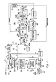
- FIGURE 1. illustrates a block diagram of a horizontal deflection circuit including a phase-lock-
loop circuit 20. It includes asequential counter 21 that has the analogous function of a VCO of a conventional phase-lock-loop circuit.Counter 21 is a programmable counter that is incremented after each leading edge of a clock pulse CK having a period t CK, illustrated in the timing diagram of FIGURE 4a. It counts up, from an initial value of, for example, 1, until it is reset to the initial value by a reset pulse RESET at aninput terminal 21a of FIGURE 1. Pulse RESET controls the number of clock CK periods tcKthat are included in a corresponding period, or sequence, N, ofcounter 21. Successions of sequences N produced bycounter 21 define a recurring sequence. Each word CT, at an output port 21 b ofcounter 21, supplies, in a given sequence N, the current count ofcounter 21. - Illustratively, a digital word herein is represented as a
base 2 number that includes an integer, a fraction or a combination of an integer and a fraction. A negative number is represented as a 2's complement number. - Horizontal sync pulses Hs having a period H - (1 H sync pulses Hs), are coupled, illustratively, from a
conventional sync separator 60 of a television receiver to aphase detector 202. When phase-lock--loop circuit 20 is phase-locked to sync pulses Hs, provided that they are accompanied by low level of noise, the leading edge of each pulse MS that is coupled tophase detector 202 occurs substantially coincidentally with the last clock CK edge that occurs before the center of the corresponding sync pulse Hs. Pulse MS is generated by adecoder 23 when a predetermined value of word CT is detected. Thus, the center of each sync pulse Hs occurs a variable fraction f of clock CK period tcK of FIGURE 4a after the leading edge of pulse MS of FIGURE 1. - Variable fraction f is contained in a 1 H skew word SK that is also coupled to
phase detector 202.Phase detector 202 generates a period length adjusting word LPFO. Word LPFO is combined, in a horizontalperiod length generator 33, with a constant word PR to produce a word DPW. Word PR, for example, equals thevalue 910 where 910xtCK is equal to the nominal, or free-running period, of phase-lock-loop circuit 20. Note that clock CK period tCK is equal to
- Word DPW contains the calculated estimate, or computed, binary value of the actual period H of pulses Hs in the form of an integer number M of clock CK period tcK and a fractional number k of clock CK period tcK. Word DPW ia coupled to a counter period and
skew words generator 201 that generates 1 H skew word SK and a period word PERIOD. Word PERIOD, that contains the number of clock CK cycles in a givencounter 21 period N, is coupled to acomparator 200 that compares the current value of words CT and PERIOD and generates pulse RESET when word CT = word PERIOD. Pulse RESET initializescounter 21 to contain word CT=1 1 simultaneously with the next clock CK edge that, thereby, defines the end time of the current sequence N ofcounter 21 and the beginning time of the next sequence N. - Words CT are coupled through a programmable time shifter or delay 42 to provide delayed words Ca. The delay of
programmable delay 42 is controlled by an external word NPW that is coupled from a source not shown in the FIGURES. A word CMa, defined to include words SK and Ca that provide the fraction and integer parts, respectively, of word CMa, is coupled to aprogrammable delay 203. A word CMao is defined as the state of word CMa in which word Ca = 0. Word CMao defines a periodic event eCMao having a period that is equal to an estimated value of the actual period H, in accordance with word DPW. Event eCMao occurs fxtCKcafter the leading edge of clock CK that causes word Ca to become zero, as described later on. Fraction f is the value contained in 1 H skew word SK. - Horizontal period length word DPW is coupled to a divide-by-2
unit 46 that divides the value of word DPW by thefactor 2 to produce word HDPW that is indicative of one-half the horizontal period length H. Word HDPW is coupled to the control port ofprogrammable delay 203 that delays event eCMao, defined by word CMao, by H/2 in accordance with the value ofdelay 203 control word HDPW. - A word CMb, the output word of
programmable delay 203 includes a skew word SKB and a word Cb, providing the fraction and integer parts, respectively, of word CMb. A word CMbo is defined as the state of word CMb in which word Cb = 0. Word CMbo defines a periodic event eCMbo that occurs in the calculated estimate center of the interval between each pair of successive events eCMao - Words CMa and CMb are coupled to
ports multiplexer 40. Multiplexer 40 couples, alternately, words CMa and CMb to input port 51 a of a programmable time shifter or delay 51 of a phase-control-loop circuit 120. Words CMI and CMP, at an output port 51c ofprogrammable delay 51, represent an integer and a fraction, respectively, of clock CK period tcK of FIGURE 4a. Words CMI are coupled to a horizontaldrive pulse generator 253 that generates, each time word CMI=0, a pulse PGP having a width w that is controlled by an external word WIDTH. Pulse PGP is coupled frompulse generator 253 to an input terminal 54a of agate delay 54.Gate delay 54 delays pulse PGP by a fraction q of clock CK period tCK of FIGURE 4a, having a length that is determined in accordance with the value of word CMP of FIGURE 1, to produce a 2fH rate signal HORDRIVE at anoutput terminal 54b ofgate delay 54. Signal HORDRIVE is also coupled to a flip-flop unit 55. Each pulse of signal HORDRIVE causes the toggling of a signal TOGGLE at an output terminal 55a of flip-flop unit 55. Signal TOGGLE is coupled to a select terminal 40c ofmultiplexer 40. Signal TOGGLE causes, in accordance with its logical state, the alternate coupling of words CMa and CMb, respectively, to input port 51a a ofprogrammable delay 51. Thus, the timings of the pulses of signal HORDRIVE are controlled, alternately, by the words inports multiplexer 40. - It should be understood that an arrangement similar to the arrangement of FIGURE 1 may be used for generating a signal analogous to signal HORDRIVE of Figure 1 having a different multiple of the frequency fH such as, illustratively, 3fHor 4f H.
- Signal HORDRIVE is coupled to an input terminal 41 a of a 2fHhorizontal deflection
circuit output stage 41 to control the switching of a horizontal output transistor. A retrace interval is formed in response to a corresponding pulse of signal HORDRIVE. A resulting pulse FLYBACK, occurring during retrace, that is obtained, illustratively, from a flyback transformer, not shown in FIGURE 1, ofoutput stage 41, is coupled to a phase detector 202'. - When phase-contral-
loop circuit 120 is perfectly phase-locked to flyback pulses FLYBACK, the leading edge of each pulse MS', that is also coupled to phase detector 202', occurs substantially coincidentally with the last clock CK edge before the center time of the respective pulse FLYBACK. Pulse MS' is generated by adecoder 23' when a predetermined value of word Ca is detected. The center of pulse FLYBACK occurs fraction f of clock CK period tεK of FIGURE 4a after the leading edge of pulse MS' of FIGURE 1. Fraction f is contained in 1 H skew word SK. - Phase detector 202' generates a word LPFO' that controls the delay time of
programmable delay 51.Programmable delay 51 is capable of providing a positive or negative phase shift, or time delay, as explained later on. The center of 2fH rate pulses FLYBACK occurs coincidentally with each corresponding event ecmaoor ecmbo. Event ecmaooccurs during the time in which word Ca = 0; whereas event eCMbooccurs when word Cb = 0, as described before. Therefore, the arrangement of FIGURE 1 generates the 2fH rate pulses FLYBACK, delayed by corresponding constant delay times relative to the corresponding 1 H sync pulse Hs. - FIGURE 2 illustrates a more detailed block diagram of the arrangement of FIGURE 1. Similar numerals and symbols in FIGURES 1 and 2 illustrate similar items or functions. FIGURES 4a-4r illustrate timing diagrams of a typical steady state example, showing three consecutive periods, or sequences, Na, N b and Nc of
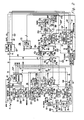
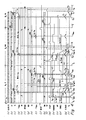
counter 21 of FIGURE 2, when phase-lock-loop circuit 20 is phase-locked to sync pulses Hsof FIGURE 4r. Similar numbers and symbols in FIGURES 1, 2 and 4a-4r represent similar items or functions. - Assume that word DPW, at an input port 34a of an
adder 34 of FIGURE 2, contains the calculated estimate value of period H of horizontal sync pulses Hsof FIGURE 4r. Word DPW of FIGURE 2 includes, illustratively, 10-bit number, M, representative of an integer multiple of clock CK periods tCKOf FIGURE 4a, and 5-bit number, k, representative of a fraction of period tCK. The value (M + k)-xtCK defines the updated estimate of period H. - Skew word SK, representing fraction f, at an output port 38b of a
latch 38 of FIGURE 2, is coupled, right justified, to aninput port 34b ofadder 34, where it is summed up with right justified word DPW. A word CNTPR appears at anoutput port 34c ofadder 34 to represent the integer part of the addition result. Each bit of word CNTPR is at the same numerical weight as the corresponding bit of the integer part, M, of word DPW. Word CNTPR is coupled to an input port 35a of alatch 35.Latch 35 stores the value of word CNTPR, at a time Ttof FIGURE 4f under the .control of a pulse CL ofdecoder 23 of FIGURE 2, to form period length word PERIOD at an input port 36a of asubtractor 36.Subtractor 36 controls the total number of states in a givencounter 21period N. Decoder 23 decodes counter 21 words CT and generates timing control signals such as pulse CL, as well as other timing pulses that are mentioned later on, when a corresponding predetermined state ofcounter 21 occurs. Pulse CL is also coupled to aclock input terminal 38a oflatch 38 for storing, at time Tt of FIGURE 4e, a word SKIN of FIGURE 2 to produce 1 H skew word SK that contains fraction f. The bits of fraction f appear at the same numerical scale, or weight, as the corresponding bits of fraction k of word DPW. Fraction f is representative of the fractional part of the addition result. Thus, adder 34 adds rightjustified latch 38 output word SK, that was formed by pulse CL during the immediately preceding period N ofcounter 21, to right justified word DPW, for updating words PERIOD and SK, respectively, at time Tt of FIGURES 4f and 4e, respectively. -
Counter 21 output word CT of FIGURE 2 is coupled to aninput port 36b ofsubtractor 36 where it is subtracted from word PERIOD to form, in a port 36c, a word RS. Word RS is coupled to a zerodetector 37. Zerodetector 37 issue pulse RESET, as illustrated in FIGURE 4j, when word RS of FIGURE 2 is equal to zero. Thus, when counter 21 word CT is equal to counter 21 period word PERIOD, counter 21 is reset and thenext counter 21 word CT is equal to 1, the initial counting state. Word PERIOD expresses, in multiples of clock CK periods tCKOf FIGURE 4a, the length of period N ofcounter 21 of FIGURE 2. - Word Ca, illustratively 10-bit wide, is obtained by subtracting, in a subtractor that represents
programmable delay 42 of FIGURE 1, the current word CT ofcounter 21 of FIGURE 2 from constant word NPW. FIGURE 4c illustrates an example of the corresponding sequence that is represented by words Ca. When word CT is equal to word NPW, word Ca is equal to 0. Similarly, when word CT exceeds word NPW by 1, word Ca is equal to 1023, in accordance with conventional 2's complement arithmetic. In each counter 21 sequence N, the states Ca=1, Ca=0 and Ca=1023 occur, respectively, ascounter 21 of FIGURE 2 is incremented sequentially. The time in which word Ca of FIGURE 4c becomes zero is defined as time tCTJ. Time tCTJoccurs (J-1) clock CK periods tCK after sequence N beginning time, such as time To of period Na. During clock CK period tcK that follows time To, counter 21 word CT is equal to 1. Word CMao is defined as the state of word CMa in which word CA=0, as described before. Each word CMao thus defines periodic event eCMaothat occurs at time tCMao = tCTJ+f xtCK, as illustrated by the corresponding short arrows in FIGURE 4d. Note that word SK of a given word CMao may have different values in correspondingcounter 21 periods N. For example, during the interval tCK that immediately follows time tCTJ of FIGURE 4e, word SK is equal to f,. Thus, event eCMao of FIGURE 4d occurs at time tCMao=tCTJ + f x tcK. Note that fraction f, was computed during period N ofcounter 21 of FIGURE 2, not shown in FIGURE 4a-4r, that occurred immediately prior to period Na. - The arrangement of FIGURE 2 computes the timing of the next event ecMao of FIGURE 4d, such as time tCMao' of event eCMao' relative to time tori, by adding, in
adder 34, old fraction f, of word SK of FIGURE 2, to fraction k of word DPW to produce new fraction f2. A binary carry C may be produced from such addition and the corresponding new period word PERIOD becomes (M+the value of carry C), at time Tt of FIGURE 4f. The interval between successive events ecMao of FIGURE 4d is equal to (M + k) x tcK, as shown by the examples below. - Assume, hypothetically, that prior to time Tt of FIGURE 4e the fractional result, word SKIN of FIGURE 2 = (f,+k), is <1; since no carry C is produced, word CNTPR is equal to M, the integer part of word DPW. After pulse CL of FIGURE 2 occurs, at time Tt of FIGURE 4e, word SK is equal to f2=(f,+k) and word PERIOD of FIGURE 4f is equal to M. Since reset pulse RESET of FIGURE 4j occurs when word CT of FIGURE 2 is equal to word PERIOD, the length of
counter 21 period Na is going to be equal to (M) clock CK periods tcK of FIGURE 4a. The corresponding event eCMao that occurs at time tcMao of FIGURE 4d duringcounter 21 period Na, occurs (J-1 +f,) x tCKafter beginning time To of period N of FIGURE 4b. - Assume, in a second hypothetical example, that prior to time Tt' of FIGURE 4e, the fractional result, word SKIN of FIGURE 2 = fz+k, is >1; consequently, carry C is produced in
adder 34, and word CNTPR of is equal to (M + 1). It follows that after pulse CL occurs, at time Tt' of FIGURE 4e, fraction f3, represented by word SK of FIGURE 4e, is equal to (f,+k)+k-1, and word PERIOD of FIGURE 4f is equal to (M + 1). Therefore, the length ofcounter 21 period Nb of FIGURE 4b is going to be equal to (M + 1) clock CK periods tcK. The corresponding event eCMao', duringcounter 21 period Nb, occurs (J-1 +f,+k) x tcKafter beginning time To' of period Nbof FIGURE 4b. - Assume, in a third hypothetical example, that prior to time Tt", the fractional result, word SKIN of FIGURE 2 = (f,+2k-1)+k, is <1; since no carry C is produced, word CNPTR is equal to M. It follows that after pulse CL occurs, at time Ti" of FIGURE 4e, the corresponding word PERIOD of FIGURE 4f is equal to M. Therefore, the length of
counter 21 period Nc of FIGURE 4b is going to be equal to - (M) clock CK periods tCK. The corresponding event e CMao" occurs (J-1+f1+2k-1)xtCKafter beginning time To" of period Nc of FIGURE 4b. - The above calculations lead to the conclusion that the interval t'cmao -tcMaoof FIGURE 4d, of successive events eCMao, is equal to :
- [To'-tCMao]+ [tCMao -To']= [M-(J-1+f1)]+ [J-1 + f, + k]-=(M+k) of clock CK periods tck. Likewise, the interval t"CMao-t'CMao is equal to :
- [To"-tCMao]+ [tCMao "-To"]= [(M + 1)-(J-1 + f, + k)] + [J-1 +f1+2k-1]=(M+K) of clock CK periods tck. Thus, the length of the interval between successive events ecMao of FIGURE 4d is expressed in the content, (M+k), of word DPW of FIGURE 2. The length of a given period N of FIGURE 4b may be, for example, either (M) or (M + 1) clock CK periods tcK; however, the average length of period N, is equal to period H of horizontal sync pulses H s of FIGURE 4r, as explained later on.
- At time t CH of FIGURE 4g, which occurs prior to time Tt of period Na, fraction f in
latch 38 of FIGURE 2 is saved in a latch 45 to form a word SKD. The saving of word SK is done by a pulse CH fromdecoder 23. Word SKD is.coupled, right adjusted, to aninput port 47b of anadder 47 that is similar toadder 34. Word DPW, that contains - (M + k), is coupled through divide-by-2unit 46 that includes, for example, a right shifter, to the other input port ofadder 47 to form there right adjusted word HDPW that is equal to (1/2) x (M + k). A word IHP, the integer part of the result of the addition inadder 47, is coupled to an input port 49a of anadder 49. Word Ca ofprogrammable delay 42 is coupled to aninput port 49b ofadder 49 where it is added with word IHP to form word Cb. Skew words SKB of FIGURES 4g and 2 contains a fractional part g of the result of the addition of the respective fractions inadder 47. - Word Cb is equal to 0 during the length of clock CK period tcK that immediately follows clock CK edge of a time tCTB of FIGURE 4h. Word CMbo of FIGURE 2 that is defined as the state of word CMb in which word Cb=0, is thus defined in an analogous manner to the way word CMao was defined before. Similarly to words CMao, words CMbo define corresponding periodic events eCMbo of FIGURE 4i, that are analogous to events eCMao of FIGURE 4d. In an analogous manner, event eCMbo of FIGURE 4i, for example, occurs g x tcK after time tCTB of FIGURE 4h.
- As explained before,
programmable delay 203 of FIGURE 1 that is controlled by word HDPW, delays the occurrence of event eCMao of FIGURE 4d by a duration that is determined in accordance with the value of word HDPW of FIGURE 2 to define event eCMbo of FIGURE 4i. Event e CMbo is delayed by H/2 relative to the corresponding event e CMao of FIGURE 4d. Each event eCMbo of FIGURE 4i occurs at the center of the corresponding interval that lies between consecutive events ecMao of FIGURE 4d, as shown by the example below. - During counter 21 period Na of FIGURE 4g, prior to time tcH, latch 45 of FIGURE 2 contains fraction f,. Since word HDPW is equal to (1/2) x - (M+k), the addition result at port 47c of
adder 47 is equal to (1/2)x(M+k)+f1. Assume, hypothetically, that M is an odd number that is equal to 2A + 1. The number A, an integer, is thus equal to
adder 49, word Cb of FIGURE 4h will be equal to zero when (A) clock CK periods tCKhave elapsed after time tCTJ of FIGURE 4c. Thus, event eCMbo of FIGURE 4i of time tCMbo occurs (A)xtCK+ - (1/2+k/2+f,) x tCK after time tCTJof FIGURE 4c. The total delay time, TH/2ain FIGURE 4i, from time tCTJ to the corresponding time tCMbo is equal to

- Each fH rate sync pulse Hs of FIGURE 2 is sampled by clock CK and the corresponding sample is digitized in a
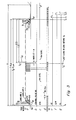
digitizer unit 61, such as an analog-to-digital converter, to form, in a conven- tional manner, acorresponding word 207. Successivedigitized sync words 207 are coupled to an input port 25a of a digitallow pass filter 25. Suc- ceessive digitized sync words SY, at the output offilter 25 are coupled to an input port 22a of async phase comparator 22. As described below, sync words SY are used for synchronizing each event ecmao of FIGURE 4d with the corresponding sync pulse Hs of FIGURE 4r, and for obtaining period length word DPW of FIGURE 2. - FIGURES 3a-3g illustrate schematically timing diagrams useful in explaining the synchronization of phase-lock-
loop circuit 20 of FIGURE 2. Similar symbols and numerals in FIGURES 2, 3a-3g, and 4a-4r illustrate similar items or functions. FIGURE 3a illustrates an example of successive digitized sync words SY of FIGURE 2 that result from digitizing an idealized trapezoidal horizontal sync pulse Hs, defining atrapezoidal envelope 1, during interval T of FIGURES 4r and 3a.Envelope 1 of FIGURE 3a has a leading edge 72 and a trailingedge 73, illustrated by dashed lines. During entire interval T, between times Tband Te, respectively, each sync word SY appears after each leading edge of clock CK of FIGURE 3d. Words SY are illustrated schematically by the vertical arrows that reach up toenvelope 1, representing the respective magnitude of words SY. -
Decoder 23 of FIGURE 2 produces control pulse MS at time Tm of FIGURE 3c or 41 when a predetermined value of word CT of FIGURE 2 occurs, such as, for example when word CT is equal to 315. Control pulse MS is coupled to a terminal 22b ofphase comparator 22 where it is phase-compared with a corresponding sync pulse Hs, that forms words SY, as described below. - Figure 5 illustrates schematically a block diagram of
phase comparator 22. Similar symbols and numerals in FIGURES 1, 2, 3a-3g, 4a-4r and 5 indicate similar items or functions.Phase comparator 22 of FIGURE 5 includes anaccumulator 26 that substractively accumulates, from an initial value of zero, successive sync words SY of FIGURE 3a from time T b, at the beginning of interval T of FIGURE 3a, as controlled by a signal CAC ofdecoder 23 of FIGURE 2, through time Tm of Figure 3a. At time Tm associated with pulse MS of Figure 5, a signal FFO at anoutput terminal 27a of a flip-flop 27, toggles from a first logical level to a second logical level, as illustrated in FIGURE 3c. Flip-flop 27 signal FFO of FIGURE 5 toggles after receiving, at aclock input terminal 22b, the leading edge of control pulse MS. After time Tm, and until interval T end time Teof FIGURE 3a, as controlled by signal CAC, individual sync words SY are additively accumulated inaccumulator 26 to provide an output word ACW that contains the total accumulation of the substractions and the subsequent additions. - In a second timing example of FIGURE 3a, sync words SY, referred to as sync words SY2, are illustrated schematically by vertical arrows that define an
envelope 2.Envelope 2, that is illustrated by the dotted lines, has a leading edge 70 and a trailing edge 71, that are similar to the respective edges inenvelope 1. Words SY2 are provided within an interval T2 that is equal in length to interval T. A center point Tc2 of interval T2 is delayed relative to center point Tc of interval T. Note that each word SY2 is of a smaller value at leading edge 70 but of a larger value at trailing edge 71 ofenvelope 2 than the corresponding words SY1 of leading edge 72 and trailingedge 73, respectively, ofenvelope 1. Therefore, the sum total in word ACW, at an end time Te2 of period T2, is more positive than at end of time Teof period T. Thus, the magnitude of word ACW is proportional to the length of the corresponding interval Tc2-Tmor Tc-Tm. It follows that the magnitude and polarity values of word ACW correspond with the time difference, (Tc-Tm), between actual center point Tc of interval T and time Tm that is defined by the leading edge of pulse MS of FIGURE 3b. - Output word ACW of
accumulator 26 of FIGURE 5 is coupled to aninput port 28a of ascaler 28.Scaler 28 generates from word ACW a word SCW that expresses the time difference, (Tc-Tm) of Figure 3a as a ratio n that is equal, illustratively, to (Tc-Tm )/tcK. Ratio n has a resolution of time difference (Tc-Tm), illustratively, of 1/32 of clock CK period tcK. - Word SK of FIGURE 2, that contains fraction f, is coupled to a
port 22d ofsubtractor 30 of FIGURE 5 where it is subtracted from word SCW to form a word SCWD at aninput port 22g of aregister 31.Register 31 stores each word SCWD and transfers it to anoutput port 22e to provide a phase word PH of FIGURE 5. Phase word PH, that is, consequently, equal to [(Tc-Tm)/tCK-f], is clocked into and out ofregister 31 by a pulse CC ofdecoder 23 of FIGURE 2 that is coupled to aclock terminal 22c at instant Tr of FIGURE 3e following end time Te of period T of FIGURE 3a. - A time Tcc = Tm+fxtCK, as described later on, represents the calculated, or expected, occurrence time of the center of period T of FIGURE 3a. The interval between time Too and the corresponding time tcMao of event eCMao is inherently equal to a predetermined integer multiple of clock CK periods tCK of FIGURE 3d. It follows that time Tocis also periodic with the same period length of (M + k) x t CK as time tCMao of event eCMeoof FIGURE 4d. Thus, in order to synchronize the occurrences of events eCMao to the corresponding sync pulses Hs of FIGURE 4r, it is sufficient that the actual center point Tc of period T of FIGURE 3a coincides with the calculated time Tcc. Word PH of FIGURE 2 that is equal to [(Tc-Tm)/tCK -f], is thus indicative of the time difference between the actual center point Tc, and the calculated center point Tcc of interval T of FIGURE 3a. When word PH of FIGURE 2 is positive, the actual center time Tc of FIGURE 3a is greater, or later, than the calculated center time Too. Conversely, when word PH of FIGURE 2 is negative, the actual center time Tc of FIGURE 3a is smaller, or earlier, than the calculated center time Tcc. When time Tcc is equal to time Tc, phase word PH of FIGURE 2 is zero.
- Phase word PH is coupled through a conventionally built digital
low pass filter 32 of Figure 2 to aninput port 33b of anadder 33 to formfilter 32 output word LPFO.Filter 32 may comprise an accumulator that additively accumulates individual phase words PH, under the control of a horizontal rate pulse CLPF generated bydecoder 23 at a corresponding time Ts of FIGURE 3f. Time Ts appears after time Trof pulse cc of FIGURE 3e. When phase word PH of FIGURE 2 is zero, in the steady state example, word LPFO oflow pass filter 32 does not change. A negative phase word PH, for example, decreases the value of word LPFO; whereas a positive phase word PH increases it. The adder ofgenerator 33 adds word PR that represents the nominal number of clock CK periods tCKcontained in a given period H of the NTSC composite television signal, to the integer part of word LPFO for forming deflection period word DPW atport 33a. As described before, period length word DPW is added with 1 H skew word SK to produce updated words PERIOD and SK when pulse CL occurs at time T, of FIGURE 3g. Time Tt occurs shortly after time Ts of FIGURE 3f. - Assume, hypothetically, that actual center time Tc of FIGURE 3a is later than calculated center time Tcc consequently, phase word PH of FIGURE 2 is a positive value. Word DPW becomes larger when phase word PH becomes more positive. In the subsequent interval T of FIGURE 3a, the larger word DPW produces calculated center time Tcc, representing a longer time interval from the previous time Tcc. Thus calculated center time Tccbecomes closer to actual center time Tcfor achieving synchronization. In a steady, or synchronized, state, clock CK edge of FIGURE 3d at time Tm, occurs a fraction of clock CK period tcK, that is equal to f, prior to actual center point Tc of interval T of FIGURE 3a. In the steady, or synchronized, state, each of events eCMao and e CMbo of FIGURES 4d and 4i, respectively, that are associated with words CMa and CMb, respectively, of FIGURE 2, occurs a corresponding constant delay time, respectively, from the corresponding horizontal sync pulses Hs of FIGURE 4r.
- When output signal TOGGLE, of flip-
flop unit 55 at select terminal 40c ofmultiplexer 40 of FIGURE 2, is at the first logical state, words CMa inport 40a are coupled right adjusted to input port 51 a ofprogrammable delay 51 that comprises an adder. Phase shifting word LPFO' of phase-control-loop circuit 120 is coupled, right adjusted, to port 51 b of the adder ofprogrammable delay 51. Word CMI at output port 51 c ofdelay 51, representing the integer part of the result of the addition inprogrammable delay 51, as illustrated - schematically in FIGURE 4k, is coupled to a zerodetector 52. Zerodetector 52 generates a pulse START at time TCMIO of FIGURE 4m, when word CMI of Figure 4k becomes zero. Pulse START of FIGURE 2 is coupled to pulse generator unit 53 causing it to generate, in a conventional manner, pulse PGP having a width w that is controlled by external controlling word WIDTH. Word WIDTH is coupled to an input port 53c of pulse generator 53. Pulse PGP is coupled togate delay 54 that delays each individual pulse PGP by a fraction q of clock CK period tCK, thus producing a corresponding individual pulse hd component of signal HORDRIVE of FIGURE 4n. Fraction q of word CMP at output port 51 c ofdelay 51 of FIGURE 2 represents the fractional part of the result of the summation at the adder ofprogrammable delay 51. The width w of pulse hd1 of FIGURE 4h is, illustrafively, wide enough to overlap the corresponding width of pulse fb1 of FIGURE 4q. -
Gate delay 54 may include a delay line of tCKtime delay, having, for example, 32 uniformly distributed taps. A given 5-bit combination of word CMP of FIGURE 2 may select a corresponding tap of the 32 taps for delaying pulse PGP a fraction of clock CK period tcK in accordance with its numerical value. For example, when fraction q of word CMP is equal to (00101)z, the delay obtained is equal to (5/32) xtCK. Thus, an individual component pulse hd1 of signal HORDRIVE of Figure 4n occurs, for example, at time(TCMIO+q,xtCK), where q, is the fraction contained in word CMP of FIGURE 2. - After, for example, the occurrence of the trailing edge of pulse hd1 component of signal HORDRIVE of FIGURE 4n, signal TOGGLE changes its state to be at a second state, as illustrated in FIGURE 4p. Now signal TOGGLE causes words CMb in
port 40b ofmultiplexer 40 of FIGURE 2 to be coupled to input port 51 a ofprogrammable delay 51 in the form of words CMI and CMP at its output port 51c. Zerodetector 52 now generates pulse START at time TCMIO' of FIGURE 4m, when word CMI of FIGURE 4k at port 51 c ofprogrammable delay 51 of FIGURE 2, becomes zero. This is done in a manner similar to that described before with respect to time TCMIO. Time TCMIO' of FIGURE 4m is thus determined now by words Cb of FIGURE 4h. The ensuing trailing edge of pulse hd2component of signal HORDRIVE of FIGURE 4n will causeflipflop unit 55 of FIGURE 2 to revert back to the first state, as illustrated in FIGURE 4p, for coupling, as explained before, words Ca and SK of each word CMa atport 40a to input port 51 a ofprogrammable delay 51 of FIGURE 2. Thus, in accordance with an aspect of the invention, the timings of alternate first and second component pulses hd of signal HORDRIVE of FIGURE 4n, are controlled, alternately, by words CMa and CMb inports multiplexer 40 of FIGURE 2. - Each pulse FLYBACK of
output stage 41 having illustratively, a trapezoidal shape, as illustrated in FIGURE 4q, and derived from horizontal flyback pulses, may be digitized in a digitizer unit 61', that is analogous todigitizer unit 61, to form successive digitized flyback words SY' at an input port 22a' of a phase comparator 22'. Flyback words SY' of phase-control-loop circuit 120 are analogous to sync words SY of phase-lock-loop circuit 20. Phase comparator 22' may be constructed similarly to phasecomparator 22 of phase-lock-loop circuit 20. Thus, ports 22a'-22e' of phase comparator 22' respectively, are functionally equivalent to ports 22a-22e, respectively, ofphase comparator 22. Adecoder 23' decodes corresponding predetermined values of words Ca for generating pulses MS' CAC', CC' and CLPF', respectively, that are analogous to pulses MS, CAC, CC and CLPF, respectively, ofdecoder 23. Pulse CC', for example, is coupled to terminal 22c'. Skew word SK is similarly coupled toport 22d' of phase comparator 22'. - Assume that flyback words SY', representing a trapezoidal envelope that is similar to
envelope 1 of sync words SY of FIGURE 3a, for example, are consecutively generated during a retrace interval T' of FIGURE 4q that has an actual center time Tc.' Interval T' and center time Te' are analogous to interval T and center point Tc of FIGURE 3a, respectively. In the example of FIGURE 4q, the leading edge of pulse MS' of FIGURE 2, that is coupled to terminal 22b' of phase comparator 22', occurs at time tCTJ of FIGURES 4d as illustrated in FIGURE 4o. In an analogous manner to the operation ofphase comparator 22, a phase word PH' atport 22e' of phase comparator 22'of FIGURE 2 is indicative of the corresponding time difference (Tc'- tCMao). The term tcMao in phase word PH', is analogous to the term T cc in phase word PH ofphase comparator 22. Using the same analogy, it follows that when center point Tc' of interval T' of an individual pulse fb1 of pulses FLYBACK of FIGURE 4q is greater than the corresponding time tCMao of FIGURE 4d, phase word PH'of FIGURE 2 is positive. On the other hand, when time Tc' of FIGURE 4q is equal to time tcMao, phase word PH' of FIGURE 2 is zero. - Phase word PH' of FIGURE 2 is coupled to a
sign complementing unit 58 that provides a sign complemented word PHi. When word PH' is negative, for example, word PHi is positive and of, illustratively, the same absolute value as word PH'. Words PHi are coupled to a low pass digital filter 32' that is analogous to filter 32 of phase-lock-loop circuit 20. Filter 32' output word LPFO' has a shorter response time to phase variations of pulses FLYBACK of FIGURE 4q than the response time oflow pass filter 32 to phase variations of pulses Hs of FIGURE 4r. In the steady state of phase-control-loop circuit 120 of FIGURE 2, occurring when phase word PH' is zero, word LPFO' is negative with such a value that causes center point Tc', of alternate flyback pulses fb1and fb3 pulses FLYBACK of FIGURE 4q, to occur at times tCMao and, tCMao, respectively, of FIGURE 4d. It can be shown that component pulse hdi, for example, of signal HORDRIVE of FIGURE 4n, occurs prior to the corresponding time tCMaoof FIGURE 4d by a period tLEAD that is equal to (Q + h) xtCK, where Q and h are the integer and fractional parts respectively, of word LPFO' of Figure 2. - Word NPW of FIGURE 2, that is coupled to the adder of
programmable delay 42, controls the relative timing between pulse MS' ofdecoder 23' and the corresponding pulse MS ofdecoder 23. By changing the value of word NPW a corresponding change of the duration between, for example, center times Tc' and Tcof pulses fb1 and Hsa of FIGURES 4q and 4r, respectively, is obtained. - As a result of a beam current change in the picture tube, the ultor current changes. The change in ultor current drawn from to the flyback transformer of
output stage 41 causes the delay between pulse fb1of FIGURE 4q and pulse hd1 of FIGURE 4n also to change because of the change in storage time of the horizontal output switching transistor. Assume that as a result of such change in delay, the interval (Tc'-tCMao) of pulse fb1 of FIGURE 4q deviates from zero and becomes positive. In this case, word PH' of FIGURE 1 becomes more positive and word LPFO' becomes more negative. Therefore, the next pulse hd3 of FIGURE 4n occurs earlier, causing pulse f b3 of pulses FLYBACK of FIGURE 4q to occur earlier. This leads to a decrease in the length of the subsequent interval (Tc'-t CMao') so as to correct for the assumed deviation caused by the corresponding beam current change. - In accordance with an aspect of the invention, the same value of word LPFO' of FIGURE 2 controls the timings of successive pulses hd of FIGURE 4n that correspond with events ecMao and eCMbo, respectively. Because, for example, time tCMbo of FIGURE 4i is spaced from time tcMao of FIGURE 4d by a period length of H/2, as shown in FIGURE 4q and as described before, pulse fb2 of flyback pulses FLYBACK of FIGURE 4q that corresponds with time tCMbo of FIGURE 4i, appears H/2 after the immediately preceding pulse fb1of pulses FLYBACK of FIGURE 4q. Pulse fbicorresponds with time tCMaoof FIGURE 4d. Thus, updating low pass filter 32' by pulse CLPF' of FIGURE 2 occurs once in each horizontal period H. It should be understood that
decoder 23' may be designed so that updating low pass filter 32' occurs at a rate of, illustratively, 2fHthat corresponds with the rate of flyback pulses FLYBACK of FIGURE 2q. - When sync pulses Hs of FIGURE 2 are absent, causing word LPFO of
filter 32 to be zero, word DPW, which is equal to word PR=910, causes the arrangement of FIGURE 1 to form retrace intervals separated by 910/2 X tcK, that is equal to 1/2 the nominal value of period H in an NTSC system.
Claims (9)
Priority Applications (1)
| Application Number | Priority Date | Filing Date | Title |
|---|---|---|---|
| AT86302179T ATE95020T1 (en) | 1985-04-01 | 1986-03-25 | LINE DEFLECTION ARRANGEMENT. |
Applications Claiming Priority (2)
| Application Number | Priority Date | Filing Date | Title |
|---|---|---|---|
| US06/718,300 US4636861A (en) | 1985-04-01 | 1985-04-01 | Two-loop line deflection system |
| US718300 | 1985-04-01 |
Publications (3)
| Publication Number | Publication Date |
|---|---|
| EP0200348A2 true EP0200348A2 (en) | 1986-11-05 |
| EP0200348A3 EP0200348A3 (en) | 1988-05-04 |
| EP0200348B1 EP0200348B1 (en) | 1993-09-22 |
Family
ID=24885593
Family Applications (1)
| Application Number | Title | Priority Date | Filing Date |
|---|---|---|---|
| EP86302179A Expired - Lifetime EP0200348B1 (en) | 1985-04-01 | 1986-03-25 | Line deflection system |
Country Status (10)
| Country | Link |
|---|---|
| US (1) | US4636861A (en) |
| EP (1) | EP0200348B1 (en) |
| JP (3) | JP2607066B2 (en) |
| KR (1) | KR920003164B1 (en) |
| AT (1) | ATE95020T1 (en) |
| CA (1) | CA1256980A (en) |
| DE (1) | DE3689051T2 (en) |
| ES (1) | ES8707835A1 (en) |
| FI (1) | FI79921C (en) |
| HK (1) | HK1004051A1 (en) |
Cited By (2)
| Publication number | Priority date | Publication date | Assignee | Title |
|---|---|---|---|---|
| WO1991015081A1 (en) * | 1990-03-26 | 1991-10-03 | Thomson Consumer Electronics, Inc. | Display locked timing signals for video processing |
| EP0479142A2 (en) * | 1990-10-03 | 1992-04-08 | Thomson Consumer Electronics, Inc. | Synchronizing circuit |
Families Citing this family (11)
| Publication number | Priority date | Publication date | Assignee | Title |
|---|---|---|---|---|
| EP0254763B1 (en) * | 1986-07-31 | 1991-01-23 | Deutsche ITT Industries GmbH | Digital horizontal-deflection circuit |
| US4775890A (en) * | 1987-06-11 | 1988-10-04 | Rca Licensing Corporation | Phase detector |
| JPH0793709B2 (en) * | 1987-09-30 | 1995-10-09 | 株式会社日立製作所 | Television receiver |
| US5223931A (en) * | 1990-03-26 | 1993-06-29 | Thomson Consumer Electronics, Inc. | Synchronized scanning at horizontal frequency |
| US5329367A (en) * | 1990-03-26 | 1994-07-12 | Thomson Consumer Electronics, Inc. | Horizontal blanking |
| KR930011431B1 (en) * | 1991-01-31 | 1993-12-06 | 삼성전자 주식회사 | Corresponding signal reproducing circuit for standard video signal |
| RU2215372C2 (en) * | 1991-03-25 | 2003-10-27 | Томсон Конзьюмер Электроникс, Инк. | Horizontal deflection yoke |
| JPH05207327A (en) * | 1992-01-27 | 1993-08-13 | Mitsubishi Electric Corp | Horizontal synchronizing circuit |
| US5677737A (en) * | 1995-12-27 | 1997-10-14 | Rca Thomson Licensing Corporation | Video compression for wide screen television |
| WO2004023390A1 (en) | 2002-08-30 | 2004-03-18 | Fujitsu Limited | Electronic storage apparatus, authentication apparatus, and authentication method |
| JP4158626B2 (en) | 2003-06-30 | 2008-10-01 | ソニー株式会社 | External storage device |
Citations (3)
| Publication number | Priority date | Publication date | Assignee | Title |
|---|---|---|---|---|
| US4317133A (en) * | 1980-09-29 | 1982-02-23 | Rca Corporation | Two-loop horizontal AFPC system |
| US4351001A (en) * | 1980-12-29 | 1982-09-21 | Motorola, Inc. | Horizontal phase lock loop for television |
| JPS57190462A (en) * | 1981-05-19 | 1982-11-24 | Hitachi Ltd | Horizontal deflecting circuit |
Family Cites Families (9)
| Publication number | Priority date | Publication date | Assignee | Title |
|---|---|---|---|---|
| US4031068A (en) * | 1976-07-26 | 1977-06-21 | Uniroyal Inc. | Non-migratory sulfonyl azide antioxidants |
| JPS5354953A (en) * | 1976-10-29 | 1978-05-18 | Hitachi Ltd | Frequency step-multiplication circuit |
| US4327376A (en) * | 1978-10-05 | 1982-04-27 | Rca Corporation | Dual phase-control loop horizontal deflection synchronizing circuit |
| US4292654A (en) * | 1979-12-20 | 1981-09-29 | Rca Corporation | Deflection system and switched-mode power supply using a common ramp generator |
| JPS6051312B2 (en) * | 1981-03-20 | 1985-11-13 | 日本ビクター株式会社 | Horizontal scanning frequency multiplier circuit |
| JPS5881386A (en) * | 1981-11-10 | 1983-05-16 | Sony Corp | Television receiver |
| JPS58154970A (en) * | 1982-03-10 | 1983-09-14 | Matsushita Electric Ind Co Ltd | Television receiver |
| US4467359A (en) * | 1982-04-15 | 1984-08-21 | Sanyo Electric Co., Ltd. | Horizontal synchronizing circuit |
| US4591910A (en) * | 1984-03-14 | 1986-05-27 | Zenith Electronics Corporation | Horizontal picture centering |
-
1985
- 1985-04-01 US US06/718,300 patent/US4636861A/en not_active Expired - Lifetime
-
1986
- 1986-03-25 ES ES553367A patent/ES8707835A1/en not_active Expired
- 1986-03-25 EP EP86302179A patent/EP0200348B1/en not_active Expired - Lifetime
- 1986-03-25 AT AT86302179T patent/ATE95020T1/en not_active IP Right Cessation
- 1986-03-25 FI FI861268A patent/FI79921C/en not_active IP Right Cessation
- 1986-03-25 DE DE86302179T patent/DE3689051T2/en not_active Expired - Lifetime
- 1986-04-01 CA CA000505563A patent/CA1256980A/en not_active Expired
- 1986-04-01 JP JP61076435A patent/JP2607066B2/en not_active Expired - Lifetime
- 1986-04-01 KR KR1019860002461A patent/KR920003164B1/en not_active IP Right Cessation
-
1993
- 1993-11-04 JP JP5301238A patent/JP3060424B2/en not_active Expired - Lifetime
-
1998
- 1998-04-14 HK HK98103037A patent/HK1004051A1/en not_active IP Right Cessation
-
2000
- 2000-02-18 JP JP2000041615A patent/JP3400968B2/en not_active Expired - Lifetime
Patent Citations (3)
| Publication number | Priority date | Publication date | Assignee | Title |
|---|---|---|---|---|
| US4317133A (en) * | 1980-09-29 | 1982-02-23 | Rca Corporation | Two-loop horizontal AFPC system |
| US4351001A (en) * | 1980-12-29 | 1982-09-21 | Motorola, Inc. | Horizontal phase lock loop for television |
| JPS57190462A (en) * | 1981-05-19 | 1982-11-24 | Hitachi Ltd | Horizontal deflecting circuit |
Non-Patent Citations (1)
| Title |
|---|
| PATENT ABSTRACTS OF JAPAN, vol. 7, no. 40 (E-159)[1185], 17th February 1983; & JP-A-57 190 462 (HITACHI SEISAKUSHO K.K.) 24-11-1982 * |
Cited By (6)
| Publication number | Priority date | Publication date | Assignee | Title |
|---|---|---|---|---|
| WO1991015081A1 (en) * | 1990-03-26 | 1991-10-03 | Thomson Consumer Electronics, Inc. | Display locked timing signals for video processing |
| TR25570A (en) * | 1990-03-26 | 1993-07-01 | Thomson Cons Electr Inc | VIEWO LOCKING TIMER SIGNALS FOR VIDEO PROCESSING. |
| EP0479142A2 (en) * | 1990-10-03 | 1992-04-08 | Thomson Consumer Electronics, Inc. | Synchronizing circuit |
| EP0479142A3 (en) * | 1990-10-03 | 1992-05-27 | Thomson Consumer Electronics, Inc. | Synchronizing circuit |
| US5162910A (en) * | 1990-10-03 | 1992-11-10 | Thomson Consumer Electronics, Inc. | Synchronizing circuit |
| TR28000A (en) * | 1990-10-03 | 1995-11-07 | Thomson Consumer Electronics | Digital synchronization circuit utilizing the counting tool. |
Also Published As
| Publication number | Publication date |
|---|---|
| FI79921B (en) | 1989-11-30 |
| KR920003164B1 (en) | 1992-04-20 |
| ES8707835A1 (en) | 1987-08-16 |
| HK1004051A1 (en) | 1998-11-13 |
| KR860008672A (en) | 1986-11-17 |
| JP3400968B2 (en) | 2003-04-28 |
| FI861268A0 (en) | 1986-03-25 |
| CA1256980A (en) | 1989-07-04 |
| FI861268A (en) | 1986-10-02 |
| JPS61230473A (en) | 1986-10-14 |
| AU5520586A (en) | 1986-10-09 |
| JP3060424B2 (en) | 2000-07-10 |
| US4636861A (en) | 1987-01-13 |
| EP0200348B1 (en) | 1993-09-22 |
| ES553367A0 (en) | 1987-08-16 |
| JPH0774977A (en) | 1995-03-17 |
| JP2607066B2 (en) | 1997-05-07 |
| JP2000224431A (en) | 2000-08-11 |
| DE3689051D1 (en) | 1993-10-28 |
| FI79921C (en) | 1990-03-12 |
| ATE95020T1 (en) | 1993-10-15 |
| AU589411B2 (en) | 1989-10-12 |
| DE3689051T2 (en) | 1994-04-28 |
| EP0200348A3 (en) | 1988-05-04 |
Similar Documents
| Publication | Publication Date | Title |
|---|---|---|
| EP0197699B1 (en) | Television sychronizing apparatus | |
| US5335074A (en) | Phase locked loop synchronizer for a resampling system having incompatible input and output sample rates | |
| US4636861A (en) | Two-loop line deflection system | |
| EP0189319A2 (en) | Phase-locked loop | |
| US6385267B1 (en) | System and method for locking disparate video formats | |
| US5043813A (en) | Display locked timing signals for video processing | |
| EP0126586B1 (en) | Television frame signal synchronizing circuits | |
| JPH0832836A (en) | Automatic frequency controller | |
| KR920009012B1 (en) | Circuit for controlling automatic frequency | |
| US5565928A (en) | Circuit for generating a scan at a multiple of a synchronizing signal | |
| US6597403B1 (en) | System for generating horizontal synchronizing signal compatible with multi-scan | |
| EP0328207A1 (en) | Color television signal decoding circuit | |
| KR940009585B1 (en) | Control signal generating circuit of time-base error compensation apparatus | |
| JP2644045B2 (en) | Time compression device for HDTV receiver | |
| JPS63220677A (en) | Horizontal driving signal generating circuit | |
| MXPA95002546A (en) | Synchronized exploration circuit | |
| JPS59149465A (en) | Vertical synchronizing circuit | |
| JPH0993545A (en) | Phase reference detector | |
| JPH07105897B2 (en) | Vertical sync signal generation circuit |
Legal Events
| Date | Code | Title | Description |
|---|---|---|---|
| PUAI | Public reference made under article 153(3) epc to a published international application that has entered the european phase |
Free format text: ORIGINAL CODE: 0009012 |
|
| AK | Designated contracting states |
Kind code of ref document: A2 Designated state(s): AT DE FR GB IT |
|
| PUAB | Information related to the publication of an a document modified or deleted |
Free format text: ORIGINAL CODE: 0009199EPPU |
|
| RA1 | Application published (corrected) |
Date of ref document: 19861210 Kind code of ref document: A2 |
|
| PUAL | Search report despatched |
Free format text: ORIGINAL CODE: 0009013 |
|
| AK | Designated contracting states |
Kind code of ref document: A3 Designated state(s): AT DE FR GB IT |
|
| RAP1 | Party data changed (applicant data changed or rights of an application transferred) |
Owner name: RCA LICENSING CORPORATION |
|
| 17P | Request for examination filed |
Effective date: 19881011 |
|
| 17Q | First examination report despatched |
Effective date: 19910924 |
|
| RAP1 | Party data changed (applicant data changed or rights of an application transferred) |
Owner name: RCA THOMSON LICENSING CORPORATION |
|
| GRAA | (expected) grant |
Free format text: ORIGINAL CODE: 0009210 |
|
| AK | Designated contracting states |
Kind code of ref document: B1 Designated state(s): AT DE FR GB IT |
|
| REF | Corresponds to: |
Ref document number: 95020 Country of ref document: AT Date of ref document: 19931015 Kind code of ref document: T |
|
| ITF | It: translation for a ep patent filed |
Owner name: ING. C. GREGORJ S.P.A. |
|
| REF | Corresponds to: |
Ref document number: 3689051 Country of ref document: DE Date of ref document: 19931028 |
|
| ET | Fr: translation filed | ||
| PLBE | No opposition filed within time limit |
Free format text: ORIGINAL CODE: 0009261 |
|
| STAA | Information on the status of an ep patent application or granted ep patent |
Free format text: STATUS: NO OPPOSITION FILED WITHIN TIME LIMIT |
|
| 26N | No opposition filed | ||
| PGFP | Annual fee paid to national office [announced via postgrant information from national office to epo] |
Ref country code: AT Payment date: 19990517 Year of fee payment: 14 |
|
| PG25 | Lapsed in a contracting state [announced via postgrant information from national office to epo] |
Ref country code: AT Free format text: LAPSE BECAUSE OF NON-PAYMENT OF DUE FEES Effective date: 20000325 |
|
| REG | Reference to a national code |
Ref country code: GB Ref legal event code: 732E |
|
| REG | Reference to a national code |
Ref country code: GB Ref legal event code: IF02 |
|
| PGFP | Annual fee paid to national office [announced via postgrant information from national office to epo] |
Ref country code: GB Payment date: 20050126 Year of fee payment: 20 |
|
| PGFP | Annual fee paid to national office [announced via postgrant information from national office to epo] |
Ref country code: DE Payment date: 20050318 Year of fee payment: 20 |
|
| PGFP | Annual fee paid to national office [announced via postgrant information from national office to epo] |
Ref country code: FR Payment date: 20050323 Year of fee payment: 20 |
|
| PGFP | Annual fee paid to national office [announced via postgrant information from national office to epo] |
Ref country code: IT Payment date: 20050324 Year of fee payment: 20 |
|
| PG25 | Lapsed in a contracting state [announced via postgrant information from national office to epo] |
Ref country code: GB Free format text: LAPSE BECAUSE OF EXPIRATION OF PROTECTION Effective date: 20060324 |
|
| REG | Reference to a national code |
Ref country code: GB Ref legal event code: PE20 |