EP0197516B1 - Méthode pour la production d'appareils électroniques - Google Patents
Méthode pour la production d'appareils électroniques Download PDFInfo
- Publication number
- EP0197516B1 EP0197516B1 EP86104569A EP86104569A EP0197516B1 EP 0197516 B1 EP0197516 B1 EP 0197516B1 EP 86104569 A EP86104569 A EP 86104569A EP 86104569 A EP86104569 A EP 86104569A EP 0197516 B1 EP0197516 B1 EP 0197516B1
- Authority
- EP
- European Patent Office
- Prior art keywords
- folding
- conductor foil
- casing
- plastic
- sections
- Prior art date
- Legal status (The legal status is an assumption and is not a legal conclusion. Google has not performed a legal analysis and makes no representation as to the accuracy of the status listed.)
- Expired - Lifetime
Links
Images



Classifications
-
- H—ELECTRICITY
- H05—ELECTRIC TECHNIQUES NOT OTHERWISE PROVIDED FOR
- H05K—PRINTED CIRCUITS; CASINGS OR CONSTRUCTIONAL DETAILS OF ELECTRIC APPARATUS; MANUFACTURE OF ASSEMBLAGES OF ELECTRICAL COMPONENTS
- H05K7/00—Constructional details common to different types of electric apparatus
- H05K7/14—Mounting supporting structure in casing or on frame or rack
- H05K7/1417—Mounting supporting structure in casing or on frame or rack having securing means for mounting boards, plates or wiring boards
-
- H—ELECTRICITY
- H05—ELECTRIC TECHNIQUES NOT OTHERWISE PROVIDED FOR
- H05K—PRINTED CIRCUITS; CASINGS OR CONSTRUCTIONAL DETAILS OF ELECTRIC APPARATUS; MANUFACTURE OF ASSEMBLAGES OF ELECTRICAL COMPONENTS
- H05K3/00—Apparatus or processes for manufacturing printed circuits
- H05K3/22—Secondary treatment of printed circuits
- H05K3/28—Applying non-metallic protective coatings
- H05K3/284—Applying non-metallic protective coatings for encapsulating mounted components
-
- H—ELECTRICITY
- H05—ELECTRIC TECHNIQUES NOT OTHERWISE PROVIDED FOR
- H05K—PRINTED CIRCUITS; CASINGS OR CONSTRUCTIONAL DETAILS OF ELECTRIC APPARATUS; MANUFACTURE OF ASSEMBLAGES OF ELECTRICAL COMPONENTS
- H05K1/00—Printed circuits
- H05K1/02—Details
- H05K1/03—Use of materials for the substrate
- H05K1/0393—Flexible materials
-
- H—ELECTRICITY
- H05—ELECTRIC TECHNIQUES NOT OTHERWISE PROVIDED FOR
- H05K—PRINTED CIRCUITS; CASINGS OR CONSTRUCTIONAL DETAILS OF ELECTRIC APPARATUS; MANUFACTURE OF ASSEMBLAGES OF ELECTRICAL COMPONENTS
- H05K1/00—Printed circuits
- H05K1/02—Details
- H05K1/09—Use of materials for the conductive, e.g. metallic pattern
- H05K1/092—Dispersed materials, e.g. conductive pastes or inks
-
- H—ELECTRICITY
- H05—ELECTRIC TECHNIQUES NOT OTHERWISE PROVIDED FOR
- H05K—PRINTED CIRCUITS; CASINGS OR CONSTRUCTIONAL DETAILS OF ELECTRIC APPARATUS; MANUFACTURE OF ASSEMBLAGES OF ELECTRICAL COMPONENTS
- H05K1/00—Printed circuits
- H05K1/18—Printed circuits structurally associated with non-printed electric components
- H05K1/189—Printed circuits structurally associated with non-printed electric components characterised by the use of flexible or folded printed circuits
-
- H—ELECTRICITY
- H05—ELECTRIC TECHNIQUES NOT OTHERWISE PROVIDED FOR
- H05K—PRINTED CIRCUITS; CASINGS OR CONSTRUCTIONAL DETAILS OF ELECTRIC APPARATUS; MANUFACTURE OF ASSEMBLAGES OF ELECTRICAL COMPONENTS
- H05K2203/00—Indexing scheme relating to apparatus or processes for manufacturing printed circuits covered by H05K3/00
- H05K2203/13—Moulding and encapsulation; Deposition techniques; Protective layers
- H05K2203/1305—Moulding and encapsulation
- H05K2203/1316—Moulded encapsulation of mounted components
-
- Y—GENERAL TAGGING OF NEW TECHNOLOGICAL DEVELOPMENTS; GENERAL TAGGING OF CROSS-SECTIONAL TECHNOLOGIES SPANNING OVER SEVERAL SECTIONS OF THE IPC; TECHNICAL SUBJECTS COVERED BY FORMER USPC CROSS-REFERENCE ART COLLECTIONS [XRACs] AND DIGESTS
- Y10—TECHNICAL SUBJECTS COVERED BY FORMER USPC
- Y10T—TECHNICAL SUBJECTS COVERED BY FORMER US CLASSIFICATION
- Y10T29/00—Metal working
- Y10T29/49—Method of mechanical manufacture
- Y10T29/49002—Electrical device making
- Y10T29/49117—Conductor or circuit manufacturing
- Y10T29/49124—On flat or curved insulated base, e.g., printed circuit, etc.
- Y10T29/4913—Assembling to base an electrical component, e.g., capacitor, etc.
- Y10T29/49133—Assembling to base an electrical component, e.g., capacitor, etc. with component orienting
- Y10T29/49137—Different components
-
- Y—GENERAL TAGGING OF NEW TECHNOLOGICAL DEVELOPMENTS; GENERAL TAGGING OF CROSS-SECTIONAL TECHNOLOGIES SPANNING OVER SEVERAL SECTIONS OF THE IPC; TECHNICAL SUBJECTS COVERED BY FORMER USPC CROSS-REFERENCE ART COLLECTIONS [XRACs] AND DIGESTS
- Y10—TECHNICAL SUBJECTS COVERED BY FORMER USPC
- Y10T—TECHNICAL SUBJECTS COVERED BY FORMER US CLASSIFICATION
- Y10T29/00—Metal working
- Y10T29/49—Method of mechanical manufacture
- Y10T29/49002—Electrical device making
- Y10T29/49117—Conductor or circuit manufacturing
- Y10T29/49124—On flat or curved insulated base, e.g., printed circuit, etc.
- Y10T29/4913—Assembling to base an electrical component, e.g., capacitor, etc.
- Y10T29/49146—Assembling to base an electrical component, e.g., capacitor, etc. with encapsulating, e.g., potting, etc.
Definitions
- the invention relates to a method for the production of electronic devices, in which a flexible conductor film provided with the etched circuit is folded after being fitted with the electronic components at predetermined folding sections for adaptation to the device shape, and this circuit unit is integrated into an image depicting the geometric device shape Forming tool is inserted and coated with a plastic, hardening plastic to form a housing body and then the hardened housing body consisting of sections from the individual folds is detached along a tear-out perforation.
- foldable flexible conductor foils Compared to the use of rigid printed circuit boards, foldable flexible conductor foils have the advantage that one can subdivide the folded flat circuit board into a large flat surface by folding and reduce it as desired by superimposing the folding sections.
- the object of the invention is to simplify the removal of the assembled and soldered foil circuit from the flexible conductor foil strip and the folding as well as the insertion of the circuit in the envelope mold and the fixing of the circuit in the mold itself.
- the housing body formed from the plastic, curable plastic is divided into housing parts so that these housing parts can be inserted into one another when the conductor foil is folded to form the closed housing body, the possibility is created in the area of each folding section embedded electronic components for themselves before folding into individual plastic molded parts and thus to form the housing parts.
- the housing sections are applied as individual plastic moldings to the folded sections of the flat, still unfolded conductor film, so that even before folding, the components, the soldering and the film itself result in protective folding pieces that can be easily done without special care and dexterity Way along a tear-off perforation, which is the one consisting of the individual folding sections Encloses the housing body and forms the outer contour of the overall circuit, detach it and let it fold into the closed housing on the flexible folding strips.
- the application of the housing sections can be automated by the features of claim 2, so that manual intervention is no longer necessary.
- a particularly expedient subdivision of the housing body results from the features of method claim 3, since the soldering sides of the folded sections which come into contact with one another are not only sufficiently stiffened and protected by the intermediate insulating layers, but are also securely protected against unwanted electrically conductive contact.
- the special insulation separating foils inserted up to now can be omitted. While the insulating intermediate layers can be made relatively thin in order to achieve space-saving folding, the housing sections surrounding the components are relatively thick-walled in that they simultaneously form the outer contours of the housing body, so that even larger components can be fully embedded before folding and thus protected.
- a plastic foam, in particular polyurethane foam, is expediently used as the plastic, curable plastic, which is only filled into one of the two mold halves and spreads through the openings in the conductor foil into the other mold half.
- the plastic foam envelops
- the components are particularly gentle due to their softness without exerting a pushing pressure on the perforated conductor foil and the components when filling the mold cavities.
- the opposite, jointly shaped housing sections are also directly connected to one another via the passage openings, so that a special adhesive effect between the conductor foil and plastic is not absolutely necessary.
- the housing sections with the embedded circuit folding sections are precisely fixed to each other when folded together without additional measures and at the same time securely connected to one another to form a closed housing body.
- a tension-free, easy folding of the plastic-covered folding sections can be achieved according to the housing body according to claim 6 by leaving a folding strip free between the adjacent plastic housing sections, the width of which is adapted to the height of the intermediate insulating layers after folding.
- the folding sections of the conductor foil can be in a sandwich construction, easily fold it into an electronic module that can be used directly in practice.
- housing sections from the assembly side of the conductor foil are provided with molded recesses into which folding sections with smaller housing sections can be folded, a component can be fitted in any desired end position regardless of the assembly of the plane tensioned conductor membrane perpendicular to the assembly level be tilted.
- folding sections which are to be inserted with their applied plastic housing part offset in the housing body regardless of a folding edge, are connected according to the feature of claim 9 via free tongue-like connecting webs of the conductor foil with the rest of the circuit on the conductor foil, they can be completely Arrange freely in any desired position and position.
- the assembled housing body can also be inserted into a prefabricated outer housing, which is closed by a cover at the insertion opening, so that a cheap plastic injection housing or a metal deep-drawn housing can be used.
- the housing sections can be applied with the molding tool according to claim 12 in a particularly simple manner on the still flat but equipped conductor foil in that the falling sections on the folding strips and on the edge strips formed by a tear-off perforation are tightly clamped between webs of the mold halves, whereby the individual Folded sections are firmly locked in the shape and the housing sections receive an exact and clean border.
- the recesses in the mold halves on the assembly side and the soldering side of the conductor foil are precisely adapted to the spatial contours required for the individual folding sections, so that when the mold cavities are filled with plastic curable plastic, all the components maintain their defined position exactly and when the plastic hardens in them , they are enveloping plastic, integrated.
- the mold halves for all folding sections are combined into a common lower and upper overall mold half, all housing sections can be produced in a simple manner with one mold.
- the electrical circuit consisting of the electronic components 2 and the etched conductor tracks 3 is applied to the conductor foil 1 shown in FIG. 1.
- This known flexible circuit is provided to divide the individual folding sections 4 with folding strips 5, which are marked by perforations 6, in order to facilitate the folding of the conductor foil 1.
- the outer edge of the circuit is formed by the tear-off perforation 7.
- the still unfolded flat conductor foil 1, which is equipped with the components 2, is clamped tightly between the lower mold half 10 and the upper mold half 11.
- the conductor foil 1 carries the circuit formed from the folding sections 4, between which the folding strips 5 with the two folding perforations 6 are provided.
- the outer boundary of the circuit is formed by the tear-off perforation 7.
- the housing body of the electronic device is divided into the housing sections 12, 13, 14 and 15, which can be inserted into one another when the circuit is folded to form the closed housing body.
- the lower mold half 10 is provided with depressions 16 which form the intermediate insulating layers 13 and 15.
- the upper mold half 11 carries in the area of the two folding sections 4 semi-cylindrical recesses 17 which form the half-cylinder sections 12 and 14 adapted to the outer contour of the housing body, which together form a cylindrical housing.
- the mold halves 10 and 11 are partially drawn in a raised position after curing of the plastic for better understanding.
- pins 18 are formed on the intermediate insulating layer 13 by means of shaped holes 19 which engage in snap holes formed by the pins 20 of the lower mold half 10.
- a polyurethane foam 21 is provided here as plastic, which encloses the components 2 in a particularly protective manner.
- the assembled conductor foil 1 has 38 centering holes 39 in the edge strips and the mold half 10 is provided with centering pins 40 which engage in corresponding bores in the other housing mold half 11.
- the mold halves 10 and 11 In order for the mold halves 10 and 11 to rest tightly on the folding strip 5 and the edge strip 38 of the conductor foil 1, the mold halves have inner webs 41 and edge webs 42.
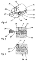
- the circuit removed from the molding tool shown in FIG. 4 and separated from the conductor foil 1 along the tear-out perforation 7 is combined to form a cylindrical housing body, as shown in FIG. 5.
- the pins 18 of the intermediate insulating layer 13 engage here in the holes 22 of the intermediate insulating layer 15 and hold the housing body 23 together to form a cylinder.
- the upper half-cylinder section 14 has a recess 24 into which the housing section 25 can still be pivoted.
- the housing section 25 encases the components of a special folding section which, although it is equipped with the components 2 in the plane of the conductor foil 1, is to be inserted into the housing body 23 as a housing section rotated by 90 ° to the other sections, so that e.g. a light-emitting diode 26 comes to lie outside in the field of vision.
- the electrical connection of the housing section 25 to the rest of the circuit takes place via the flexible conductor foil tongue 27, which is produced by a special contour of the tear-off perforation 7.
- FIG. 6 shows the housing section 25 in section before it has been inserted into the recess 24 of the housing section 14.
- 7 shows the closed housing body 23 with inserted housing section 25, the tongue 27 being folded in such a way that the light-emitting diode 26 comes to lie on the outside.
- FIG. 8 to 10 show an exemplary embodiment of an electrical display device with a device outer casing 28.
- the individual rectangular folding sections 4 with the components 2 are combined here by the plastic foam layers 29 and 30 applied from both sides to form flat, rectangular housing sections 31 to 34, as shown in FIG. 8. While the housing sections 31, 32 and 33 are in series one behind the other and have mutually parallel folding strips 5 with connecting conductors 3 between them, the housing section 34 with an LED display 35 has a folding strip 36 running at right angles to the other folding strips 5 remaining circuit connected.
- FIGS. 9 and 10 show the housing sections 31 to 33 folded like an accordion to form a sandwich construction, the display section 34 being folded onto the front of the sandwich package 31 to 33.
- the outer casing 28 provided for stiffening the housing body 23 and enclosing the sandwich package 31 to 34 is likewise formed here by a foam layer 37.
Landscapes
- Engineering & Computer Science (AREA)
- Microelectronics & Electronic Packaging (AREA)
- Manufacturing & Machinery (AREA)
- Casings For Electric Apparatus (AREA)
- Structure Of Printed Boards (AREA)
Claims (14)
- Procédure pour la fabrication des appareils électroniques durant une feuille conductrice (1) pourvu d'un circuit corrodé est placée, après être équipée des composantes éelectroniques (2) aux sections de pliage prédéterminées (4), pour adaption dans un outil de façonnage (10,11) reproduisant la forme géométrique de l'appareil et est envelopée d'un plastique durcisant pour former des éléments de boîte (12-15, 25, 31-34), avec le corps de boîte (23) formé du plastique durcissant étant subdivisé en éléments de boîte de telle sorte que les éléments de boîte (12-15,25) puissent, lors du pliage de la feuille conductrice, être emboîtes pour former un corps de boîte fermé, et ces éléments de boîte sont appliqués comme pièces façonnées en plastique individuel sur les sections de pliage de la feuille conductrice plate, encore non pliée, mais équipée, et ensuite le corps de boîte composé des sections de pliage individuelles est détaché le long d'une perforation pour arracher.
- Procédure leon la spécifiction 1, caractérisée par le fait que les moités de l'outil de façonnage sont approchées automatiquement d'une bande roulante équipée des composantes de circuit soudés, d'une part du côté d'insertion et d'autre part du côté de soudure, et qu'elles sont posées sur les sections de pliage, et ensuite du plastique est versé dans les cavités de la forme avec les moitiés de l'outil de façonnage suivant le mouvement vers l'avant de la bande lors du temps de durcissement du plastique et ensuite se réouvrant automatiquement pour se remettre en position initiale.
- Procédure selon le spécification 1 ou 2, caractérisée par le fait que les éléments de boîte reproduisant les contours du corps de boîte sont appliqués sur les sections de pliage du côté d'insertion de la feuille conductrice et des couches isolantes intermédiaires sont appliquées comme éléments de boîte dit côté de soudure et les couches isolantes intermédiaires des sections de pliage sont superposées lors du pliage.
- Procédure selon une ou plusieurs des spécifications 1 à 3, caractérisée par le fait qu'une mousse en plastique est utilisée comme plastique durcissant qui est versée seulement dans une des deux moitiés de l'outil de façonnage et que la feuille conductrice se trouvant dans la partie intérieure des sections de pliage es pourvu d'ouvertures pour la pénétration de la mousse en plastique.
- Procédure selon une ou plusieurs des spécifications 1 à 4, caractérisée par le fait que les éléments (12-15, 25, 31-34) du corps de boîte (23), lorsqu'ils sont emboîtés pour former une boîte fermée, sont joints l'un avex l'autre, comme un loqueteau, aux surfaces de contact à l'aide des chevilles saillantes préformées (18) et des creux situes face à elles
- Procédure selon une ou plusieures des spécfications 1 à 5, caractérisée par le fait qu'une bande de pliage (5) reste libre sur la feuille conductrice (1) entre les éléments de boîte en plastique adjacents (12,14 et 13,15 respectivement), la largeur de laquelle est adaptée à la hauteur des couches isolant es intermédiaires (13,15) après pliage.
- Procédure selon une ou plusieurs des spécifications 1 à 6, caractérisée par le fait que la feuille conductrice (1) est divisée en plusieurs sections de pliage rectangulaires (4) par des bandes de pliage (5) conseant parallélement et/ou perpendiculairement la feuille conductrice, et que sur ces sections de pliage rectangulaires, des éléments de boîte tabulaires en plastique (31-33) sont appliqués et pliés les uns sur les autres en construction "sandwich" pour former le corps de boite fermé (23).
- Procédure selon une ou plusieurs des spécifications 1 à 7, caractérisée par le fait que les éléments de boîte (12,14) du corps de boîte (23) appliqués du côté d'insertion (2) de la feuille conductrice (1) sont pourvus des creux moulés (24) dans lesquels on peut plier des sections de pliage avec petits éléments de boîte (25).
- Procédure selon une ou plusieurs des spécifications 1 à 8, caractérisée par le fait que les sections de pliage (4), qui doivent, avec leur élément de boîte appliqué en plastique (25), être insérées avec alternance dans le corps de boîte (23), sont liées par des traverses de raccordement (27), libres et sous forme de langues, de la feuille conductrice (1) au reste du circuit (2,3) sur la feuille conductrice (1).
- Procédure selon une ou plusieurs des spécifications 1 à 9, caractérisée par le fait que les éléments (31-34) joints les uns dans les autres pour former le corps de boîte fermé (23) sont enveloppés par un plastique durcissant constituant le revêtement de l'appareil.
- Procédure selon une ou plusieurs des spécifications 1 à 9, caractérisée par le fait que les éléments (12-15, 23, 31-34) joints les uns dans les autres pour former le corps de boîte fermé (23) sont glissés dans une boîte fermé préfabriquée et que la boîte est fermée par un couvercle situé à l'ouverture d'insertion.
- Procédure pour la fabrication d'un corps de boîte selon une ou plusieurs des spécefications 1 à 11, caractérisée par le fait que le plastique durcissant (21) est absorbé par des moitiés de l'outil de façonnage et sur le côté de soudure de la feuille conductrice (1), dans la partie des sections de pliage (4), au contour des éléments de boîte (12-15) et qui présentent des creux limités par des traverses (41,42), et que les sections de pliage (4) de la feuille conductrice (1) plate, pas encore pliée, mais équipée, sont fixées à la bande de pliage (5) ainsi qu'à la bande marginale formée par une perforation de détachement (7), étroitement entre les traverses intérieures et marginales (41,42) des moitiés de l'outil de façonnage (10,11).
- Procédure pour la fabrication d'un corps de boîte selon la spécification 12 caractérisée par le fait que les moitiés de l'outil de façonnage (10,11) pour toutes les sections de pliage (4) sont réunies pour former une moitié commune supérieure et inférieure de l'outil entier.
- Procédure pour la fabrication d'un corps de boîte selon les spécifications 12 et 13 caractérisée par le fait que les moitiés de l'outil de façonnage (10,11) qui présentent des chevilles de centrage (40) et percements de centrage sont pourvues congrument de trous de centrage (39) dans les bandes de pliage ou les bandes marginales (5,38) de la feuille conductrice équipée (1).
Applications Claiming Priority (2)
| Application Number | Priority Date | Filing Date | Title |
|---|---|---|---|
| DE19853512978 DE3512978A1 (de) | 1985-04-11 | 1985-04-11 | Verfahren und vorrichtung zur herstellung von elektronischen geraeten und nach dem verfahren hergestellte geraete |
| DE3512978 | 1985-04-11 |
Publications (3)
| Publication Number | Publication Date |
|---|---|
| EP0197516A2 EP0197516A2 (fr) | 1986-10-15 |
| EP0197516A3 EP0197516A3 (en) | 1988-08-17 |
| EP0197516B1 true EP0197516B1 (fr) | 1992-02-26 |
Family
ID=6267726
Family Applications (1)
| Application Number | Title | Priority Date | Filing Date |
|---|---|---|---|
| EP86104569A Expired - Lifetime EP0197516B1 (fr) | 1985-04-11 | 1986-04-03 | Méthode pour la production d'appareils électroniques |
Country Status (4)
| Country | Link |
|---|---|
| US (1) | US4730390A (fr) |
| EP (1) | EP0197516B1 (fr) |
| JP (1) | JPH0716101B2 (fr) |
| DE (1) | DE3512978A1 (fr) |
Families Citing this family (12)
| Publication number | Priority date | Publication date | Assignee | Title |
|---|---|---|---|---|
| US4939792A (en) * | 1987-11-16 | 1990-07-03 | Motorola, Inc. | Moldable/foldable radio housing |
| US4836651A (en) * | 1987-12-03 | 1989-06-06 | Anderson Richard A | Flexible circuit interconnection for a matrix addressed liquid crystal panel |
| US5093985A (en) * | 1989-06-30 | 1992-03-10 | John Houldsworth | Method of assembly for small electrical devices |
| DE3936906C2 (de) * | 1989-11-06 | 1995-02-02 | Telefunken Microelectron | Gehäuse für Kfz-Elektronik |
| AU6943191A (en) * | 1990-01-21 | 1991-07-25 | Sony Corporation | An electrical circuit apparatus using a flexible printed plate |
| FR2671935A1 (fr) * | 1991-01-22 | 1992-07-24 | Peugeot | Boitier de circuit electronique de puissance. |
| DE59609022D1 (de) * | 1995-06-15 | 2002-05-08 | Dyconex Patente Ag Zug | Verbindungssubstrat |
| DE19907295C1 (de) * | 1999-02-22 | 2001-02-08 | Univ Dresden Tech | Verfahren zur Montage elektronischer und/oder optischer Bauelemente und Baugruppen auf der Rückseite einseitig bestückter flexibler Leiterplatten |
| DE19960250A1 (de) * | 1999-12-14 | 2001-06-21 | Honsberg & Co Kg | Faltbare Leiterplatte |
| DE202004007207U1 (de) * | 2004-04-30 | 2004-12-09 | Würth Elektronik Rot am See GmbH & Co. KG | Schaltungsträger |
| JP4718434B2 (ja) * | 2006-08-16 | 2011-07-06 | 富士通株式会社 | 電子機器 |
| JP4589431B2 (ja) * | 2008-11-10 | 2010-12-01 | パナソニック株式会社 | 基板取付け方法及び基板収納体 |
Family Cites Families (4)
| Publication number | Priority date | Publication date | Assignee | Title |
|---|---|---|---|---|
| DE2423144A1 (de) * | 1974-05-13 | 1975-11-20 | Siemens Ag | Flexibler schaltungstraeger |
| US4085433A (en) * | 1976-11-22 | 1978-04-18 | Baranowski Conrad J | Method and apparatus for improving packaging density of discrete electronic components |
| WO1982004161A1 (fr) * | 1981-05-21 | 1982-11-25 | Ishihara Shokichi | Dispositif permettant d'empecher la copie d'un programme d'ordinateur |
| US4667401A (en) * | 1985-11-26 | 1987-05-26 | Clements James R | Method of making an electronic device using an uniaxial conductive adhesive |
-
1985
- 1985-04-11 DE DE19853512978 patent/DE3512978A1/de active Granted
-
1986
- 1986-04-03 EP EP86104569A patent/EP0197516B1/fr not_active Expired - Lifetime
- 1986-04-10 JP JP61081255A patent/JPH0716101B2/ja not_active Expired - Lifetime
- 1986-04-11 US US06/851,322 patent/US4730390A/en not_active Expired - Lifetime
Also Published As
| Publication number | Publication date |
|---|---|
| JPH0716101B2 (ja) | 1995-02-22 |
| EP0197516A2 (fr) | 1986-10-15 |
| DE3512978A1 (de) | 1986-10-16 |
| EP0197516A3 (en) | 1988-08-17 |
| US4730390A (en) | 1988-03-15 |
| JPS61281593A (ja) | 1986-12-11 |
| DE3512978C2 (fr) | 1990-02-22 |
Similar Documents
| Publication | Publication Date | Title |
|---|---|---|
| EP0197516B1 (fr) | Méthode pour la production d'appareils électroniques | |
| EP0756244B1 (fr) | Unité électronique et procédé de fabrication de cette unité | |
| AT410728B (de) | Verfahren zum einbetten zumindest einer flexiblen leiterbahnfolie in kunststoff, leiterbahneneinheitsowie einbettungseinheit hiefür | |
| EP1199913B1 (fr) | Méthode de fabrication d'unités comprenant une feuille de circuit et un boítier de support | |
| DE953992T1 (de) | Oberflächenmontierte leitfähige Polymer-Bauelemente und Verfahren zur Herstellung derselben | |
| DE1586136B1 (de) | Verfahren zur kontinuierlichen vorbereitung einer vielzahl von elektronischen schaltelementen fuer die pruefung und montage auf gedruckte schaltungen | |
| DE19741047C2 (de) | Elektronisches Zündschloss für Kraftfahrzeuge | |
| DE69127799T2 (de) | Kunststoffgekapseltes Halbleiterbauteil und Verfahren zu dessen Herstellung | |
| DE2342238A1 (de) | Verfahren zur erzeugung elektrisch isolierter durchgangsverbindungen in einer leitenden platte fuer eine elektrische vielplatten-schaltungsanordnung | |
| DE2941613A1 (de) | Traegerplaettchen mit leiterbahnen und ggf. elektronischen schaltungsbauteilen sowie verfahren zu seiner herstellung | |
| EP0863530A2 (fr) | Panneau à circuit électrique et procédé de fabrication | |
| DE4436523B4 (de) | Verfahren zur Herstellung eines elektronischen Gerätes und Drehzahlsensor mit einer elektronischen Schaltung | |
| DE3880067T2 (de) | Leiterplatten für hohe Ströme und Verfahren zur Herstellung. | |
| DE69216377T2 (de) | Form und Verfahren zur Herstellung von Kunststoffpackungen für integrierte Schaltungen die eine freie metallische Wärmesenke enthalten zur Inspektion der Lötverbindung | |
| DE3318717C1 (de) | Verfahren zum Herstellen von Leiterplatten mit starren und flexiblen Bereichen | |
| DE19818452B4 (de) | Elektronische Schaltung mit einer in Gießharz eingebetteten Leiterplatte und Verfahren zu ihrer Herstellung | |
| DE19719436C2 (de) | Spritzgußgehäuse | |
| DE2423144A1 (de) | Flexibler schaltungstraeger | |
| EP0891602B1 (fr) | Carte electronique avec un boitier pour un circuit electronique implantable dans lequelle boitier , et procede de fabrication d'une telle carte | |
| DE20316051U1 (de) | EMV-Modul | |
| DE19528731C2 (de) | Verfahren zum Schützen von Bauteilen | |
| WO2013178212A2 (fr) | Support pour composant de véhicule à moteur et procédé de fabrication dudit support | |
| DE102006028816B4 (de) | Verfahren zum getakteten, kontinuierlichen Herstellen von beidseitig umspritzten flexiblen Leiterplatten | |
| DE4237496C2 (de) | Steckverbindung | |
| DE3603912A1 (de) | Elektronischer netzwerk-baustein und verfahren zur herstellung desselben |
Legal Events
| Date | Code | Title | Description |
|---|---|---|---|
| PUAI | Public reference made under article 153(3) epc to a published international application that has entered the european phase |
Free format text: ORIGINAL CODE: 0009012 |
|
| AK | Designated contracting states |
Kind code of ref document: A2 Designated state(s): CH FR IT LI NL SE |
|
| PUAL | Search report despatched |
Free format text: ORIGINAL CODE: 0009013 |
|
| AK | Designated contracting states |
Kind code of ref document: A3 Designated state(s): CH FR IT LI NL SE |
|
| 17P | Request for examination filed |
Effective date: 19890216 |
|
| 17Q | First examination report despatched |
Effective date: 19900531 |
|
| GRAA | (expected) grant |
Free format text: ORIGINAL CODE: 0009210 |
|
| AK | Designated contracting states |
Kind code of ref document: B1 Designated state(s): CH FR IT LI NL SE |
|
| ITF | It: translation for a ep patent filed | ||
| ET | Fr: translation filed | ||
| PLBE | No opposition filed within time limit |
Free format text: ORIGINAL CODE: 0009261 |
|
| STAA | Information on the status of an ep patent application or granted ep patent |
Free format text: STATUS: NO OPPOSITION FILED WITHIN TIME LIMIT |
|
| 26N | No opposition filed | ||
| EAL | Se: european patent in force in sweden |
Ref document number: 86104569.8 |
|
| PGFP | Annual fee paid to national office [announced via postgrant information from national office to epo] |
Ref country code: SE Payment date: 19960411 Year of fee payment: 11 |
|
| PGFP | Annual fee paid to national office [announced via postgrant information from national office to epo] |
Ref country code: CH Payment date: 19960422 Year of fee payment: 11 |
|
| PGFP | Annual fee paid to national office [announced via postgrant information from national office to epo] |
Ref country code: NL Payment date: 19960430 Year of fee payment: 11 |
|
| PG25 | Lapsed in a contracting state [announced via postgrant information from national office to epo] |
Ref country code: SE Effective date: 19970404 |
|
| PG25 | Lapsed in a contracting state [announced via postgrant information from national office to epo] |
Ref country code: LI Free format text: LAPSE BECAUSE OF NON-PAYMENT OF DUE FEES Effective date: 19970430 Ref country code: CH Free format text: LAPSE BECAUSE OF NON-PAYMENT OF DUE FEES Effective date: 19970430 |
|
| PG25 | Lapsed in a contracting state [announced via postgrant information from national office to epo] |
Ref country code: NL Effective date: 19971101 |
|
| REG | Reference to a national code |
Ref country code: CH Ref legal event code: PL |
|
| NLV4 | Nl: lapsed or anulled due to non-payment of the annual fee |
Effective date: 19971101 |
|
| EUG | Se: european patent has lapsed |
Ref document number: 86104569.8 |
|
| PGFP | Annual fee paid to national office [announced via postgrant information from national office to epo] |
Ref country code: FR Payment date: 20030428 Year of fee payment: 18 |
|
| PG25 | Lapsed in a contracting state [announced via postgrant information from national office to epo] |
Ref country code: FR Free format text: LAPSE BECAUSE OF NON-PAYMENT OF DUE FEES Effective date: 20041231 |
|
| REG | Reference to a national code |
Ref country code: FR Ref legal event code: ST |
|
| PG25 | Lapsed in a contracting state [announced via postgrant information from national office to epo] |
Ref country code: IT Free format text: LAPSE BECAUSE OF NON-PAYMENT OF DUE FEES;WARNING: LAPSES OF ITALIAN PATENTS WITH EFFECTIVE DATE BEFORE 2007 MAY HAVE OCCURRED AT ANY TIME BEFORE 2007. THE CORRECT EFFECTIVE DATE MAY BE DIFFERENT FROM THE ONE RECORDED. Effective date: 20050403 |