EP0196631A2 - Integrable high frequency, wide band and superlinear amplifier and its fabrication - Google Patents
Integrable high frequency, wide band and superlinear amplifier and its fabrication Download PDFInfo
- Publication number
- EP0196631A2 EP0196631A2 EP86104252A EP86104252A EP0196631A2 EP 0196631 A2 EP0196631 A2 EP 0196631A2 EP 86104252 A EP86104252 A EP 86104252A EP 86104252 A EP86104252 A EP 86104252A EP 0196631 A2 EP0196631 A2 EP 0196631A2
- Authority
- EP
- European Patent Office
- Prior art keywords
- amplifier
- high frequency
- fabrication
- stage
- integrated
- Prior art date
- Legal status (The legal status is an assumption and is not a legal conclusion. Google has not performed a legal analysis and makes no representation as to the accuracy of the status listed.)
- Withdrawn
Links
- 238000004519 manufacturing process Methods 0.000 title claims abstract description 21
- 238000000034 method Methods 0.000 claims abstract description 61
- 238000000926 separation method Methods 0.000 claims abstract description 11
- 238000005516 engineering process Methods 0.000 claims abstract description 10
- 238000005476 soldering Methods 0.000 claims description 4
- 238000012937 correction Methods 0.000 claims description 3
- 230000007547 defect Effects 0.000 claims 1
- 230000017525 heat dissipation Effects 0.000 claims 1
- 239000004065 semiconductor Substances 0.000 claims 1
- 238000003466 welding Methods 0.000 claims 1
- 238000013461 design Methods 0.000 abstract description 27
- 230000010354 integration Effects 0.000 abstract description 19
- 230000008901 benefit Effects 0.000 abstract description 7
- 230000003321 amplification Effects 0.000 abstract description 2
- 238000006243 chemical reaction Methods 0.000 abstract description 2
- 238000003199 nucleic acid amplification method Methods 0.000 abstract description 2
- 239000000835 fiber Substances 0.000 abstract 1
- 230000009466 transformation Effects 0.000 abstract 1
- 230000010363 phase shift Effects 0.000 description 10
- XUIMIQQOPSSXEZ-UHFFFAOYSA-N Silicon Chemical compound [Si] XUIMIQQOPSSXEZ-UHFFFAOYSA-N 0.000 description 9
- 239000003990 capacitor Substances 0.000 description 9
- 229910052710 silicon Inorganic materials 0.000 description 7
- 239000010703 silicon Substances 0.000 description 7
- 238000010586 diagram Methods 0.000 description 6
- 230000002708 enhancing effect Effects 0.000 description 6
- 239000011094 fiberboard Substances 0.000 description 4
- 238000002955 isolation Methods 0.000 description 3
- 238000013459 approach Methods 0.000 description 2
- 239000000919 ceramic Substances 0.000 description 2
- 230000008859 change Effects 0.000 description 2
- 238000004891 communication Methods 0.000 description 2
- 239000010408 film Substances 0.000 description 2
- 239000013307 optical fiber Substances 0.000 description 2
- 230000008569 process Effects 0.000 description 2
- 239000010409 thin film Substances 0.000 description 2
- RYGMFSIKBFXOCR-UHFFFAOYSA-N Copper Chemical compound [Cu] RYGMFSIKBFXOCR-UHFFFAOYSA-N 0.000 description 1
- BQCADISMDOOEFD-UHFFFAOYSA-N Silver Chemical compound [Ag] BQCADISMDOOEFD-UHFFFAOYSA-N 0.000 description 1
- 238000004458 analytical method Methods 0.000 description 1
- 238000010923 batch production Methods 0.000 description 1
- 239000000969 carrier Substances 0.000 description 1
- 239000011248 coating agent Substances 0.000 description 1
- 238000000576 coating method Methods 0.000 description 1
- 239000011889 copper foil Substances 0.000 description 1
- 239000013078 crystal Substances 0.000 description 1
- 230000002950 deficient Effects 0.000 description 1
- 238000009826 distribution Methods 0.000 description 1
- 230000000694 effects Effects 0.000 description 1
- 230000006872 improvement Effects 0.000 description 1
- 230000006698 induction Effects 0.000 description 1
- 239000000123 paper Substances 0.000 description 1
- 238000012545 processing Methods 0.000 description 1
- 230000004044 response Effects 0.000 description 1
- 229910052709 silver Inorganic materials 0.000 description 1
- 239000004332 silver Substances 0.000 description 1
- 239000000758 substrate Substances 0.000 description 1
Images
Classifications
-
- H—ELECTRICITY
- H03—ELECTRONIC CIRCUITRY
- H03F—AMPLIFIERS
- H03F3/00—Amplifiers with only discharge tubes or only semiconductor devices as amplifying elements
- H03F3/189—High-frequency amplifiers, e.g. radio frequency amplifiers
- H03F3/19—High-frequency amplifiers, e.g. radio frequency amplifiers with semiconductor devices only
- H03F3/195—High-frequency amplifiers, e.g. radio frequency amplifiers with semiconductor devices only in integrated circuits
-
- H—ELECTRICITY
- H03—ELECTRONIC CIRCUITRY
- H03F—AMPLIFIERS
- H03F1/00—Details of amplifiers with only discharge tubes, only semiconductor devices or only unspecified devices as amplifying elements
- H03F1/42—Modifications of amplifiers to extend the bandwidth
- H03F1/48—Modifications of amplifiers to extend the bandwidth of aperiodic amplifiers
-
- Y—GENERAL TAGGING OF NEW TECHNOLOGICAL DEVELOPMENTS; GENERAL TAGGING OF CROSS-SECTIONAL TECHNOLOGIES SPANNING OVER SEVERAL SECTIONS OF THE IPC; TECHNICAL SUBJECTS COVERED BY FORMER USPC CROSS-REFERENCE ART COLLECTIONS [XRACs] AND DIGESTS
- Y10—TECHNICAL SUBJECTS COVERED BY FORMER USPC
- Y10T—TECHNICAL SUBJECTS COVERED BY FORMER US CLASSIFICATION
- Y10T29/00—Metal working
- Y10T29/49—Method of mechanical manufacture
- Y10T29/49002—Electrical device making
- Y10T29/49117—Conductor or circuit manufacturing
- Y10T29/49124—On flat or curved insulated base, e.g., printed circuit, etc.
- Y10T29/4913—Assembling to base an electrical component, e.g., capacitor, etc.
- Y10T29/49133—Assembling to base an electrical component, e.g., capacitor, etc. with component orienting
- Y10T29/49137—Different components
Definitions
- This invention relates to an integrable high frequency, wide bandwidth and superlinear amplifier and its fabrication method. It deals with high frequency, wide bandwidth, high stability, low noise, high reliability, deep negative feedback and improvement of the technology of integration.
- the amplifier also may be applied to a weak feedback or a D.C. and audio circuits.
- the impedance of such amplifier could be adjusted to desirable values.
- a series of universal integrated fundamental amplifier could be designed and fabricated.
- the objects of this invention are to simplify the design of circuits and propose a new fabrication method for integration to produce universal and serialised integrated circuits with many advantages, such as high frequency, wide bandwidth, superlinearity, high stability, low noise, high reliability and deep feedback (or weak feedback), which will be widely used in many areas. Therefore, it has overcome many disadvantages in the existing techniques, such as difficulties for adjustments and integration, etc.
- advantages such as low modulation distortion, low transit distortion, negative feedback about 180° and utilization of transistors with low characteristic frequency.
- the circuit dsign could be simplified and the number of correcting elements could greatly be reduced (for example, 1-7 elements needed).
- a new integration method for fabricating the invented amplifier is proposed. If these two new ideas are applied, the amplifier produced could work at about 10 GHZ or down to D.C. frequency.
- the new integration technology used in this invention mainly adopts separation method, in which the total of the feedback circuit length is approximately equal to the size of the silicon chip or smaller than that size in order to reduce the parasitical capacitance, inductance of ground wires and spacial induction to the least extent.
- the design of circuits, mentioned in this invention utilizes basically two-narrow-one-wide of two-wide-one-narrow method combined with Bode method.
- the design of this invention presents a new method with least number of correcting elements.
- the new integration method for fabrication and the method controlling parasitical parameters of discrete elements have guaranteed the implementation of above circuits.
- the Bode method, two-wide-one-narrow, two-narrow-one-wide method may respectively combine with the above mentioned integration techniques or the control method for discrete elements. Because deeper negative feedback is applied, specifications, such as harmonies distortion and stability of the invented amplifier may improve to a factor of (1+K ⁇ ), depending on feedback intensity.
- the invented amplifier is a basic amplifier, and it could be cascaded for consecutive multistage multiplication.
- adjustable impedance may improve reflecting and standing waves' characteristics.
- switch control circuits are inserted to feedback loop or input and output terminals, analog signals may be converted into PAM signals. Because the amplifier can operate at high frequency, it can be served as a fast processing for other digital circuits.
- the amplifiers of this invention When it is applied to communication systems, because the amplifiers of this invention have excellent linearity and impedance adjustability with no transformers, more than 90 % of transformers may be eliminated in voice terminals and line terminals bays.
- Devices for modulators are available from markets now, and carriers distribution and concentration all employ active distributors. Any characteristics required, such as, constant current output (high impedance), low resistance concentration, which improve concentration accuracy and reflection performances, can be obtained.
- single crystal chip filter may be used.
- the amplifier is needed to work at about 10 MHz. However, simple and high frequency performance of this invented amplifier may easily meet the requiremens.
- FET of Vg s of 1200 V are used in balance inputs, and high-voltage transistors or high-power and high-voltage FET are employed in balanced outputs. Integrated circuits are divided into blocks according to bays.
Landscapes
- Engineering & Computer Science (AREA)
- Power Engineering (AREA)
- Microelectronics & Electronic Packaging (AREA)
- Amplifiers (AREA)
Abstract
An integrable, high frequency superlinear amplifier and its fabrication method. Which belongs to the basic amplifier fabrication field related to the negative feedback and signal conversion.The adoption of such methods as compromising and the separation of integration may solve the problems in technology like the complication in Kp design, the large quantity of elements, and the difficulties in integration, generalization, the serialised and universal design and fabrication.The amplifiers have following advantages: high frequency, wide band, superlinera, high stability, integration, high reliability, low noise, antigravitation, serialised and universal fabrication, and adjustable impedance without a transformer.It may be used digital pulse amplification and transformation near 10GHZ, in meters, automation, video and audio frequencies, telecommunication systems, fiber optic systems, active analogue computation, and in other cases which call for high requirements such as military and aerospace uses.
Description
- This invention relates to an integrable high frequency, wide bandwidth and superlinear amplifier and its fabrication method. It deals with high frequency, wide bandwidth, high stability, low noise, high reliability, deep negative feedback and improvement of the technology of integration. The amplifier also may be applied to a weak feedback or a D.C. and audio circuits.
- If the above characteristic is fulfilled and transformer is not used, the impedance of such amplifier could be adjusted to desirable values. With this invention, a series of universal integrated fundamental amplifier could be designed and fabricated.
- In order to make an amplifier with better performance, such as high frequency, wide bandwidth and superlinearity or stability in the parameters, deep feedback is generally used. However, two serious problems would occur: first, the design for a high frequency and deep feedback amplifier becomes more complicated; for example, a line amplifier with bandwidth of 0.3 MHZ--9MHZ has more than 50 K correcting elements, in which standard Bode method is used. Because there are many elements, it is not possible to make those parameters of the elements completely consistent, and also it is difficult to control parasitical parameters. Besides, precise elements are required. Due to the above mentioned facts, it is hard to integrate an amplifier with high performance into integrated circuit. Secondly, reverse bias isolation is generally used in integrated circuits. However, both isolation capacitance and parasitical inductance are large. Thus, the parasitical parameters are not easily and effectively controlled, and any additional phase shift must be considered for a high frequency circuit.
- Those amplifiers are usually fabricated by discrete elements or hybrid integration with thick and thin film technics. Therefore, each amplifier must be carefully designed and adjusted, and the rate of products to meet the specification are less than 10 410 in one batch process. It is very difficult to fabricate in mass and integration production. Also, it is impossible to produce a series and universal integrated amplifier with high quality, or to provide a simple design for such amplifier with high productivity, which could be constructed by discrete elements.
- It is expected that a high frequency (or low frequency) wide band superlinear amplifier with simple design, less correcting elements, better stability independent of transistors' characteristics, small additional phase shift, less cost and integrated circuits will be widely applied to amplification for analog signals and PAM, PCM signals, precise and high speed automation system, communication system, military and aerospace equipments and audio music systems.
- Up to date for application, no high frequency wide band superlinear, universal series integrated products and its fabrication method explained in this invention has been found. For example, US-PS 3 774 118, 3 530 392, 2 959 741, 2 885 494 etc. have not proposed any simplified design method for KP design and new methods for integration. Particularly, no idea for an universal and serialised design and production with discrete and integrated elements has been provided.
- The objects of this invention are to simplify the design of circuits and propose a new fabrication method for integration to produce universal and serialised integrated circuits with many advantages, such as high frequency, wide bandwidth, superlinearity, high stability, low noise, high reliability and deep feedback (or weak feedback), which will be widely used in many areas. Therefore, it has overcome many disadvantages in the existing techniques, such as difficulties for adjustments and integration, etc. There are two types for the circuit design: two-stage amplifier and three-stage amplifier. If this invention is applied to an audio system, it would posses many advantages: such as low modulation distortion, low transit distortion, negative feedback about 180° and utilization of transistors with low characteristic frequency. There are two main new ideas in this invention. First, the circuit dsign could be simplified and the number of correcting elements could greatly be reduced (for example, 1-7 elements needed). Secondly, a new integration method for fabricating the invented amplifier is proposed. If these two new ideas are applied, the amplifier produced could work at about 10 GHZ or down to D.C. frequency. The new integration technology used in this invention mainly adopts separation method, in which the total of the feedback circuit length is approximately equal to the size of the silicon chip or smaller than that size in order to reduce the parasitical capacitance, inductance of ground wires and spacial induction to the least extent. The design of circuits, mentioned in this invention utilizes basically two-narrow-one-wide of two-wide-one-narrow method combined with Bode method. The design of this invention presents a new method with least number of correcting elements. The new integration method for fabrication and the method controlling parasitical parameters of discrete elements have guaranteed the implementation of above circuits. In this invention the Bode method, two-wide-one-narrow, two-narrow-one-wide method may respectively combine with the above mentioned integration techniques or the control method for discrete elements. Because deeper negative feedback is applied, specifications, such as harmonies distortion and stability of the invented amplifier may improve to a factor of (1+Kβ), depending on feedback intensity. The invented amplifier is a basic amplifier, and it could be cascaded for consecutive multistage multiplication.
-
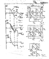
- 1. Three-stage type with discrete elements: Compromise between two-narrow-one-wide method and Bode method is used. (In order to improve the performance two-narrow-one-wide method, two-wide-one-narrow and Bode methods may respectively combine with the following integrated circuit techniques or control method for descrete elements). The key points of compromise design are the following: first, the bandwidth of the amplifier with widewidth must meet following requirements: If the gain curve for two narrow bandwidth stages passes corresponding frequency through 0 point to 6dB as shown in Fig. 1 [1], the peak point, as shown in Fig. 1 [2], of the enhancing curve with single capacitor for wide bandwidth stage should be ahead of above frequency [1]. Therefore the resulting curve of three stages (see Fig. 2 [3]) below the 0 point is approximately flat (Fig. 2 [4]). Then, the shadow section shown in Fig. 2 [7] by dash lines should be removed at the -40dB/10 f descending slope, which is shown in Fig. 2 between [5] and [6j. A R3L3C3 network is used to absorb the dash area section. The above single capacitor enhancement method is implemented with R1C1R2C2 shown in Fig. 4 or with RC in Fig.5. Through these two steps, the resulting three-stage curve approaches the least Bode phase shift curve (Fig. 3 [8]. In order to reach more precise correction or deeper feedback, more correcting elements can be incorporated into Fig. 4 and Fig. 5 according to Bode method. That can make the resulting curve further approach ideal curve. For example, the frequency [5] in Fig. 2 is enhanced to be a prominent point (with RLC serial enhancement network), and other frequencies in Fig. 2Z over and above [6] can be enhanced with a single capacitor correcting or RLC enhancement network. However, if the bandwidth of wideband stage is sufficiently large and the parasitical parameters are well controlled, the further precise correction above is not required, and only R1C1 or R2C2 are needed. Then, it should be considered whether it is necessary to remove dash area section in Fig. 2 [7] by R3L3C3. If R3L3C3 are not used, this circuit becomes the same one as designated by the name of two-narrow-one-wide or two-wide-one-narrow method. The wide bandwidth stage can be designed at any stage. If R2C2 are used to increase the bandwidth, the increasing coefficient of bandwidth is (1+ Kβ). In order to reach the above purpose, calculated and experimental curves are usually plotted in a double logarithum plotting paper in design, and frequency [2] for wide-bandwidth stage and the dB increment at [2] are then determined. The increment at frequency [2] is usually 3-26 dB. The more the increment, the less the phases shift at [1]. The amplitude of increment is determined by RIC1 or R2C2 in Fig. 4. Zfl, Zf2 play a role of current and voltage feedback, and adjust the impedance to the desired value. The feedback type with three stages only absorbs a little input and output signals. It is good for low noise and low distortion. The highest frequency of around transistor 0.9 fT can be employed in this design.
- 2. Modified three-stages type:
If the output is connected to collector for second stage (Fig. 5), the wide bandwidth stage for enhancing and widening frequency range should be at third stage. This stage is specialized in negative feedback conversion, and its feedback intensity is determined by Re3 and RL3 or the different tapped points at RL2. But Re3 mainly specifies bandwidth of BG3, and the peak point of enhancement [2] is determined by RC in Fig. 5. The feature of this method is to make the bandwidth of wide bandwidth stage reach to maximum value. This is due to the fact that third stage is a feedback attenuation stage, and larger Re3 can be used. According to the feedback of this stage, bandwidth increases to a factor of (1+ Kβ), for example, frequency [2] can reach to (0.5-1.0) fT. If increases, frequency [2] can increase too. The advantage for modified three-stage type is that the operating frequency is higher than three-stage type, for example, it can reach to about (0.9-1.0)fT. Gain, feedback, noise figure and harmonic distortion all are better than the following two-stage type. - 3. Two-stage type:
- Shortcomings for usual two-stage type are that its impedances can not be adjusted, open-loop gain is low and noise figure and harmonic distortion are poor. In this invention NPN and PNP transistors are mixed together and both current and voltage feedback are used (Fig. 6). Feedback points for Zfl, Zf2 can be moved upon Re2 RL2 taps to adjust required output and input impedances. If some suitable cases, Zf2 can be cancelled and shorted out, and Rel and RL2 are merged into one resistance. This resistance specifies current- series feedback. Thus, it improves the open-loop gain, noise figure and harmonic distortion. Its drawbacks are that specifications, such as gains, etc. are not as good as three-stage type and modified three-stage type. Because influences of Rel Re2 existing in open loop are larger than above three-stage and modified three-stage type, gain is lower than those two circuits.
- All these above three design methods introduce noise less than 0.5-6 dB and can adjust impedances. Even without transformers, all above mentioned excellent performances can be obtained. It is very important for integration and miniaturisation.
- If the peak point is enhanced by 3-26 dB with RC at the frequency [5] in Fig. 2, phase shift can be controlled within approximate minus 180° in the bandwidth used, and additional phase shift is in the range of 0° - 5°. Because various instantaneous music waveforms include high-order harmonics, and the loudspeaker's reserve electromotive forces and burst stopping voltage also have high frequency components, this amplifier can ensure approximate 180° negative feedback with 0°-5° additional phase shift for these high frequency components. Thus, it improves a variety of instantaneous characteristics. Meanwhile, transistors employed require lower fT than that by conventional design. It, then, results in low cost. This method can be applied to two-stage, three-stage and multistage circuits.
- 4. Fabrication for integrated circuits:
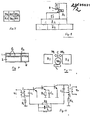
- According to the above analyses, the following configurations for integrated circuits have been devised (Fig. 8). It ensures all the connecting wire length for electrodes within 0.01-0.5 mm. The wire length from emitter must be as short as possible to avoid . additional phase shift. The sharp edges of ground wire El reduces inductance from the ground wire on the silicon ship. If there is no direct ground, the sharp edges contacts can be omitted. Meanwhile, the height for E1 is reduced, and it is good for further reducing the connecting wire. A2 is a ceramic heat sink, and Al is a ceramic substrate for fabricating ground wire El and film R, L, C. In order to close to other silicon chips R, L, C should be at the top upper part of A1. A1, El, RLC are glued together, based on A1 and prefabricated separately, and all of them are adhered to A2. B is the soldering pont for R,L,C with silver coating. The thickness of El and its distance from silicon chip have influences on the length of all connecting wire and parasitical capacitance between the ground and the silicon chips. Meanwhile, in order to reduce the inductance of ground wire, E1 should be made thinner and wider, for example, E1 with thickness of 0.01-0.2 mm and width of 1-6 mm. Thus, the ground wire inductance is less than conventional integrated circuits and parasitical capacitors also are very small. The silicon chip is square or rectangular in shape. After being fabricated on the whole circular chip successfully, a small portion is cut off from chip, which contans three transistors. RLC may be integrated and fabricated first, and they are then soldered on A2. Later, transistors and RLC are separated from requirements. Therefore, individual parasitical parameters are obtained with least distance and fabrication exploits integration techniques. Because the size of silicon chip depends on transistors, the total length of loop may be controlled by less than 0.1-10 mm, which is less than or approximately equal to the size of silicon chip. If inductionless capacitors are used, the virtual total length is much more shorter. In case of special requirements or generalization needed, manufacturer may leave rooms for RLC, where customers may put various film-elements on the top of integrated circuits themselves or they may ask manufacturer to fabricate in customer design way. Manufacturers may develop a variety of RLC chip elements and publish products' manual to spreed applications. The above integrated circuits with each parasitical capacitor of less then 0.01-50 pF can be fabricated together first and then separated (Fig. 7). It is allowed to punch holes on E2 to reduce parasitical capaciters.
- By the above mentioned design, each transistor has optimal independent parasitical parameters, and it fabrication employs integrated techniques. Thus, it is good for mass production. Drawbacks, such as reverse-bias isolation capacitor and other large parasitical parameters, by conventional integrated circuits are eliminated. Because modern soldering is precise and very fast, the design of this invention ensures precise geometrical sizes. In order to improve reliability, the defective sections in chips may be removed by a computer-controlled location detecting method.
- 5. Amplifier with discrete elements and its fabrication:
- If integrated techniques are not available, it is very simple and easy to employ the design of this invention. And also its performances are better than existing known techniques. First, three-layer printed circuit boards are used (Fig. 9) (two-layer printed circuit boards may also be used). The upper and lower layers are of copper foil, G1 is a metallized hole, which prevents soldered elements from pulling out. Third layer mainly serves as a ground wire. If grounding is needed, it must be connected to the large area ground wire on third layer. However, the first fiber board should be thin, and all interconnections should be on the first layer. A few wires may be laid on second layer, but the circular soldering joints should be small and the second fiber board is thick in order to make parasitical capacitance small enough and ground inductance small enough too. If the requirement for tensile strength is not serious, two-layer board can be used. Now the arrangements for elements are considered (Fig. 10). Transistors, emitter capacitance and feedback capacitors which have influences on A.C. loop length, are laid between two transformers, where the interval between transformers is about 3-20 mm, and all other resistances are laid outside the transformer. Thus total loop length is controlled within 10-65 mm. Ground wires here are considered to be an inductionless ground wire, and it can eliminate additional phase shift, which is very important. Multiple- wire of 0.05-0.3 mm each are parallelly wound and interleaved, and all layers are interlaced with each other to obtain small parasitical capacitance and leak inductance in transformers.
- Advantages of the invention over known techniques:
- KP design is greatly simplified; correcting elements greatly reduced; and no precise elements are required; design and fabrication become convenient; fabrication can exploit integrated techniques; parasitical parameters can be well controlled; process technology becomes simple; Because of simplified design, small number of elements and integration, it is convenient to produce serialised, universal and low-cost integrated products or discrete products used in various fields; products may obtain many excellent characteristics, such as high frequency, wide bandwidth, superlinearity, high stability, high reliability, low noise, antigravitation integration and adjustable impedance under no transformers.
- If frequency used is lower, the circuit design of this invention combined with conventional integrated circuit process techniques may be used or conventional design combined with separation method of this invention and integrated techniques may be employed.
- Because of the above mentioned advantages the amplifier may be applied to various systems as follows:
- If it is used to amplify impulse digital signals, various characteristics, such as low noise, adjustable impedance and high frequency, etc., are obtained, especially, adjustable impedance may improve reflecting and standing waves' characteristics. If switch control circuits are inserted to feedback loop or input and output terminals, analog signals may be converted into PAM signals. Because the amplifier can operate at high frequency, it can be served as a fast processing for other digital circuits.
- If it is used in products with high requirements, such as instruments, automation control, military and aerospace technology, various advantages of the amplifier, such as integration, miniaturization, antigravitation, high frequency, widebandwidth, superlinearity, high stability, low noise and adjustable impedance without transformers are exploited.
- When the amplifier is applied to analog operation and active filters, characteristics as low noise and high frequency are employed.
- When it is applied to emitting and receiving equipments for broadcast and television, superlinearity is used to solve distortion problem. In addition, no matter how AGC voltages change the passband characteristics remain invariant in AGC adjustment for fixed impedance. Thus, it can improve performances of present various emitters, receivers, televisions and radio receiver circuits. This is because amplifier directly change gain through controlling the magnitude of feedback impedance. Meanwhile, introduced noise figure is less than 3 dB.
- When it is applied to an audio system, such as receivers, amplifiers, tape recorder, for domestic and professional equipments, low cost and the following better characte-- ristics are obtained. This is because of lower fT and moderatenlinear transistors are used in this invention to obtain low harmonic distortion, intermodulation distortion and fast instantaneous distortions. If it is operated in the range of 0.1--0.6 prominent peak frequency, only 0--100 additional phase shifts are introduced by raising peak C51 outside passband to 3--26 dB. It ensures approximate 180° negative feedback for audio-high frequencies, and demonstrates very fast response speed. Even for burst stopping music waveforms and loudspeaker's reverse electromotive forces, which have rich high frequency components, they can be sufficiently fast suppressed. Therefore, not only circuit problems but also the match problems between loudspeakers and amplifiers interfaces as well have been solved. There is lower requirements for transistors.
- When it is applied to communication systems, because the amplifiers of this invention have excellent linearity and impedance adjustability with no transformers, more than 90 % of transformers may be eliminated in voice terminals and line terminals bays. Devices for modulators are available from markets now, and carriers distribution and concentration all employ active distributors. Any characteristics required, such as, constant current output (high impedance), low resistance concentration, which improve concentration accuracy and reflection performances, can be obtained. In order to reduce volume, single crystal chip filter may be used. Thus, the amplifier is needed to work at about 10 MHz. However, simple and high frequency performance of this invented amplifier may easily meet the requiremens. FET of Vgs of 1200 V are used in balance inputs, and high-voltage transistors or high-power and high-voltage FET are employed in balanced outputs. Integrated circuits are divided into blocks according to bays.
- When the amplifier is applied to optical fiber systems, characteristics, as simplicity, integration, low noise and low cost, are more attractive. Especially, in optical fiber analog systems, various above good performances, as simplicity, effectiveness, superlinearity and high frequency, are shown.
-
- Fig. 1 - Fig. 3 are schematic diagrams of curves for two-narrow-one-wide and Bode methods. In Fig. 1 curve with -40 dB/10 f demonstrates one for two-narrow stage, and curve with -20 dB/10 f expresses characteristic for wideband stage. Frequency [2] is the enhancing peak. When it is used in audio circuits, frequency [5] corresponds enhancing peak for narrow band stage.
- Fig. 4 is three-stage configuration.
- Fig. 5 is modified three-stage configuration.
- Fig. 6 is two-stage configuration. R1,C1; R2C2 are enhancing elements for peak in Fig. 4, and RLC are absorbing network for shadow section (7), Zfl, Zf2 are feedback impedances.
- Fig. 7 is a schematical diagram for integrated separation method.
- Fig. 8 is a schematic diagram for hybrid integrated-film fabrication. Silicon chip is separated as in Fig. 7.
- Fig. 9 is a schematic diagram for three layers. First layer of fiber board is designated by 1; and second fiber board is designated by 2.
- Fig. 10 is a diagram for arrangement of discrete devices.
- Fig. 11 is a schematic diagram for an amplifier with transformers and discrete elements. R2 C2 are used to enhance for wideband stage; R4 C4 L are feedback impedance: rl r2 are resistances for adjustment; Cl C3 are capacitors for phase raising of transformers.
-
- 1. Circuits in Fig. 9, 10 and 11 are explained here. R2 C2 in Fig. 11 are used to enhance peak for wideband stage, whose bandwidth is 0.08 MHz--5MHz and whose high frequency gain is 44 dB. Its feedback deepness is 45 dB at low frequency and 14 dB at high frequencies. At low frequency b20 is 80 dB; b30 is 105 dB; at high frequency b20 is 80 dB, b30 is 94 dB. It satisfies the requirements of linearity. Its impedance is 75Ω. Reflection attenuation in full bandwidth is less than 27 dB. In this example layout is shown in Fig. 10. The distance between two transformers is 12 mm; transistors C2, C4 are laid between the transformers, and other elemens independent of loop length all are laid outside. Because one of three layers with ground wires of large area is inductionless, total loop length is limited within 35 mm to reduce the effect of additional phase shifts. Transformers are wound with double-line interleaved and each layer in parallel connection by 0.05--0.3 wires. Its parasitical capacitances are less than 10 pF and leakage inductance is less than 0.1 % to guarantee stable edges. Passband characteristics are ensured by R4, C4, L. If R is substituted for R4, C4, L, gain curve becomes flat. In this example gain curve is a slant one with 26 dB at low frequencies and 44 dB at high frequencies.
- 2. When the circuits of this invention are designed to work at several GHZ, resistances are limited within 1 k Ω, and most of them are limited to 10--500Ω , except those bias resistances with less influences of A.C. parameters. For example, in Fig. 4, operating frequency is at 1 GHZ, and fT for three transistors are 4 GHZ. Therefore, =4, Ki for second stage reaches to 0.5 and the original Ki=4. Thus (1+Kβ)=4/0.5=8, i. bandwidth increases to a factor of 8, reach to 16-20 GHZ. Looking up the logarithman gain curves, two-narrow stages has descending rate at -40 dB and 0 dB corresponds to 4.4 GHZ; -6 dB corresponds to 5.6 GHz; -10 dB corresponds to 40 GHZ; -20 dB coresponds to 70 GHZ. It is demonstrated that if feedback safeguarding extent is 6 dB, 5.6 GHZ wideband stage mapprocches requirements for design. Therefore (1+Kβ)=(30-28)/20=1.5 for wideband stage is enough. In order to ensure stability, bandwidth for second stage is devised to 80 GHZ., then (1+Kβ)=4 and therefore Ki for second stage equals to 1 (Ki=l), enhancing peak is set at 80 GHZ. When Rs= RL=50, Kv=24 dB. If feedback at high frequencies is 7 dB, and feedback at low frequencies is 35 dB, b20= 50 dB, b30=70 dB for transistors, flat gain 17 dB for amplifier is obtained with b20=85 dB and b30=105 dB at low frequencies and b20=57 dB, b30=77 dB at high frequencies.
In Fig. 5, because third stage serves as a wideband stage and may be a negative gain, the bandwidth can be made very large. The emitter of second stage may directly be grounded. Thus, total feedback is larger than the circuit in Fig. 4 an it may operate at higher frequencies. When circuit in Fig. 6 is used, because of Rel, RL2. Re2 resistances. Open-loop gain is lower and feedback is limited. If circuit in Fig. 6 is used, Kvf=8 dB, b20=60 dB, b30=80 dB at low frequencies. This is the reason why we recommend three-stage configurations of this invention. As to the gain adjustment, it is controlled by Zfl, Zf2. If higher gain is needed multistage cascaded multiplication coith above configurations a basic stage will be satisfied. Above mentioned circuits under same conditions at lOGHZ obtain Kv about 10 dB. Under high frequencies Kv gan reach to 10-20 dB is considered as a very large value.
This example is fabricated by integrated separation methods, shown in Fig. 7 and Fig. 8. Loop length is 1.5 mm and the introduces Cob is less than 0.1 pF. Methods shown in Fig. 7 and Fig. 8 can be combined to fabricate, for example, RLC in Fig. 7 is fabricated by thick and thin film methods, and Si in Fig. 8 may employ separation configuration shown in Fig. 7.
Claims (11)
1. A method of producing a kind of high frequency, wide band, superlinear amplifier characterized in that it comprises a compromise method of Kβ correction and an integrated circuit separation technology and can be serialized and universal with best performance, which can be integrated, with high frequency, wide band, superlinearity, low noise, high reliability, the said compromise method or said separation technology can be utilized alone, or combined with the prior technology.
2. Method according to claim 1, wherein the said separation technology is firstly integrated in manufacture, then the parasitical parameters are controlled by the said separation method while the precise soldering is securely fulfilled.
3. Method according to claim 1 or 2, wherein the R.L.C. is produced with ordinary film or integrated production, follow separation and welding.
4. Method according to any of claims 1 - 3, wherein the heat dissipation plate E is holed.
5. Method according to any of claims 1 - 4, in which the feedback impedance and adjustable impedance etc. is set on the top of the integrated circuit.
6. Method according to any of the claims 1 - 5, wherein the amplifier can be fabricated with the method of two-narrow-onw-wide, to-wide-one-narrow, Bode and compromise for other similar methods, and their hybrid combination.
7. Method according to any of claims 1 - 6, wherein the length of the feedback loop is set approximately equal to or lesser than the size of the semiconductor chip.
8. Method according to any of claims 1 - 7, wherein with the computer location detecting method, the part of those having defects on the chip is deleted.
9. Method according to any of claims 1 - 8, wherein, the diameter of the wire is selected 0.05 - 0.3 mm, upon the transformer is used.
10. Method according to any of claims 1 - 9, wherein, for the printed circuit board, the multiple layered board is used and one of which mainly serves as large area ground wire.
11. Amplifier produced in accordance with any of claims 1 - 10.
Applications Claiming Priority (2)
| Application Number | Priority Date | Filing Date | Title |
|---|---|---|---|
| CN85100523 | 1985-04-01 | ||
| CN85100523.3A CN1005809B (en) | 1985-04-01 | 1985-04-01 | The high-bandwidth belt hyper-linear amplifier of integrability and manufacture method thereof |
Publications (2)
| Publication Number | Publication Date |
|---|---|
| EP0196631A2 true EP0196631A2 (en) | 1986-10-08 |
| EP0196631A3 EP0196631A3 (en) | 1988-08-03 |
Family
ID=4791230
Family Applications (1)
| Application Number | Title | Priority Date | Filing Date |
|---|---|---|---|
| EP86104252A Withdrawn EP0196631A3 (en) | 1985-04-01 | 1986-03-27 | Integrable high frequency, wide band and superlinear amplifier and its fabrication |
Country Status (4)
| Country | Link |
|---|---|
| US (1) | US4728905A (en) |
| EP (1) | EP0196631A3 (en) |
| JP (1) | JPS61274407A (en) |
| CN (1) | CN1005809B (en) |
Families Citing this family (15)
| Publication number | Priority date | Publication date | Assignee | Title |
|---|---|---|---|---|
| US4935705A (en) * | 1988-12-29 | 1990-06-19 | Motorola, Inc. | High efficiency variable power amplifier |
| FR2665034A1 (en) * | 1990-07-17 | 1992-01-24 | Philips Composants | BROADBAND AMPLIFIER HAVING SEPARATE OUTPUTS. |
| US5412335A (en) * | 1994-01-14 | 1995-05-02 | Motorola, Inc. | Area-efficient current-input filter, virtual ground circuit used in same, and method therefor |
| US6072404A (en) * | 1997-04-29 | 2000-06-06 | Eaton Corporation | Universal garage door opener |
| WO2002013353A2 (en) * | 2000-08-04 | 2002-02-14 | American Superconductor Corporation | Stator coil assembly for superconducting rotating machines |
| US7551024B2 (en) | 2001-03-13 | 2009-06-23 | Marvell World Trade Ltd. | Nested transimpedance amplifier |
| US7071784B2 (en) * | 2002-11-29 | 2006-07-04 | Linear Technology Corporation | High linearity digital variable gain amplifier |
| EP1811652B1 (en) * | 2006-01-18 | 2019-03-27 | Marvell World Trade Ltd. | Nested transimpedance amplifier |
| EP2017317B1 (en) * | 2006-04-14 | 2013-06-12 | Osaka University | Use of selective adsorbents for halogenated aromatic compounds contained in organic media and method of capturing of said halogenated aromatic compounds |
| EP1968188B1 (en) * | 2007-03-09 | 2012-08-08 | HÜTTINGER Elektronik GmbH + Co. KG | Class D amplifier assembly |
| US20090085664A1 (en) * | 2007-09-29 | 2009-04-02 | Po-Tang Yang | Power amplifier having an adaptive amplifying mechanism |
| JP4744615B2 (en) * | 2009-02-26 | 2011-08-10 | 株式会社日立製作所 | Microwave and millimeter wave band amplifier circuit and millimeter wave radio using the same |
| US9172354B2 (en) * | 2013-11-19 | 2015-10-27 | Analog Devices, Inc. | Analog active low-pass filters |
| US9912304B2 (en) | 2015-04-17 | 2018-03-06 | Analog Devices, Inc. | Two-input amplifier |
| JP7434319B2 (en) | 2019-01-10 | 2024-02-20 | スカイワークス ソリューションズ,インコーポレイテッド | Mobile devices, power amplifier systems, and methods for biasing power amplifiers |
Citations (4)
| Publication number | Priority date | Publication date | Assignee | Title |
|---|---|---|---|---|
| US3913040A (en) * | 1974-05-03 | 1975-10-14 | Rca Corp | Microstrip carrier for high frequency semiconductor devices |
| JPS55125654A (en) * | 1979-03-22 | 1980-09-27 | Toshiba Corp | Transistor device |
| JPS5775446A (en) * | 1980-10-30 | 1982-05-12 | Fujitsu Ltd | Microwave device module |
| EP0128986A2 (en) * | 1982-12-23 | 1984-12-27 | Sumitomo Electric Industries Limited | Monolithic microwave integrated circuit and method for selecting it |
Family Cites Families (4)
| Publication number | Priority date | Publication date | Assignee | Title |
|---|---|---|---|---|
| DE1244868B (en) * | 1964-05-15 | 1967-07-20 | Siemens Ag | Multi-stage AC voltage amplifier with transistors, with an AC negative feedback that encompasses all stages and with the use of Zener diodes as coupling elements |
| US3373369A (en) * | 1966-06-10 | 1968-03-12 | Navy Usa | Temperature stabilized transistor amplifier |
| US3473136A (en) * | 1967-03-31 | 1969-10-14 | Nippon Electric Co | Negative feedback amplifier |
| JPS5386576A (en) * | 1977-01-10 | 1978-07-31 | Nec Corp | Package for semiconductor element |
-
1985
- 1985-04-01 CN CN85100523.3A patent/CN1005809B/en not_active Expired
-
1986
- 1986-03-27 EP EP86104252A patent/EP0196631A3/en not_active Withdrawn
- 1986-03-31 JP JP61071417A patent/JPS61274407A/en active Pending
- 1986-03-31 US US06/846,210 patent/US4728905A/en not_active Expired - Fee Related
Patent Citations (4)
| Publication number | Priority date | Publication date | Assignee | Title |
|---|---|---|---|---|
| US3913040A (en) * | 1974-05-03 | 1975-10-14 | Rca Corp | Microstrip carrier for high frequency semiconductor devices |
| JPS55125654A (en) * | 1979-03-22 | 1980-09-27 | Toshiba Corp | Transistor device |
| JPS5775446A (en) * | 1980-10-30 | 1982-05-12 | Fujitsu Ltd | Microwave device module |
| EP0128986A2 (en) * | 1982-12-23 | 1984-12-27 | Sumitomo Electric Industries Limited | Monolithic microwave integrated circuit and method for selecting it |
Non-Patent Citations (4)
| Title |
|---|
| IEEE JOURNAL OF SOLID-STATE CIRCUITS, vol. SC-6, no. 1, February 1971, pages 24-34, New York, US; B.A. WOOLEY: "Automated design of DC-coupled monolithic broad-band amplifiers" * |
| JOURNAL OF THE ELECTROCHEMICAL SOCIETY, vol. 122, no. 11, November 1975, pages 1565,1566; J. KLATSKIN et al.: "Simple method for separating completed diodes from semiconductor wafers" * |
| PATENT ABSTRACTS OF JAPAN, vol. 4, no. 181 (E-37)[663], 13th December 1980; & JP-A-55 125 654 (TOKYO SHIBAURA DENKI K.K.) 27-09-1980 * |
| PATENT ABSTRACTS OF JAPAN, vol. 6, no. 151 (E-124)[1029], 11th August 1982; & JP-A-57 75 446 (FUJITSU K.K.) 12-05-1982 * |
Also Published As
| Publication number | Publication date |
|---|---|
| CN85100523A (en) | 1985-11-10 |
| CN1005809B (en) | 1989-11-15 |
| US4728905A (en) | 1988-03-01 |
| JPS61274407A (en) | 1986-12-04 |
| EP0196631A3 (en) | 1988-08-03 |
Similar Documents
| Publication | Publication Date | Title |
|---|---|---|
| EP0196631A2 (en) | Integrable high frequency, wide band and superlinear amplifier and its fabrication | |
| EP1547394B1 (en) | Packaged rf power transistor having rf bypassing/output matching network | |
| US20050077964A1 (en) | High-frequency power amplifier | |
| US4595881A (en) | Distributed amplifier using dual-gate GaAs FET's | |
| US4480338A (en) | Lowpass-highpass electronic switch | |
| US10992267B2 (en) | Power amplifier module, frontend circuit, and communication device | |
| US4205276A (en) | Audio amplifier with low AM radiation | |
| US4435841A (en) | Communications receiver having a switchable filter input stage | |
| EP0681367A1 (en) | Circuit for compensating an amplifier | |
| EP0407778B1 (en) | Hybrid amplifier | |
| JPH06268980A (en) | Transmitting/amplifying equipment for television signal | |
| US5834988A (en) | Frequency compensated PIN diode attenuator | |
| US4611179A (en) | Wide-band type high-frequency amplifier circuit | |
| US6944431B2 (en) | High-frequency signal transmission apparatus and electronic tuner using the same | |
| US4258329A (en) | Noise suppression system | |
| JPH11252019A (en) | Optical reception circuit | |
| JPH0951236A (en) | Microphone amplifier | |
| CN220023045U (en) | High-power double-channel voice module | |
| WO2023223748A1 (en) | Amplifier circuit and amplifying method | |
| KR100251007B1 (en) | Driving amplifier and for rf transceiving part and design method thereof | |
| JPH03277001A (en) | High frequency amplifier circuit | |
| JP3231584B2 (en) | booster | |
| JPH06284090A (en) | Optical receiver | |
| JPH051132Y2 (en) | ||
| JPS63133709A (en) | Control amplifier |
Legal Events
| Date | Code | Title | Description |
|---|---|---|---|
| PUAI | Public reference made under article 153(3) epc to a published international application that has entered the european phase |
Free format text: ORIGINAL CODE: 0009012 |
|
| AK | Designated contracting states |
Kind code of ref document: A2 Designated state(s): DE FR GB |
|
| PUAL | Search report despatched |
Free format text: ORIGINAL CODE: 0009013 |
|
| RHK1 | Main classification (correction) |
Ipc: H03F 1/48 |
|
| AK | Designated contracting states |
Kind code of ref document: A3 Designated state(s): DE FR GB |
|
| STAA | Information on the status of an ep patent application or granted ep patent |
Free format text: STATUS: THE APPLICATION IS DEEMED TO BE WITHDRAWN |
|
| 18D | Application deemed to be withdrawn |
Effective date: 19890204 |