EP1811652B1 - Nested transimpedance amplifier - Google Patents
Nested transimpedance amplifier Download PDFInfo
- Publication number
- EP1811652B1 EP1811652B1 EP07000516.0A EP07000516A EP1811652B1 EP 1811652 B1 EP1811652 B1 EP 1811652B1 EP 07000516 A EP07000516 A EP 07000516A EP 1811652 B1 EP1811652 B1 EP 1811652B1
- Authority
- EP
- European Patent Office
- Prior art keywords
- tia
- output
- inverting
- input
- amplifier
- Prior art date
- Legal status (The legal status is an assumption and is not a legal conclusion. Google has not performed a legal analysis and makes no representation as to the accuracy of the status listed.)
- Expired - Fee Related
Links
Images


Classifications
-
- H—ELECTRICITY
- H03—ELECTRONIC CIRCUITRY
- H03F—AMPLIFIERS
- H03F1/00—Details of amplifiers with only discharge tubes, only semiconductor devices or only unspecified devices as amplifying elements
- H03F1/08—Modifications of amplifiers to reduce detrimental influences of internal impedances of amplifying elements
-
- H—ELECTRICITY
- H03—ELECTRONIC CIRCUITRY
- H03F—AMPLIFIERS
- H03F1/00—Details of amplifiers with only discharge tubes, only semiconductor devices or only unspecified devices as amplifying elements
- H03F1/34—Negative-feedback-circuit arrangements with or without positive feedback
-
- H—ELECTRICITY
- H03—ELECTRONIC CIRCUITRY
- H03F—AMPLIFIERS
- H03F3/00—Amplifiers with only discharge tubes or only semiconductor devices as amplifying elements
- H03F3/45—Differential amplifiers
- H03F3/45071—Differential amplifiers with semiconductor devices only
- H03F3/45076—Differential amplifiers with semiconductor devices only characterised by the way of implementation of the active amplifying circuit in the differential amplifier
- H03F3/45179—Differential amplifiers with semiconductor devices only characterised by the way of implementation of the active amplifying circuit in the differential amplifier using MOSFET transistors as the active amplifying circuit
-
- H—ELECTRICITY
- H03—ELECTRONIC CIRCUITRY
- H03F—AMPLIFIERS
- H03F3/00—Amplifiers with only discharge tubes or only semiconductor devices as amplifying elements
- H03F3/45—Differential amplifiers
- H03F3/45071—Differential amplifiers with semiconductor devices only
- H03F3/45076—Differential amplifiers with semiconductor devices only characterised by the way of implementation of the active amplifying circuit in the differential amplifier
- H03F3/45475—Differential amplifiers with semiconductor devices only characterised by the way of implementation of the active amplifying circuit in the differential amplifier using IC blocks as the active amplifying circuit
-
- H—ELECTRICITY
- H03—ELECTRONIC CIRCUITRY
- H03F—AMPLIFIERS
- H03F3/00—Amplifiers with only discharge tubes or only semiconductor devices as amplifying elements
- H03F3/45—Differential amplifiers
- H03F3/45071—Differential amplifiers with semiconductor devices only
- H03F3/45479—Differential amplifiers with semiconductor devices only characterised by the way of common mode signal rejection
- H03F3/45928—Differential amplifiers with semiconductor devices only characterised by the way of common mode signal rejection using IC blocks as the active amplifying circuit
-
- H—ELECTRICITY
- H03—ELECTRONIC CIRCUITRY
- H03F—AMPLIFIERS
- H03F2200/00—Indexing scheme relating to amplifiers
- H03F2200/331—Sigma delta modulation being used in an amplifying circuit
-
- H—ELECTRICITY
- H03—ELECTRONIC CIRCUITRY
- H03F—AMPLIFIERS
- H03F2200/00—Indexing scheme relating to amplifiers
- H03F2200/36—Indexing scheme relating to amplifiers the amplifier comprising means for increasing the bandwidth
-
- H—ELECTRICITY
- H03—ELECTRONIC CIRCUITRY
- H03F—AMPLIFIERS
- H03F2203/00—Indexing scheme relating to amplifiers with only discharge tubes or only semiconductor devices as amplifying elements covered by H03F3/00
- H03F2203/45—Indexing scheme relating to differential amplifiers
- H03F2203/45528—Indexing scheme relating to differential amplifiers the FBC comprising one or more passive resistors and being coupled between the LC and the IC
-
- H—ELECTRICITY
- H03—ELECTRONIC CIRCUITRY
- H03F—AMPLIFIERS
- H03F2203/00—Indexing scheme relating to amplifiers with only discharge tubes or only semiconductor devices as amplifying elements covered by H03F3/00
- H03F2203/45—Indexing scheme relating to differential amplifiers
- H03F2203/45531—Indexing scheme relating to differential amplifiers the FBC comprising a parallel resonance circuit and being coupled between the LC and the IC
-
- H—ELECTRICITY
- H03—ELECTRONIC CIRCUITRY
- H03F—AMPLIFIERS
- H03F2203/00—Indexing scheme relating to amplifiers with only discharge tubes or only semiconductor devices as amplifying elements covered by H03F3/00
- H03F2203/45—Indexing scheme relating to differential amplifiers
- H03F2203/45652—Indexing scheme relating to differential amplifiers the LC comprising one or more further dif amp stages, either identical to the dif amp or not, in cascade
Definitions
- the present invention relates to transimpedance amplifiers, and more particularly to nested transimpedance amplifiers with an increased gain-bandwidth product.
- a transimpedance amplifier is a well-known type of electronic circuit.
- a TIA 100 includes an operational amplifier (opamp) 105 having a gain parameter (-g m ).
- the opamp 105 is connected in parallel to a resistor (R f ) 110.
- the input to the TIA 100 is a current ( ⁇ i) 115.
- the output of the TIA 100 is a voltage ( ⁇ v o ) 120.
- the opamp 105 of the TIA 100 is replaced by a current source 205 and a transistor 210 having gain -g m .
- the TIA 100 in FIGs. 1 and 2 is often referred to as a transconductance amplifier because it converts the input current ⁇ i into the output voltage ⁇ v o .
- a TIA 300 converts an input voltage ( ⁇ v i ) 305 into an output voltage ( ⁇ v o ) 310.
- the TIA 300 also includes a resistor 315 that is connected to a transistor 320.
- the TIA 300 is typically used in applications that require relatively low bandwidth.
- a TIA 400 converts an input voltage ( ⁇ v i ) 405 into an output voltage ( ⁇ v o ) 410.
- the TIA 400 includes a second opamp 415, which is connected in series to a parallel combination of a resistor (R f ) 420 and an opamp 425.
- the TIA 400 is typically used for applications having higher bandwidth requirements than the TIA 300.
- the bandwidth of the TIA is limited to a fraction of a threshold frequency f T of transistor(s) that are used in the opamp(s).
- f T threshold frequency
- the bandwidth of the TIA is approximately equal to 10%-20% of f T .
- MOS metal-oxide-semiconductor
- the bandwidth of the TIA is typically a few percent (i.e., approximately 2%-6%) of f T .
- a TIA 500 may be configured to operate differentially using two inputs of each opamp 502 and 504.
- One input 505 acts as a reference, in a similar manner as ground or virtual ground in a standard configuration TIA.
- the input voltage ⁇ v i and the output voltage ⁇ v o are measured as voltage differences between a reference input 505 and a second input 510.
- Feedback resistors 514 and 516 are connected across the inputs and the outputs of the opamp 504.
- An optical sensor circuit 600 includes the opamp 105 and the resistor 110 of the TIA 100 that are coupled with a photodiode 605.
- the output of the photodiode 605 is a current I photo 610, which acts as an input to the TIA 100.
- optical sensors such as fiber optic receivers
- preamplifier writers for high-speed hard disk drives.
- a differential transimpedance amplifier circuit comprises a first operational amplifier having a first inverting input, a first non-inverting input, a first inverting output and a first non-inverting output; a second operational amplifier having a second inverting input, a second non-inverting input, a second inverting output and a second non-inverting output, wherein the second inverting output is connected to the first non-inverting input and the second non-inverting output is connected to the first inverting input; a third operational amplifier having a third inverting input, a third non-inverting input, a third inverting output and a third non-inverting output, wherein the second inverting input is connected to the third non-inverting output and the second non-inverting input is connected to the third inverting output; a fourth operational amplifier having a fourth inverting input, a fourth non-inverting input, a fourth inverting output and a fourth non-inverting output, where
- first and second feedback elements comprise first and second resistances, respectively.
- the third and fourth feedback elements comprise first and second resistances, respectively.
- the fifth and sixth feedback elements comprise first and second resistances, respectively.
- a Sigma-Delta analog to digital converter comprises the differential transimpedance amplifier.
- the present invention addresses the need for increasing the gain-bandwidth product of TIAs. Improvements in the gain-bandwidth product are achievable by "nesting" a TIA within another TIA. In other words, additional circuit elements such as feedback resistors, capacitors and/or opamps are added on the input and/or output sides of the TIA. In FIGs. 15-17 , capacitive cancellation of the input parasitic capacitance is provided. In FIGs. 20-24 , additional feedback resistance is provided. In FIGs. 23 and 24 , input and/or feedback capacitance is provided.
- a "nested" TIA is constructed by adding opamps, feedback resistors and/or capacitors to a zero-order TIA.
- a nested TIA may also be constructed to operate in a differential mode.
- the TIA 700 includes a conventional TIA 705 (also referred to herein as a "zero-order" TIA), an opamp 710, and a feedback resistor 715.
- the feedback resistor 715 may be a standard fixed-value resistor, a nonlinear variable resistor, or an MOS resistor.
- a capacitor 720 is also connected between an input of the TIA 700 and ground (or virtual ground).
- the first-order nested TIA 700 that uses MOS transistors may achieve a bandwidth that is 10% - 20% of the threshold frequency f T . This range represents a bandwidth that is approximately five to ten times greater than the bandwidth of the corresponding zero-order TIA.
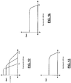
- FIGs. 12 and 13 graphs illustrating characteristic gain-bandwidth curves for a zero-order TIA and a first-order nested TIA, respectively, are shown.
- the gain A defined as the output voltage ⁇ v o divided by the input voltage ⁇ v i , is typically on the order of a few hundred or a few thousand (i.e., approximately 10 2 - 10 3 ).
- a typical range of threshold frequency (f T ) values for a 0.13 ⁇ m CMOS process is 30 GHz - 40 GHz.
- a high gain value yields a bandwidth value of approximately 1 GHz.
- a medium gain value increases the bandwidth to approximately 2 GHz.
- Other values of gain and bandwidth are possible.
- a TIA may have a characteristic gain value that is higher than the maximum shown in FIG. 12 and a bandwidth that is less than 1 GHz.
- a TIA may have a characteristic gain value that is lower than the minimum gain value shown in FIG. 12 and a bandwidth that is greater than 2 GHz.
- the bandwidth varies as an inverse function of gain. This function may be referred to as the "spread". The spread is greater for TIAs using MOS transistors than for TIAs using bipolar junction transistors (BJTs).
- BJTs bipolar junction transistors
- exemplary bandwidth values shown in FIG. 12 do not define upper and lower bandwidth bounds. In many practical applications, bandwidths on the order of 1 GHz or 2 GHz are too low. Many applications, such as an OC192 fiber optic receiver, require bandwidths on the order of 10 GHz. Preamplifiers for high-speed hard disk drives also typically require bandwidths that are on the order of several GHz. Referring now to FIG. 13 , a first-order nested TIA at a typical gain value may have a bandwidth of approximately 10 GHz.
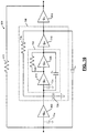
- a second-order nested TIA 800 builds upon the first-order nested TIA 700. Reference numbers from FIGs. 4 and 7 are used in FIG. 8 to identify similar elements.
- the second-order nested TIA 800 includes an opamp 805 at the input of the first-order nested TIA 700 and an opamp 810 at the output of the first-order nested TIA 700.
- An additional feedback resistor 815 is also added across the input of the opamp 805 and the output of the opamp 810.
- An exemplary gain-bandwidth curve that is produced using the second-order nested TIA 800 is shown in FIG. 14 . For a typical gain value, a bandwidth of approximately 20 GHz may be achieved.
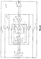
- higher-order nested TIAs may be constructed by adding additional opamps and feedback resistors. Reference numbers from FIGs. 4 , 7 and 8 are used in FIG. 9 to identify similar elements.
- a third-order nested TIA 900 includes opamps 905 and 910 and feedback resistor 915. It is possible to achieve higher values of either gain or bandwidth (or both) by repeating the technique of the present invention. However, the efficiency of the circuit decreases as additional nesting levels are added due to parasitic noise and increased power dissipation. In general, either the first-order nested TIA or the second-order nested TIA will usually provide sufficient performance.
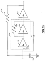
- FIG. 10 a differential mode first-order nested TIA 1000 is shown. Reference numbers from FIG. 5 are used in FIG. 10 to identify similar elements.
- An opamp 1002 is connected to the outputs of the opamp 504.
- Feedback resistors 1006 and 1008 are connected to inputs of the differential mode TIA 500 and to outputs of the opamp 1002. The gain-bandwidth product of the TIA is increased.
- a differential mode nth-order nested TIA 1100 is constructed in a manner that is similar to the nth-order nested TIA of FIG. 9 .
- Reference numbers from FIGs. 5 and 10 are used in FIG. 11 to identify similar elements.
- Additional opamps 1104 and 1108 and feedback resistors 1112 and 1114 are connected in a similar manner.
- the gain-bandwidth characteristics for differential mode TIAs are substantially similar to the gain-bandwidth characteristics shown in FIGs. 12-14 .
- the opamps used in the nested TIA may employ either bipolar junction transistors (BJTs), such as gallium-arsenide (GaAs) transistors, or metal-oxide-semiconductor (MOS) transistors, such as CMOS or BICMOS transistors.
- BJTs bipolar junction transistors
- GaAs gallium-arsenide
- MOS metal-oxide-semiconductor
- CMOS complementary metal-oxide-semiconductor
- the preferred embodiments of the invention use MOS transistors due to practical considerations such as ease of manufacture and better power consumption characteristics.
- the first order nested TIA 700 is shown with additional feedback capacitance C 1 , which substantially cancels effects of an input capacitance C P1 at the input of the opamp 415.
- the feedback capacitance C 1 has a first end that communicates with an input of the opamp 415 and a second end that communicates with an output of the opamp 425.
- the feedback capacitance C 1 has a first end that communicates with an input of the opamp 415 and a second end that communicates with an output of the opamp 425.
- the feedback capacitance C 2 has a first end that communicates with an input of the opamp 805 and a second end that communicates with an output of the opamp 710.
- the feedback capacitance C N has a first end that communicates with an input of the opamp 905 and a second end that communicates with an output of the opamp 810.
- the first order nested differential mode TIA 1000 is shown with additional feedback capacitors C 1A and C 1B , which substantially cancel effects of input parasitic capacitances C P1 and C P2 at the inputs of the differential mode opamp 502.
- the feedback capacitance C 1A has a first end that communicates with an input of the differential mode opamp 502 and a second end that communicates with an output of the differential mode opamp 504.
- additional capacitances C 2A and C 2B are added to a second order differential mode TIAs in a similar manner to offset parasitic capacitances C P2A and C P2B .
- Higher order circuits Use a similar approach.
- the feedback resistance 2010 has a first end that communicates with an input of the opamp 710. A second end of the resistance 2010 communicates with an output of the opamp 710.
- the feedback resistance 2110 has a first end that communicates with an input of the opamp 810. A second end of the resistance 2110 communicates with an output of the opamp 810.
- the feedback resistance 2210 has a first end that communicates with an input of the opamp 710. A second end of the resistance 2210 communicates with an output of the opamp 710.
- the input capacitance C IN has a first end that receives an input signal for the nested TIA 700 and a second end that communicates with an input of opamp 415.
- the feedback capacitance C FB has a first end that communicates with an input of opamp 415 and a second end that communicates with one end of resistance 715.
- the additional feedback resistances, input capacitances, and/or feedback capacitances can also be added to the differential mode nested TIA.
- FIG. 24 the first order differential mode nested TIA of FIG. 10 is shown with first and second input capacitances C IN1 and C IN2 , first and second feedback capacitances C FB1 and C FB2 , and feedback resistances 2410 and 2412.
- the input capacitances C IN1 and C IN2 have first ends that receive input signals for the nested differential mode TIA and second ends that communicate with inputs of opamp 502.
- the feedback capacitances C FB1 and C FB2 have first ends that communicate with inputs of opamp 502 and second ends that communicate with first ends of resistances 1006 and 1008, respectively.
- First and second feedback resistances 2410 and 2412 have first ends that are connected to inputs and second ends that are connected to outputs of differential mode opamp 1002.
- the feedback capacitances ( FIG.s 15-19 ), feedback resistances ( FIGs. 20-24 ), and input and feedback capacitances ( FIGs. 23 and 24 ) can be used in any combination on first, second, ... or n th order nested TIA and/or differential mode TIA.
- an exemplary disk drive system 2500 is shown to include a disk drive write circuit 2510 that writes to a disk drive 2514.
- a disk drive read circuit 2516 includes a preamp circuit 2518 with a nested TIA or nested differential mode TIA identified at 2520, which is implemented as described above.
- Opamp 710 includes a first transistor 2600 in series with a second transistor 2602. A gate of the first transistor 2600 is driven by the output of the zero-order TIA 705. A gate of the second transistor 2602 is driven by a bias voltage V B .
- the signal output of TIA 700 is taken at a node connecting a source of the first transistor 2600 with a drain of the second transistor 2602.
- a first current source 2604 draws current from a source of the second transistor 2602.
- the opamp 710 can be powered with a drain supply voltage V dd2 . Power supply options are described below in more detail.
- Opamp 1002 includes a first transistor 2700 in communication with a second transistor 2702.
- a gate of the first transistor 2700 is driven by one output of the differential zero-order TIA 500.
- a gate of the second transistor 2702 is driven by a bias voltage V B .
- a first signal output of TIA 1000 is taken at a node connecting a source of the first transistor 2600 with a drain of the second transistor 2702.
- a first current source 2704 draws current from a source of the second transistor 2702.
- a third transistor 2706 is in communication with a fourth transistor 2708.
- a gate of the third transistor 2706 is driven by the other output of the differential zero-order TIA 500.
- a gate of the fourth transistor 2708 is driven by V B .
- a second signal output of TIA 1000 is taken at a node connecting a source of the third transistor 2706 with a drain of the fourth transistor 2708.
- a second current source 2710 draws current from a source of the second transistor 2702.
- the opamp 1002 can be powered with a drain supply voltage V dd2 . Power supply options are described below in more detail.
- the differential signal output is taken across the first and second signal outputs at the respective sources of first and third transistors 2700, 2706.
- the first-order nested TIA 700 of FIG. 26 is shown including a second implementation of opamp 710.
- the second implementation includes a second current source 2610 that provides current to the drain of the first transistor 2600.
- the second current source 2610 draws current from V dd2 .
- the differential mode first-order nested TIA 1000 of FIG. 27 is shown including a second implementation of opamp 1002.
- the second implementation includes a third current source 2712 that provides current to the drains of first transistor 2700 and third transistor 2706.
- the third current source 2712 draws current from V dd2 .
- Opamp 1002 includes a push-pull configuration as shown.
- the opamp 1002 receives a positive bias voltage V BP and a negative bias voltage V BN .
- the differential output signal is taken across nodes V out+ and V out- .
- the gain curves represent typical gain patterns of the various first-order nested TIAs described above.
- a logarithmic horizontal axis of each graph represents signal frequency.
- the graph of FIG. 31 represents a gain curve 3100 of the various opamps.
- the opamps provide a lower gain and higher bandwidth than the zero-order TIAs.
- the opamp gain rolls off at a rate of 20dB/decade.
- the graph of FIG. 32 represents a family of gain curves 3200 for various TIAs.
- the gain curve 3200 having the smallest bandwidth corresponds with a zero-order TIA.
- the gain curves 3200 with higher bandwidths correspond with increasingly-nested TIAs.
- the TIAs generally provide a high gain and medium bandwidth when compared to the opamps.
- the zero-order TIA gain rolls off at a rate of 20dB/decade.
- the graph of FIG. 33 represents a family of gain curves 3300 of the various first-order nested TIAs.
- the gains are relatively flat at the lowest frequencies. As the frequency increases the gains roll off at 20dB/decade due to the gain effects of the opamp as shown in FIG. 31 . As the frequency continues to increase the gains roll off at 40dB/decade due to the combined effects of the opamp and the selected zero-order TIA.
- FIG. 34 a functional block diagram is shown of a power supply arrangement for first-order nested TIAs.
- the power supply arrangement provides a TIA chip with three unique voltages levels despite providing external connections for two voltages and ground. While FIG. 34 shows the power supply connected to the first-order nested TIA 700 of FIG. 7 , it is understood by those skilled in the art that the power supply may be used with other single-ended and differential first-order nested TIAs.
- An analog power supply V dda is associated with one of the external connections and provides power to the zero-order TIA. In some examples V dda is between about 2.5V and 3.3V.
- the analog power supply V dda also provides power to a charge pump module 3400.
- Charge pump module 3400 also receives power from a digital power supply V ddd .
- V ddd is associated with the second one of the external connections.
- Charge pump module 3400 can be fabricated on the same chip as the first-order nested TIAs. In some examples V ddd is about 1.2V. In some embodiments V ddd can be regulated by a voltage regulator module 3402 before being applied to the charge pump module 3400.
- the charge pump module 3400 generates a second digital voltage V dd2 that is approximately equal to V dda +V ddd . Therefore V dd2 >V dda . It is appreciated by those skilled in the art that V dd2 is not exactly equal to V dda +V ddd due to losses and/or inefficiencies inherent in the charge pump module 3400.
- V dda is provided by a battery 3500.
- Battery 3500 can be a lithium-ion battery having a voltage between about 2.7V and 4.2V.
- a light-emitting diode (LED) communicates with an output of the opamp 710. In some embodiments the LED has a turn-on voltage V D of about 3.5V.
- the charge pump module 3400 adds V dda from the battery 3500 to V ddd to generate sufficient voltage for driving the LED 3502. Since V ddd generally provides only about 1.2V it can not be used alone to power the LED 3502.
- the charge pump module 3400 provides the additional voltage from V dda to supply the LED with approximately 3.7V to 4.2V, which is above the 3.5V V D .
- the range of 3.7V to 4.2V accounts for the losses and/or inefficiencies in the charge pump module 3400 and is therefore not exactly equal to V dda +V ddd .
- the present disclosure also addresses the need for increasing the gain-bandwidth product of TIAs. Improvements in the gain-bandwidth product may be achievable by "nesting" a TIA within another TIA. In other words, additional circuit elements such as feedback resistances, capacitances and/or opamps are added on the input and/or output sides of the TIA.
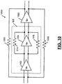
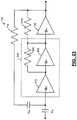
- the transimpedance amplifier 3602 includes a first operational amplifier 3604 and a second operational amplifier 3606. Each operational amplifier set forth in this figure and the following figures has a non-inverting input and non-inverting output identified by the absence of the "o" symbol, and an inverting input and inverting output identified by the "o" symbol.
- the transimpedance amplifier 3602 also includes a first feedback resistance 3608 that communicates with the non-inverting input and the inverting output, and a second resistance 3610 that communicates with the inverting input and the non-inverting output.
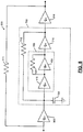
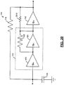
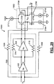
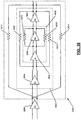
- the nested transimpedance amplifier 3600 also includes a third operational amplifier 3612 also having an inverting input and output, and a non-inverting input and output.
- the operational amplifier 3612 has an inverting output that communicates with the non-inverting input of amplifier 3606, and a non-inverting output that communicates with the inverting input of amplifier 3606.
- a feedback resistance 3614 communicates with the non-inverting output of amplifier 3612 and the inverting output of amplifier 3604.
- the inverting output of amplifier 3612 communicates with the non-inverting output of amplifier 3604. That is, resistance 3614 communicates with the inverting input of amplifier 3606, while resistance 3616 communicates with the non-inverting input of amplifier 3606.
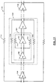
- the double-nested transimpedance amplifier includes the transimpedance amplifier 3602 and the nested transimpedance amplifier structure 3600 of FIG. 36 . Therefore, these common circuit components will not be described further.
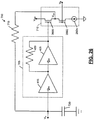
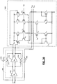
- another amplifier 3702 also having inverting and non-inverting inputs and outputs is illustrated.
- the inverting output of amplifier 3702 communicates with the non-inverting input of amplifier 3612.
- the non-inverting output of amplifier 3702 communicates with the inverting input of amplifier 3612.
- a feedback resistance 3704 communicates with the common node of the inverting output of amplifier 3702 and the non-inverting input of amplifier 3612.
- the resistance 3704 is also communicates with the inverting output of amplifier 3604.
- a second feedback resistance 3705 communicates with the common node between the non-inverting output of amplifier 3702 and the inverting input of amplifier 3612, and the non-inverting output of amplifier 3604.
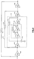
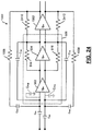
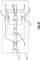
- a transimpedance structure 3602 illustrated in FIG. 36 is used in a nested TIA 3800.
- an operational amplifier 3802 has its inverting input connected to the non-inverting output of amplifier 3604.
- the non-inverting input of amplifier 3802 is connected to the inverting output of amplifier 3604.
- Another amplifier 3804 has an inverting output that is connected to the non-inverting input of amplifier 3606.
- the non-inverting output of amplifier 3804 connected to the inverting input of amplifier 3606.
- Another operational amplifier 3806 has an inverting output that is connected to the non-inverting input of amplifier 3804 and a non-inverting output that is connected to the inverting input of amplifier 3804.
- a first feedback resistance 3808 is connected to the common node between the inverting output of amplifier 3804 and the non-inverting input of amplifier 3606, and the inverting output of amplifier 3802.
- Another feedback resistance 3810 is connected to the common node of the non-inverting output of amplifier 3804 and the inverting input of amplifier 3606, and the non-inverting output of amplifier 3802.
- a feedback resistance 3812 is connected to the common node between the non-inverting output of amplifier 3806 and the inverting amplifier 3804, and the inverting output of amplifier 3802.
- Another resistance 3814 is connected to the node between inverting output of amplifier 3806 and the non-inverting input of amplifier 3804, and the non-inverting output of 3802.
- the amplifier 3802 is not important as far as nesting is concerned. If the input of the circuit is current instead of voltage, amplifier 3806 may not be required.
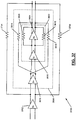
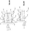
- FIGs. 39A and 39B differential and single-ended transimpedance amplifiers having capacitive feedback are shown, respectively.
- a differential transimpedance amplifier 3900 which is similar to the transimpedance amplifier 3602 of FIG. 36 , is illustrated having a first capacitance 3902 in parallel with resistance 3608 and a second capacitance 3904 in parallel with resistance 3610.
- the frequency response or the stability of the transimpedance network may be improved by including the capacitances 3902 and 3904.
- the capacitances can be replaced by inductances if desired.
- FIG. 39B a single-ended transimpedance amplifier 3900' is shown that is similar to the differential configuration shown in FIG. 39A .
- similar elements are labeled with a prime symbol "'".
- the transconductance g m of the amplifiers 3604' and/or 3606' may be negative and/or the signals may be coupled to inverting input(s) of the amplifiers 3604' and/or 3606'.
- FIG. 40A a differential transimpedance amplifier 4000 is shown.
- a first operational amplifier 4002 has a non-inverting input communicates with an inverting output of amplifier 4004.
- the inverting input of amplifier 4002 communicates with the non-inverting output of amplifier 4004.
- a feedback element 4006 communicates with the common node of the non-inverting input of amplifier 4002 and the inverting output of amplifier 4004, and the inverting output of amplifier 4002.
- a second feedback element 4008 communicates with the common node of the inverting input of amplifier 4002 and the non-inverting output of amplifier 4004, and the non-inverting output of amplifier 4002.
- the feedback element 4006 includes a resistance 4010, a series combination of a resistance 4012, and an inductance 4014.
- the inductance 4014 can be a variable inductance.
- a variable capacitance 4016 is coupled in parallel with the series combination of the resistance 4012 and the inductance 4014. This parallel combination is coupled in series with the resistance 4010.
- the feedback element 4008 is configured in a similar way with a resistance 4020, a second resistance 4022 in series with an inductance 4024, and a variable capacitance 4026.
- variable capacitances 4016 and 4026 are used to illustrate that various resonant frequencies of the LC tank circuit may be adjusted by changing the capacitance values.
- a fixed capacitance set to the desired residence frequency may be used.
- the circuit 4000 may be suitable for use as an RF amplifier in a TV tuner in which it is desirable to include an ultra-wide band of operation (e.g., 50 MHz-1 GHz).
- the circuit amplifies the wanted signal more than the unwanted signal by taking advantage of the LC tank in combination with the transimpedance amplifier property of the wide-band operation.
- the parallel LC tank circuit causes the feedback network to have high impedance at a resonance frequency of the LC tank circuit.
- the structure illustrated in FIG. 40 may also be nested in an amplifier structure illustrated above. With each subsequent nesting, only the signal frequency of interest is amplified so that the nesting behavior is effective at the residence frequency of the LC tank elements. Because of this, the selectivity of the nested LC tank circuit transimpedance amplifier is significantly improved while the out-of-band signals are not amplified. This improves the distortion performance of the amplifier by not amplifying the unwanted signals. At the same time, in-band signals are amplified with extremely low distortion because of the nature of the nesting transimpedance amplifier.
- FIG. 40B a single-ended transimpedance amplifier 4000' is shown that is similar to the differential configuration shown in FIG. 40A .
- similar elements are labeled with a prime symbol "'".
- the transconductance g m of the amplifiers 4002' and/or 4004' may be negative and/or the signals may be coupled to inverting input(s) of the amplifiers 4002' and/or 4004'.
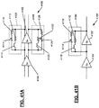
- FIG. 41A a differential transimpedance amplifier 4100 using an LC circuit is illustrated.
- a first operational amplifier 4102 communicates with a second amplifier 4104.
- An inverting output of amplifier 4104 communicates with a non-inverting input of amplifier 4102.
- a non-inverting output of amplifier 4104 communicates with an inverting input of amplifier 4102.
- a first LC circuit 4106 communicates with the non-inverting input of amplifier 4102 and the inverting output of amplifier 4102.
- a second LC circuit 4108 communicates with the inverting input and the non-inverting output of amplifier 4102.
- LC circuit 4106 includes an inductance 4110 in series with a resistance 4112.
- the LC circuit 4106 also includes a capacitance 4114 in series with a resistance 4116.
- the series combination of the capacitance 4114 and resistance 4116 is in parallel with the series combination of the inductance 4110 and the resistance 4112.
- the LC circuit 4108 is configured in a similar manner to LC circuit 4106.
- the LC circuit 4108 includes an inductance 4120 in series with a resistance 4122.
- a capacitance 4124 is in series with a resistance 4126.
- the series combination of the inductance 4120 and resistance 4122 is in parallel with the series combination of the capacitance 4124 and the resistance 4126.
- FIG. 41B a single-ended transimpedance amplifier 4100' is shown that is similar to the differential configuration shown in FIG. 41A .
- similar elements are labeled with a prime symbol "'".
- the transconductance g m of the amplifiers 4102' and/or 4104' may be negative and/or the signals may be coupled to inverting input(s) of the amplifiers 4102' and/or 4104'.
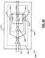
- FIG. 42 an integrator 4200 that is formed using a nested transimpedance amplifier is illustrated. This example is identical to the double-nested transimpedance amplifier illustrated in FIG. 37 , except that resistances 3704 and 3705 have been replaced with capacitances 4202 and 4204.
- the integrator 4200 has a high bandwidth due to the transimpedance configuration.
- the impedance output is low even at high frequencies. Because of the low output impedance, the integrator 4200 may be useful to drive large capacitive loads.
- One application of the integrator 4200 may be in a Sigma-Delta analog-to-digital converter that operates at gigahertz over sampling frequencies.
- the present disclosure can be implemented in amplifiers and/or integrators of a hard disk drive 4300.
- the present disclosure may implement and/or be implemented in either or both signal processing and/or control circuits and/or a power supply 4303, which are generally identified in FIG. 43A at 4302.
- the signal processing and/or control circuit 4302 and/or other circuits (not shown) in the HDD 4300 may process data, perform coding and/or encryption, perform calculations, and/or format data that is output to and/or received from a magnetic storage medium 4306.
- the HDD 4300 may communicate with a host device (not shown) such as a computer, mobile computing devices such as personal digital assistants, cellular phones, media or MP3 players and the like, and/or other devices via one or more wired or wireless communication links 4308.
- a host device such as a computer, mobile computing devices such as personal digital assistants, cellular phones, media or MP3 players and the like, and/or other devices via one or more wired or wireless communication links 4308.
- the HDD 4300 may be connected to memory 4309 such as random access memory (RAM), low latency nonvolatile memory such as flash memory, read only memory (ROM) and/or other suitable electronic data storage.
- RAM random access memory
- ROM read only memory
- the present disclosure can be implemented in amplifiers and/or integrators of a digital versatile disc (DVD) drive 4310.
- the present disclosure may implement and/or be implemented in either or both signal processing and/or control circuits, which are generally identified in FIG. 43B at 4312, mass data storage of the DVD drive 4310 and/or a power supply 4313.
- the signal processing and/or control circuit 4312 and/or other circuits (not shown) in the DVD 4310 may process data, perform coding and/or encryption, perform calculations, and/or format data that is read from and/or data written to an optical storage medium 4316.
- the signal processing and/or control circuit 4312 and/or other circuits (not shown) in the DVD 4310 can also perform other functions such as encoding and/or decoding and/or any other signal processing functions associated with a DVD drive.
- the DVD drive 4310 may communicate with an output device (not shown) such as a computer, television or other device via one or more wired or wireless communication links 4317.
- the DVD 4310 may communicate with mass data storage 4318 that stores data in a nonvolatile manner.
- the mass data storage 4318 may include a hard disk drive (HDD).
- the HDD may have the configuration shown in FIG. 43A .
- the HDD may be a mini HDD that includes one or more platters having a diameter that is smaller than approximately 1.8".
- the DVD 4310 may be connected to memory 4319 such as RAM, ROM, low latency nonvolatile memory such as flash memory and/or other suitable electronic data storage.
- the present disclosure can be implemented in amplifiers and/or integrators of a high definition television (HDTV) 4320.
- the present disclosure may implement and/or be implemented in either or both signal processing and/or control circuits, which are generally identified in FIG. 43E at 4322, a WLAN interface, mass data storage of the HDTV 4320 and/or a power supply 4323.
- the HDTV 4320 receives HDTV input signals in either a wired or wireless format and generates HDTV output signals for a display 4326.
- signal processing circuit and/or control circuit 4322 and/or other circuits (not shown) of the HDTV 4320 may process data, perform coding and/or encryption, perform calculations, format data and/or perform any other type of HDTV processing that may be required.
- the HDTV 4320 may communicate with mass data storage 4327 that stores data in a nonvolatile manner such as optical and/or magnetic storage devices. At least one HDD may have the configuration shown in FIG. 43A and/or at least one DVD may have the configuration shown in FIG. 43B .
- the HDD may be a mini HDD that includes one or more platters having a diameter that is smaller than approximately 1.8".
- the HDTV 4320 may be connected to memory 4328 such as RAM, ROM, low latency nonvolatile memory such as flash memory and/or other suitable electronic data storage.
- the HDTV 4320 also may support connections with a WLAN via a WLAN network interface 4329.
- the present disclosure may implement and/or be implemented in amplifiers and/or integrators of a control system of a vehicle 4330, a WLAN interface, mass data storage of the vehicle control system and/or a power supply 4333.
- the present disclosure implement a powertrain control system 4332 that receives inputs from one or more sensors such as temperature sensors, pressure sensors, rotational sensors, airflow sensors and/or any other suitable sensors and/or that generates one or more output control signals such as engine operating parameters, transmission operating parameters, and/or other control signals.
- the present disclosure may also be implemented in other control systems 4340 of the vehicle 4330.
- the control system 4340 may likewise receive signals from input sensors 4342 and/or output control signals to one or more output devices 4344.
- the control system 4340 may be part of an anti-lock braking system (ABS), a navigation system, a telematics system, a vehicle telematics system, a lane departure system, an adaptive cruise control system, a vehicle entertainment system such as a stereo, DVD, compact disc and the like. Still other implementations are contemplated.
- the powertrain control system 4332 may communicate with mass data storage 4346 that stores data in a nonvolatile manner.
- the mass data storage 4346 may include optical and/or magnetic storage devices for example hard disk drives HDD and/or DVDs. At least one HDD may have the configuration shown in FIG. 43A and/or at least one DVD may have the configuration shown in FIG. 43B .
- the HDD may be a mini HDD that includes one or more platters having a diameter that is smaller than approximately 1.8".
- the powertrain control system 4332 may be connected to memory 4347 such as RAM, ROM, low latency nonvolatile memory such as flash memory and/or other suitable electronic data storage.
- the powertrain control system 4332 also may support connections with a WLAN via a WLAN network interface 4348.
- the control system 4340 may also include mass data storage, memory and/or a WLAN interface (all not shown).
- the present disclosure can be implemented in amplifiers and/or integrators of a cellular phone 4350 that may include a cellular antenna 4351.
- the present disclosure may implement and/or be implemented in either or both signal processing and/or control circuits, which are generally identified in FIG. 43E at 4352, a WLAN interface, mass data storage of the cellular phone 4350 and/or a power supply 4353.
- the cellular phone 4350 includes a microphone 4356, an audio output 4358 such as a speaker and/or audio output jack, a display 4360 and/or an input device 4362 such as a keypad, pointing device, voice actuation and/or other input device.
- the signal processing and/or control circuits 4352 and/or other circuits (not shown) in the cellular phone 4350 may process data, perform coding and/or encryption, perform calculations, format data and/or perform other cellular phone functions.
- the cellular phone 4350 may communicate with mass data storage 4364 that stores data in a nonvolatile manner such as optical and/or magnetic storage devices for example hard disk drives HDD and/or DVDs. At least one HDD may have the configuration shown in FIG. 43A and/or at least one DVD may have the configuration shown in FIG. 43B .
- the HDD may be a mini HDD that includes one or more platters having a diameter that is smaller than approximately 1.8".
- the cellular phone 4350 may be connected to memory 4366 such as RAM, ROM, low latency nonvolatile memory such as flash memory and/or other suitable electronic data storage.
- the cellular phone 4350 also may support connections with a WLAN via a WLAN network interface 4368.
- the present disclosure can be implemented in amplifiers and/or integrators of a set top box 4380.
- the present disclosure may implement and/or be implemented in either or both signal processing and/or control circuits, which are generally identified in FIG. 43F at 4384, a WLAN interface, mass data storage of the set top box 4380 and/or a power supply 4383.
- the set top box 4380 receives signals from a source such as a broadband source and outputs standard and/or high definition audio/video signals suitable for a display 4388 such as a television and/or monitor and/or other video and/or audio output devices.
- the signal processing and/or control circuits 4384 and/or other circuits (not shown) of the set top box 4380 may process data, perform coding and/or encryption, perform calculations, format data and/or perform any other set top box function.
- the set top box 4380 may communicate with mass data storage 4390 that stores data in a nonvolatile manner.
- the mass data storage 4390 may include optical and/or magnetic storage devices for example hard disk drives HDD and/or DVDs. At least one HDD may have the configuration shown in FIG. 43A and/or at least one DVD may have the configuration shown in FIG. 43B .
- the HDD may be a mini HDD that includes one or more platters having a diameter that is smaller than approximately 1.8".
- the set top box 4380 may be connected to memory 4394 such as RAM, ROM, low latency nonvolatile memory such as flash memory and/or other suitable electronic data storage.
- the set top box 4380 also may support connections with a WLAN via a WLAN network interface 4396.
- the present disclosure can be implemented in amplifiers and/or integrators of a media player 4400.
- the present disclosure may implement and/or be implemented in either or both signal processing and/or control circuits, which are generally identified in FIG. 43G at 4404, a WLAN interface, mass data storage of the media player 4400 and/or a power supply 4403.
- the media player 4400 includes a display 4407 and/or a user input 4408 such as a keypad, touchpad and the like.
- the media player 4400 may employ a graphical user interface (GUI) that typically employs menus, drop down menus, icons and/or a point-and-click interface via the display 4407 and/or user input 4408.
- GUI graphical user interface
- the media player 4400 further includes an audio output 4409 such as a speaker and/or audio output jack.
- the signal processing and/or control circuits 4404 and/or other circuits (not shown) of the media player 4400 may process data, perform coding and/or encryption, perform calculations, format data and/or perform any other media player function.
- the media player 4400 may communicate with mass data storage 4410 that stores data such as compressed audio and/or video content in a nonvolatile manner.
- the compressed audio files include files that are compliant with MP3 format or other suitable compressed audio and/or video formats.
- the mass data storage may include optical and/or magnetic storage devices for example hard disk drives HDD and/or DVDs. At least one HDD may have the configuration shown in FIG. 43A and/or at least one DVD may have the configuration shown in FIG. 43B .
- the HDD may be a mini HDD that includes one or more platters having a diameter that is smaller than approximately 1.8".
- the media player 4400 may be connected to memory 4414 such as RAM, ROM, low latency nonvolatile memory such as flash memory and/or other suitable electronic data storage.
- the media player 4400 also may support connections with a WLAN via a WLAN network interface 4416. Still other implementations in addition to those described above are contemplated.
- the Sigma Delta ADC module 2810 includes a difference amplifier module 4514 that receives an analog input signal.
- An output of the difference amplifier module 4514 is input to an integrator module 4518.
- An output of the integrator module 4518 is one input of a comparator module 4520.
- Another input of the comparator module 4520 may be connected to a reference potential such as ground.
- An output of the comparator module 4520 is input to a filter and decimator module 4524, which outputs a digital signal.
- the output of the comparator module 4520 is input to a digital to analog converter (DAC) module 4528.
- the DAC module 4528 may be a 1-bit DAC.
- An output of the DAC module 4528 is input to an inverting input of the difference amplifier module 4514.
- the output of the DAC module 4528 is subtracted from the input signal.
- the resulting signal is integrated by the integrator module 4518.
- the integrator output voltage is converted to a single bit digital output (1 or 0) by the comparator module 4520.
- the resulting bit becomes an input to the DAC module 4528.
- This closed-loop process may be carried out at a very high oversampled rate.
- the digital data output by the comparator module is a stream of ones and zeros and the value of the signal is proportional to the density of ones output by the comparator module. For an increasing value, the density of ones increases. For a decreasing value, the density of ones decreases.
- the integrator acts as a lowpass filter to the input signal and a highpass filter to the quantization noise.
- the bit stream is digitally filtered by the filter and decimator module to provide a binary-format output.
- the TIA amplifiers described in the embodiments set forth above may be used to implement one or more of the difference amplifier module, the integrator module and the comparator module in the Sigma Delta DAC module.
Description
- This application is a continuation of United States Patent Application No.
11/495,813, filed July 28, 2006 U.S. Provisional Application No. 60/817,268, filed on June 29, 2006 60/798,480, filed May 8, 2006 60/798,567, filed on May 8, 2006 60/759,899, filed on January 18, 2006 10/459,731 filed on June 11, 2003 6,762,644 issued on July 13, 2004 , which claims the benefit ofU.S. Provisional Application No. 60/275,109, filed March 13, 2001 - The present invention relates to transimpedance amplifiers, and more particularly to nested transimpedance amplifiers with an increased gain-bandwidth product.
- A transimpedance amplifier (TIA) is a well-known type of electronic circuit. Referring now to
FIG. 1 , a TIA 100 includes an operational amplifier (opamp) 105 having a gain parameter (-gm). Theopamp 105 is connected in parallel to a resistor (Rf) 110. The input to the TIA 100 is a current (Δi) 115. The output of theTIA 100 is a voltage (Δvo) 120. - Referring now to
FIG. 2 , theopamp 105 of the TIA 100 is replaced by acurrent source 205 and atransistor 210 having gain -gm. The TIA 100 inFIGs. 1 and 2 is often referred to as a transconductance amplifier because it converts the input current Δi into the output voltage Δvo. - Referring now to
FIG. 3 , a TIA 300 converts an input voltage (Δvi) 305 into an output voltage (Δvo) 310. The TIA 300 also includes aresistor 315 that is connected to atransistor 320. The TIA 300 is typically used in applications that require relatively low bandwidth. - Referring now to
FIG. 4 , a TIA 400 converts an input voltage (Δvi) 405 into an output voltage (Δvo) 410. The TIA 400 includes asecond opamp 415, which is connected in series to a parallel combination of a resistor (Rf) 420 and anopamp 425. The TIA 400 is typically used for applications having higher bandwidth requirements than the TIA 300. - Ordinarily, the bandwidth of the TIA is limited to a fraction of a threshold frequency fT of transistor(s) that are used in the opamp(s). In the case of a bipolar junction transistor (BJT) such as a gallium-arsenide (GaAs) transistor, the bandwidth of the TIA is approximately equal to 10%-20% of fT. For metal-oxide-semiconductor (MOS) transistors), the bandwidth of the TIA is typically a few percent (i.e., approximately 2%-6%) of fT.
- Referring now to
FIG. 5 , a TIA 500 may be configured to operate differentially using two inputs of eachopamp input 505 acts as a reference, in a similar manner as ground or virtual ground in a standard configuration TIA. The input voltage Δvi and the output voltage Δvo are measured as voltage differences between areference input 505 and asecond input 510.Feedback resistors opamp 504. - Referring now to
FIG. 6 , one TIA application having a relatively high bandwidth requirement is that of an optical sensor. Anoptical sensor circuit 600 includes theopamp 105 and theresistor 110 of the TIA 100 that are coupled with aphotodiode 605. The output of thephotodiode 605 is acurrent I photo 610, which acts as an input to the TIA 100. - The patent publication
US6,762,644 B1 discloses an alternative nested TIA. - Increasingly, applications require both high bandwidth and high gain. Examples include optical sensors, such as fiber optic receivers, and preamplifier writers for high-speed hard disk drives.
- A differential transimpedance amplifier circuit comprises a first operational amplifier having a first inverting input, a first non-inverting input, a first inverting output and a first non-inverting output; a second operational amplifier having a second inverting input, a second non-inverting input, a second inverting output and a second non-inverting output, wherein the second inverting output is connected to the first non-inverting input and the second non-inverting output is connected to the first inverting input; a third operational amplifier having a third inverting input, a third non-inverting input, a third inverting output and a third non-inverting output, wherein the second inverting input is connected to the third non-inverting output and the second non-inverting input is connected to the third inverting output; a fourth operational amplifier having a fourth inverting input, a fourth non-inverting input, a fourth inverting output and a fourth non-inverting output, wherein the fourth inverting output is connected to the third non-inverting input and the fourth non-inverting output is connected to the third inverting input; a first feedback element that is connected to the second non-inverting input and the second inverting output; a second feedback element that is connected to the second inverting input and the second non-inverting output; a third feedback element that is connected to the third non-inverting input and the first inverting output; a fourth feedback element that is connected to the third inverting input and the first non-inverting output; a fifth feedback element that is connected to the fourth inverting input and the first inverting output; and a sixth feedback element that is connected to the fourth non-inverting output and the first non-inverting output.
- In other features, the first and second feedback elements comprise first and second resistances, respectively. The third and fourth feedback elements comprise first and second resistances, respectively. The fifth and sixth feedback elements comprise first and second resistances, respectively.
- A Sigma-Delta analog to digital converter comprises the differential transimpedance amplifier.
- Further areas of applicability of the present invention will become apparent from the detailed description provided hereinafter. It should be understood that the detailed description and specific examples, while indicating the preferred embodiment of the invention, are intended for purposes of illustration only and are not intended to limit the scope of the invention.
- The present invention will become more fully understood from the detailed description and the accompanying drawings, wherein:
-
FIGs. 1 and 2 are basic circuit architectures for a current-to-voltage TIA according to the prior art; -
FIGs. 3 and 4 are basic circuit architectures for a voltage-to-voltage TIA according to the prior art; -
FIG. 5 is a basic circuit architecture for a differential configuration of a TIA according to the prior art; -
FIG. 6 shows an optical sensor, including a photodiode coupled to a TIA, according to the prior art; -
FIG. 7 is a first-order nested TIA; -
FIG. 8 is a second-order nested TIA; -
FIG. 9 is an nth-order nested TIA; -
FIG. 10 is a first-order nested TIA in a differential configuration; -
FIG. 11 is an nth-order nested TIA in a differential configuration; -
FIG. 12 is a graph of exemplary gain-bandwidth characteristics for a TIA; -
FIG. 13 is a graph of an exemplary gain-bandwidth characteristic for a first-order nested TIA; -
FIG. 14 is a graph of an exemplary gain-bandwidth characteristic for a second-order nested TIA; -
FIG. 15 is a first-order nested TIA with capacitive cancellation of input parasitic capacitance; -
FIG. 16 is a second-order nested TIA with capacitive cancellation of input parasitic capacitance; -
FIG. 17 is an nth-order nested TIA with capacitive cancellation of input parasitic capacitance; -
FIG. 18 is a first-order nested TIA in a differential configuration with capacitive cancellation of input parasitic capacitance; -
FIG. 19 is a second order nested TIA in a differential configuration with capacitive cancellation of input parasitic capacitance; -
FIG. 20 illustrates the first order nested TIA ofFIG. 7 with additional feedback resistance; -
FIG. 21 illustrates a second order nested TIA ofFIG. 8 with additional feedback resistance; -
FIG. 22 illustrates the first order nested TIA ofFIG. 15 with additional feedback resistance; -
FIG. 23 illustrates the first order nested TIA ofFIG. 7 with an additional input capacitance, feedback capacitance, and feedback resistance; -
FIG. 24 illustrates the first order differential mode TIA ofFIG. 10 with an additional input capacitance, feedback capacitance, and feedback resistance; -
FIG. 25 illustrates an exemplary disk drive system including a preamplifier with a nested TIA; -
FIG. 26 illustrates the first order nested TIA ofFIG. 7 including an opamp of a first configuration; -
FIG. 27 illustrates the differential first-order nested TIA ofFIG. 10 including an differential opamp of the first configuration; -
FIG. 28 illustrates the first order nested TIA ofFIG. 26 including an opamp of a second configuration; -
FIG. 29 illustrates the differential first-order nested TIA ofFIG. 27 including an differential opamp of the second configuration; -
FIG. 30 illustrates the differential first-order nested TIA ofFIG. 10 including a differential opamp in a push-pull configuration; -
FIGs. 31-33 show a family of gain curves for first and second stages of nested TIAs; -
FIG. 34 shows a functional block diagram of a power supply for nested TIAs; -
FIG. 35 illustrates and exemplary LED drive circuit using the power supply ofFIG. 34 ; -
FIG. 36 is a simplified schematic view of a differential single-nested transimpedance amplifier; -
FIG. 37 is a simplified schematic view of a differential double-nested transimpedance amplifier; -
FIG. 38 is a simplified schematic view of a differential amplifier nested according to a third embodiment of the disclosure; -
FIGs. 39A and 39B are schematic views of differential and single-ended transimpedance amplifiers, respectively, having a compensation capacitor in a feedback loop; -
FIGs. 40A and 40B are schematic views of differential and single-ended nested transimpedance amplifiers, respectively, having an LC tank circuit; - FIGs-41A and 41B are schematic views of differential and single-ended transimpedance amplifiers, respectively, having an LC tank circuit and resistors in the feedback loops;
-
FIG. 42 is a schematic view of an alternative embodiment of a transimpedance amplifier having an LC tank circuit; -
FIG. 43A is a functional block diagram of a hard disk drive; -
FIG. 43B is a functional block diagram of a digital versatile disk (DVD); -
FIG. 43C is a functional block diagram of a high definition television; -
FIG. 43D is a functional block diagram of a vehicle control system; -
FIG. 43E is a functional block diagram of a cellular phone; -
FIG. 43F is a functional block diagram of a set top box; -
FIG. 43G is a functional block diagram of a media player; and -
FIG. 44 is a functional block diagram of a Delta-Sigma analog to digital converter (ADC). - The following description of the preferred embodiment(s) is merely exemplary in nature and is in no way intended to limit the invention, its application, or uses.
- The present invention addresses the need for increasing the gain-bandwidth product of TIAs. Improvements in the gain-bandwidth product are achievable by "nesting" a TIA within another TIA. In other words, additional circuit elements such as feedback resistors, capacitors and/or opamps are added on the input and/or output sides of the TIA. In
FIGs. 15-17 , capacitive cancellation of the input parasitic capacitance is provided. InFIGs. 20-24 , additional feedback resistance is provided. InFIGs. 23 and24 , input and/or feedback capacitance is provided. - Referring now to
FIGs. 7 ,8 , and9 , a "nested" TIA is constructed by adding opamps, feedback resistors and/or capacitors to a zero-order TIA. InFIGs. 10 and11 , a nested TIA may also be constructed to operate in a differential mode. - Referring back to
FIG. 7 , a first-order nestedTIA 700 is shown. Reference numbers fromFIG. 4 are used inFIG. 7 to identify similar elements. TheTIA 700 includes a conventional TIA 705 (also referred to herein as a "zero-order" TIA), anopamp 710, and afeedback resistor 715. Thefeedback resistor 715 may be a standard fixed-value resistor, a nonlinear variable resistor, or an MOS resistor. Acapacitor 720 is also connected between an input of theTIA 700 and ground (or virtual ground). - By nesting the TIA in this manner, improvements in the gain-bandwidth product may be realized. For example, the first-order nested
TIA 700 that uses MOS transistors may achieve a bandwidth that is 10% - 20% of the threshold frequency fT. This range represents a bandwidth that is approximately five to ten times greater than the bandwidth of the corresponding zero-order TIA. - Referring now to
FIGs. 12 and 13 , graphs illustrating characteristic gain-bandwidth curves for a zero-order TIA and a first-order nested TIA, respectively, are shown. In general, a higher value of gain is associated with a lower value of bandwidth, and a lower value of gain is associated with a higher value of bandwidth. The gain A, defined as the output voltage Δvo divided by the input voltage Δvi, is typically on the order of a few hundred or a few thousand (i.e., approximately 102 - 103). A typical range of threshold frequency (fT) values for a 0.13 µm CMOS process is 30 GHz - 40 GHz. - In
FIG. 12 , three exemplary characteristic curves are shown. A high gain value yields a bandwidth value of approximately 1 GHz. A medium gain value increases the bandwidth to approximately 2 GHz. Other values of gain and bandwidth are possible. For example, a TIA may have a characteristic gain value that is higher than the maximum shown inFIG. 12 and a bandwidth that is less than 1 GHz. A TIA may have a characteristic gain value that is lower than the minimum gain value shown inFIG. 12 and a bandwidth that is greater than 2 GHz. As can be appreciated, the bandwidth varies as an inverse function of gain. This function may be referred to as the "spread". The spread is greater for TIAs using MOS transistors than for TIAs using bipolar junction transistors (BJTs). Thus, the need to improve the TIA bandwidth performance is more pronounced with MOS transistors than with BJT transistors. - The exemplary bandwidth values shown in
FIG. 12 do not define upper and lower bandwidth bounds. In many practical applications, bandwidths on the order of 1 GHz or 2 GHz are too low. Many applications, such as an OC192 fiber optic receiver, require bandwidths on the order of 10 GHz. Preamplifiers for high-speed hard disk drives also typically require bandwidths that are on the order of several GHz. Referring now toFIG. 13 , a first-order nested TIA at a typical gain value may have a bandwidth of approximately 10 GHz. - Referring now to
FIG. 8 , a second-order nestedTIA 800 builds upon the first-order nestedTIA 700. Reference numbers fromFIGs. 4 and7 are used inFIG. 8 to identify similar elements. The second-order nestedTIA 800 includes anopamp 805 at the input of the first-order nestedTIA 700 and anopamp 810 at the output of the first-order nestedTIA 700. Anadditional feedback resistor 815 is also added across the input of theopamp 805 and the output of theopamp 810. An exemplary gain-bandwidth curve that is produced using the second-order nestedTIA 800 is shown inFIG. 14 . For a typical gain value, a bandwidth of approximately 20 GHz may be achieved. - Referring now to
FIG. 9 , higher-order nested TIAs may be constructed by adding additional opamps and feedback resistors. Reference numbers fromFIGs. 4 ,7 and8 are used inFIG. 9 to identify similar elements. For example, a third-order nested TIA 900 includesopamps - Referring now to
FIG. 10 , a differential mode first-order nestedTIA 1000 is shown. Reference numbers fromFIG. 5 are used inFIG. 10 to identify similar elements. Anopamp 1002 is connected to the outputs of theopamp 504.Feedback resistors differential mode TIA 500 and to outputs of theopamp 1002. The gain-bandwidth product of the TIA is increased. - Referring now to
FIG. 11 , a differential mode nth-order nestedTIA 1100 is constructed in a manner that is similar to the nth-order nested TIA ofFIG. 9 . Reference numbers fromFIGs. 5 and10 are used inFIG. 11 to identify similar elements.Additional opamps feedback resistors FIGs. 12-14 . - It is noted that the opamps used in the nested TIA may employ either bipolar junction transistors (BJTs), such as gallium-arsenide (GaAs) transistors, or metal-oxide-semiconductor (MOS) transistors, such as CMOS or BICMOS transistors. The preferred embodiments of the invention use MOS transistors due to practical considerations such as ease of manufacture and better power consumption characteristics.
- Referring now to
FIG. 15 , the first order nestedTIA 700 is shown with additional feedback capacitance C1, which substantially cancels effects of an input capacitance CP1 at the input of theopamp 415. The feedback capacitance C1 has a first end that communicates with an input of theopamp 415 and a second end that communicates with an output of theopamp 425. - Referring now to
FIG. 16 , the second order nestedTIA 800 ofFIG. 8 is shown with additional feedback capacitances C1 and C2, which substantially cancel effects of input capacitances CP1 and CP2 at the inputs ofopamps opamp 415 and a second end that communicates with an output of theopamp 425. The feedback capacitance C2 has a first end that communicates with an input of theopamp 805 and a second end that communicates with an output of theopamp 710. - Referring now to
FIG. 17 , the nth order nested TIA ofFIG. 9 is shown with additional feedback capacitances C1, C2, ..., and CN, which substantially cancel effects of input capacitances CP1, CP2, ..., and CPN at the inputs ofopamps opamp 415 and a second end that communicates with an output of theopamp 425. The feedback capacitance C2 has a first end that communicates with an input of theopamp 805 and a second end that communicates with an output of theopamp 710. The feedback capacitance CN has a first end that communicates with an input of theopamp 905 and a second end that communicates with an output of theopamp 810. - Referring now to
FIG. 18 , the first order nesteddifferential mode TIA 1000 is shown with additional feedback capacitors C1A and C1B, which substantially cancel effects of input parasitic capacitances CP1 and CP2 at the inputs of thedifferential mode opamp 502. The feedback capacitance C1A has a first end that communicates with an input of thedifferential mode opamp 502 and a second end that communicates with an output of thedifferential mode opamp 504. InFIG. 19 , additional capacitances C2A and C2B are added to a second order differential mode TIAs in a similar manner to offset parasitic capacitances CP2A and CP2B. Higher order circuits Use a similar approach. - Referring back to
FIG. 20 , the first order nested TIA ofFIG. 7 is shown withadditional feedback resistance 2010. Thefeedback resistance 2010 has a first end that communicates with an input of theopamp 710. A second end of theresistance 2010 communicates with an output of theopamp 710. - Referring now to
FIG. 21 , the second order nested TIA ofFIG. 8 is shown withadditional feedback resistance 2110. Thefeedback resistance 2110 has a first end that communicates with an input of theopamp 810. A second end of theresistance 2110 communicates with an output of theopamp 810. - Referring now to
FIG. 22 , the first order nested TIA ofFIG. 15 is shown with additional feedback resistance 2210. The feedback resistance 2210 has a first end that communicates with an input of theopamp 710. A second end of the resistance 2210 communicates with an output of theopamp 710. - Referring now to
FIG. 23 , the first order nested TIA ofFIG. 7 is shown with input capacitance CIN, feedback capacitance CFB, andfeedback resistance 2310. The input capacitance CIN has a first end that receives an input signal for the nestedTIA 700 and a second end that communicates with an input ofopamp 415. The feedback capacitance CFB has a first end that communicates with an input ofopamp 415 and a second end that communicates with one end ofresistance 715. - The additional feedback resistances, input capacitances, and/or feedback capacitances can also be added to the differential mode nested TIA. Referring now to
FIG. 24 , the first order differential mode nested TIA ofFIG. 10 is shown with first and second input capacitances CIN1 and CIN2, first and second feedback capacitances CFB1 and CFB2, andfeedback resistances opamp 502. The feedback capacitances CFB1 and CFB2 have first ends that communicate with inputs ofopamp 502 and second ends that communicate with first ends ofresistances second feedback resistances differential mode opamp 1002. - As can be appreciated, the feedback capacitances (
FIG.s 15-19 ), feedback resistances (FIGs. 20-24 ), and input and feedback capacitances (FIGs. 23 and24 ) can be used in any combination on first, second, ... or nth order nested TIA and/or differential mode TIA. - Referring now to
FIG. 25 , an exemplarydisk drive system 2500 is shown to include a diskdrive write circuit 2510 that writes to adisk drive 2514. A disk drive readcircuit 2516 includes apreamp circuit 2518 with a nested TIA or nested differential mode TIA identified at 2520, which is implemented as described above. - Referring now to
FIG. 26 , the first-order nestedTIA 700 ofFIG. 7 is shown including a first implementation ofopamp 710.Opamp 710 includes afirst transistor 2600 in series with asecond transistor 2602. A gate of thefirst transistor 2600 is driven by the output of the zero-order TIA 705. A gate of thesecond transistor 2602 is driven by a bias voltage VB. The signal output ofTIA 700 is taken at a node connecting a source of thefirst transistor 2600 with a drain of thesecond transistor 2602. A firstcurrent source 2604 draws current from a source of thesecond transistor 2602. Theopamp 710 can be powered with a drain supply voltage Vdd2. Power supply options are described below in more detail. - Referring now to
FIG. 27 , the differential mode first-order nestedTIA 1000 ofFIG. 10 is shown including a first implementation ofopamp 1002.Opamp 1002 includes afirst transistor 2700 in communication with asecond transistor 2702. A gate of thefirst transistor 2700 is driven by one output of the differential zero-order TIA 500. A gate of thesecond transistor 2702 is driven by a bias voltage VB. A first signal output ofTIA 1000 is taken at a node connecting a source of thefirst transistor 2600 with a drain of thesecond transistor 2702. A firstcurrent source 2704 draws current from a source of thesecond transistor 2702. - A
third transistor 2706 is in communication with afourth transistor 2708. A gate of thethird transistor 2706 is driven by the other output of the differential zero-order TIA 500. A gate of thefourth transistor 2708 is driven by VB. A second signal output ofTIA 1000 is taken at a node connecting a source of thethird transistor 2706 with a drain of thefourth transistor 2708. A secondcurrent source 2710 draws current from a source of thesecond transistor 2702. Theopamp 1002 can be powered with a drain supply voltage Vdd2. Power supply options are described below in more detail. The differential signal output is taken across the first and second signal outputs at the respective sources of first andthird transistors - Referring now to
FIG. 28 , the first-order nestedTIA 700 ofFIG. 26 is shown including a second implementation ofopamp 710. The second implementation includes a secondcurrent source 2610 that provides current to the drain of thefirst transistor 2600. The secondcurrent source 2610 draws current from Vdd2. - Referring now to
FIG. 29 , the differential mode first-order nestedTIA 1000 ofFIG. 27 is shown including a second implementation ofopamp 1002. The second implementation includes a thirdcurrent source 2712 that provides current to the drains offirst transistor 2700 andthird transistor 2706. The thirdcurrent source 2712 draws current from Vdd2. - Referring now to
FIG. 30 , the differential mode first-order nestedTIA 1000 ofFIG. 10 is shown including a third implementation ofopamp 1002.Opamp 1002 includes a push-pull configuration as shown. Theopamp 1002 receives a positive bias voltage VBP and a negative bias voltage VBN. The differential output signal is taken across nodes Vout+ and Vout-. - Referring now to
FIGS. 31-33 , a family of gain curves is shown. The gain curves represent typical gain patterns of the various first-order nested TIAs described above. A logarithmic vertical axis of each graph represents gain A=Vout N in. A logarithmic horizontal axis of each graph represents signal frequency. The graph ofFIG. 31 represents again curve 3100 of the various opamps. The opamps provide a lower gain and higher bandwidth than the zero-order TIAs. The opamp gain rolls off at a rate of 20dB/decade. - The graph of
FIG. 32 represents a family ofgain curves 3200 for various TIAs. Thegain curve 3200 having the smallest bandwidth corresponds with a zero-order TIA. The gain curves 3200 with higher bandwidths correspond with increasingly-nested TIAs. The TIAs generally provide a high gain and medium bandwidth when compared to the opamps. The zero-order TIA gain rolls off at a rate of 20dB/decade. - The graph of
FIG. 33 represents a family ofgain curves 3300 of the various first-order nested TIAs. The gains are relatively flat at the lowest frequencies. As the frequency increases the gains roll off at 20dB/decade due to the gain effects of the opamp as shown inFIG. 31 . As the frequency continues to increase the gains roll off at 40dB/decade due to the combined effects of the opamp and the selected zero-order TIA. - Referring now to
FIG. 34 , a functional block diagram is shown of a power supply arrangement for first-order nested TIAs. The power supply arrangement provides a TIA chip with three unique voltages levels despite providing external connections for two voltages and ground. WhileFIG. 34 shows the power supply connected to the first-order nestedTIA 700 ofFIG. 7 , it is understood by those skilled in the art that the power supply may be used with other single-ended and differential first-order nested TIAs. An analog power supply Vdda is associated with one of the external connections and provides power to the zero-order TIA. In some examples Vdda is between about 2.5V and 3.3V. - The analog power supply Vdda also provides power to a
charge pump module 3400.Charge pump module 3400 also receives power from a digital power supply Vddd. Vddd is associated with the second one of the external connections.Charge pump module 3400 can be fabricated on the same chip as the first-order nested TIAs. In some examples Vddd is about 1.2V. In some embodiments Vddd can be regulated by avoltage regulator module 3402 before being applied to thecharge pump module 3400. Thecharge pump module 3400 generates a second digital voltage Vdd2 that is approximately equal to Vdda+Vddd. Therefore Vdd2>Vdda. It is appreciated by those skilled in the art that Vdd2 is not exactly equal to Vdda+Vddd due to losses and/or inefficiencies inherent in thecharge pump module 3400. - Referring now to
FIG. 35 , an application of the power supply ofFIG. 35 is shown. Vdda is provided by abattery 3500.Battery 3500 can be a lithium-ion battery having a voltage between about 2.7V and 4.2V. A light-emitting diode (LED) communicates with an output of theopamp 710. In some embodiments the LED has a turn-on voltage VD of about 3.5V. Thecharge pump module 3400 adds Vdda from thebattery 3500 to Vddd to generate sufficient voltage for driving theLED 3502. Since Vddd generally provides only about 1.2V it can not be used alone to power theLED 3502. Thecharge pump module 3400 provides the additional voltage from Vdda to supply the LED with approximately 3.7V to 4.2V, which is above the 3.5V VD. The range of 3.7V to 4.2V accounts for the losses and/or inefficiencies in thecharge pump module 3400 and is therefore not exactly equal to Vdda+Vddd. - The present disclosure also addresses the need for increasing the gain-bandwidth product of TIAs. Improvements in the gain-bandwidth product may be achievable by "nesting" a TIA within another TIA. In other words, additional circuit elements such as feedback resistances, capacitances and/or opamps are added on the input and/or output sides of the TIA.
- Referring now to
Figure 36 , a nested transimpedance amplifier (TIA)circuit 3600 having aninner TIA 3602 is illustrated. Thetransimpedance amplifier 3602 includes a firstoperational amplifier 3604 and a secondoperational amplifier 3606. Each operational amplifier set forth in this figure and the following figures has a non-inverting input and non-inverting output identified by the absence of the "o" symbol, and an inverting input and inverting output identified by the "o" symbol. Thetransimpedance amplifier 3602 also includes afirst feedback resistance 3608 that communicates with the non-inverting input and the inverting output, and asecond resistance 3610 that communicates with the inverting input and the non-inverting output. - The nested
transimpedance amplifier 3600 also includes a thirdoperational amplifier 3612 also having an inverting input and output, and a non-inverting input and output. Theoperational amplifier 3612 has an inverting output that communicates with the non-inverting input ofamplifier 3606, and a non-inverting output that communicates with the inverting input ofamplifier 3606. - A
feedback resistance 3614 communicates with the non-inverting output ofamplifier 3612 and the inverting output ofamplifier 3604. The inverting output ofamplifier 3612 communicates with the non-inverting output ofamplifier 3604. That is,resistance 3614 communicates with the inverting input ofamplifier 3606, whileresistance 3616 communicates with the non-inverting input ofamplifier 3606. - Referring now to
FIG. 37 , a double-nestedtransimpedance amplifier 3700 is illustrated. The double-nested transimpedance amplifier includes thetransimpedance amplifier 3602 and the nestedtransimpedance amplifier structure 3600 ofFIG. 36 . Therefore, these common circuit components will not be described further. In this example, anotheramplifier 3702 also having inverting and non-inverting inputs and outputs is illustrated. In this embodiment, the inverting output ofamplifier 3702 communicates with the non-inverting input ofamplifier 3612. The non-inverting output ofamplifier 3702 communicates with the inverting input ofamplifier 3612. Afeedback resistance 3704 communicates with the common node of the inverting output ofamplifier 3702 and the non-inverting input ofamplifier 3612. Theresistance 3704 is also communicates with the inverting output ofamplifier 3604. Asecond feedback resistance 3705 communicates with the common node between the non-inverting output ofamplifier 3702 and the inverting input ofamplifier 3612, and the non-inverting output ofamplifier 3604. - By providing the differentials and feedback structures illustrated in
FIGs. 36 and37 , fewer inversions for a given level of nesting are set forth. The result is a potentially higher frequency operation from a device such as that illustrated inFIG. 7 . In these examples, the nesting occurs at the output node causing the output distortion to be improved as the level of nesting increases. - Referring now to
FIG. 38 , atransimpedance structure 3602 illustrated inFIG. 36 is used in a nested TIA 3800. In this embodiment, anoperational amplifier 3802 has its inverting input connected to the non-inverting output ofamplifier 3604. The non-inverting input ofamplifier 3802 is connected to the inverting output ofamplifier 3604. - Another
amplifier 3804 has an inverting output that is connected to the non-inverting input ofamplifier 3606. The non-inverting output ofamplifier 3804 connected to the inverting input ofamplifier 3606. Anotheroperational amplifier 3806 has an inverting output that is connected to the non-inverting input ofamplifier 3804 and a non-inverting output that is connected to the inverting input ofamplifier 3804. Afirst feedback resistance 3808 is connected to the common node between the inverting output ofamplifier 3804 and the non-inverting input ofamplifier 3606, and the inverting output ofamplifier 3802. Anotherfeedback resistance 3810 is connected to the common node of the non-inverting output ofamplifier 3804 and the inverting input ofamplifier 3606, and the non-inverting output ofamplifier 3802. - A
feedback resistance 3812 is connected to the common node between the non-inverting output ofamplifier 3806 and the invertingamplifier 3804, and the inverting output ofamplifier 3802. Anotherresistance 3814 is connected to the node between inverting output ofamplifier 3806 and the non-inverting input ofamplifier 3804, and the non-inverting output of 3802. - Different types of nesting may be performed to build a higher order nested transimpedance amplifier. The
amplifier 3802 is not important as far as nesting is concerned. If the input of the circuit is current instead of voltage,amplifier 3806 may not be required. - Referring now to
FIGs. 39A and 39B , differential and single-ended transimpedance amplifiers having capacitive feedback are shown, respectively. InFIG. 39A , adifferential transimpedance amplifier 3900, which is similar to thetransimpedance amplifier 3602 ofFIG. 36 , is illustrated having afirst capacitance 3902 in parallel withresistance 3608 and asecond capacitance 3904 in parallel withresistance 3610. In this example, the frequency response or the stability of the transimpedance network may be improved by including thecapacitances - In
FIG. 39B , a single-ended transimpedance amplifier 3900' is shown that is similar to the differential configuration shown inFIG. 39A . InFIG. 39B , similar elements are labeled with a prime symbol "'". The transconductance gm of the amplifiers 3604' and/or 3606' may be negative and/or the signals may be coupled to inverting input(s) of the amplifiers 3604' and/or 3606'. - Referring now to
FIGs. 40A and 40B , an LC tank circuit is included in the feedback of differential and single-ended transimpedance amplifiers, respectively. InFIG. 40A , adifferential transimpedance amplifier 4000 is shown. In this example, a firstoperational amplifier 4002 has a non-inverting input communicates with an inverting output ofamplifier 4004. The inverting input ofamplifier 4002 communicates with the non-inverting output ofamplifier 4004. Afeedback element 4006 communicates with the common node of the non-inverting input ofamplifier 4002 and the inverting output ofamplifier 4004, and the inverting output ofamplifier 4002. Likewise, asecond feedback element 4008 communicates with the common node of the inverting input ofamplifier 4002 and the non-inverting output ofamplifier 4004, and the non-inverting output ofamplifier 4002. - The
feedback element 4006 includes aresistance 4010, a series combination of aresistance 4012, and aninductance 4014. In some implementations, theinductance 4014 can be a variable inductance. Avariable capacitance 4016 is coupled in parallel with the series combination of theresistance 4012 and theinductance 4014. This parallel combination is coupled in series with theresistance 4010. Likewise, thefeedback element 4008 is configured in a similar way with aresistance 4020, asecond resistance 4022 in series with aninductance 4024, and avariable capacitance 4026. - The
variable capacitances circuit 4000 may be suitable for use as an RF amplifier in a TV tuner in which it is desirable to include an ultra-wide band of operation (e.g., 50 MHz-1 GHz). The circuit amplifies the wanted signal more than the unwanted signal by taking advantage of the LC tank in combination with the transimpedance amplifier property of the wide-band operation. The parallel LC tank circuit causes the feedback network to have high impedance at a resonance frequency of the LC tank circuit. - The structure illustrated in
FIG. 40 may also be nested in an amplifier structure illustrated above. With each subsequent nesting, only the signal frequency of interest is amplified so that the nesting behavior is effective at the residence frequency of the LC tank elements. Because of this, the selectivity of the nested LC tank circuit transimpedance amplifier is significantly improved while the out-of-band signals are not amplified. This improves the distortion performance of the amplifier by not amplifying the unwanted signals. At the same time, in-band signals are amplified with extremely low distortion because of the nature of the nesting transimpedance amplifier. - In
FIG. 40B , a single-ended transimpedance amplifier 4000' is shown that is similar to the differential configuration shown inFIG. 40A . InFIG. 40B , similar elements are labeled with a prime symbol "'". The transconductance gm of the amplifiers 4002' and/or 4004' may be negative and/or the signals may be coupled to inverting input(s) of the amplifiers 4002' and/or 4004'. - Referring now to
FIGs. 41A and 41B , a schematic view of another embodiment of differential and single-ended transimpedance amplifiers are shown, respectively. InFIG. 41A , adifferential transimpedance amplifier 4100 using an LC circuit is illustrated. In this example, a firstoperational amplifier 4102 communicates with asecond amplifier 4104. An inverting output ofamplifier 4104 communicates with a non-inverting input ofamplifier 4102. A non-inverting output ofamplifier 4104 communicates with an inverting input ofamplifier 4102. Afirst LC circuit 4106 communicates with the non-inverting input ofamplifier 4102 and the inverting output ofamplifier 4102. Asecond LC circuit 4108 communicates with the inverting input and the non-inverting output ofamplifier 4102. -
LC circuit 4106 includes aninductance 4110 in series with aresistance 4112. TheLC circuit 4106 also includes acapacitance 4114 in series with aresistance 4116. The series combination of thecapacitance 4114 andresistance 4116 is in parallel with the series combination of theinductance 4110 and theresistance 4112. - The
LC circuit 4108 is configured in a similar manner toLC circuit 4106. TheLC circuit 4108 includes aninductance 4120 in series with aresistance 4122. Acapacitance 4124 is in series with aresistance 4126. The series combination of theinductance 4120 andresistance 4122 is in parallel with the series combination of thecapacitance 4124 and theresistance 4126. - By providing a resistance in parallel with the LC tank circuit, as illustrated in
FIG. 40 , or adding a resistance to both the inductance and capacitance, oscillations of the circuit are avoided. The extra resistance, as compared toFIG. 40 , prevents the polarity of the amplifier from changing at high frequencies. This is used to prevent feedback operation within the nested transimpedance structure. - In
FIG. 41B , a single-ended transimpedance amplifier 4100' is shown that is similar to the differential configuration shown inFIG. 41A . InFIG. 41B , similar elements are labeled with a prime symbol "'". The transconductance gm of the amplifiers 4102' and/or 4104' may be negative and/or the signals may be coupled to inverting input(s) of the amplifiers 4102' and/or 4104'. - Referring now to
FIG. 42 , anintegrator 4200 that is formed using a nested transimpedance amplifier is illustrated. This example is identical to the double-nested transimpedance amplifier illustrated inFIG. 37 , except thatresistances capacitances 4202 and 4204. - The
integrator 4200 has a high bandwidth due to the transimpedance configuration. The impedance output is low even at high frequencies. Because of the low output impedance, theintegrator 4200 may be useful to drive large capacitive loads. One application of theintegrator 4200 may be in a Sigma-Delta analog-to-digital converter that operates at gigahertz over sampling frequencies. - Referring now to
FIGs. 43A-43G , various exemplary implementations of the present disclosure are shown. Referring now toFIG. 43A , the present disclosure can be implemented in amplifiers and/or integrators of ahard disk drive 4300. The present disclosure may implement and/or be implemented in either or both signal processing and/or control circuits and/or apower supply 4303, which are generally identified inFIG. 43A at 4302. In some implementations, the signal processing and/or control circuit 4302 and/or other circuits (not shown) in theHDD 4300 may process data, perform coding and/or encryption, perform calculations, and/or format data that is output to and/or received from amagnetic storage medium 4306. - The
HDD 4300 may communicate with a host device (not shown) such as a computer, mobile computing devices such as personal digital assistants, cellular phones, media or MP3 players and the like, and/or other devices via one or more wired orwireless communication links 4308. TheHDD 4300 may be connected tomemory 4309 such as random access memory (RAM), low latency nonvolatile memory such as flash memory, read only memory (ROM) and/or other suitable electronic data storage. - Referring now to
FIG. 43B , the present disclosure can be implemented in amplifiers and/or integrators of a digital versatile disc (DVD)drive 4310. The present disclosure may implement and/or be implemented in either or both signal processing and/or control circuits, which are generally identified inFIG. 43B at 4312, mass data storage of theDVD drive 4310 and/or apower supply 4313. The signal processing and/orcontrol circuit 4312 and/or other circuits (not shown) in theDVD 4310 may process data, perform coding and/or encryption, perform calculations, and/or format data that is read from and/or data written to anoptical storage medium 4316. In some implementations, the signal processing and/orcontrol circuit 4312 and/or other circuits (not shown) in theDVD 4310 can also perform other functions such as encoding and/or decoding and/or any other signal processing functions associated with a DVD drive. - The
DVD drive 4310 may communicate with an output device (not shown) such as a computer, television or other device via one or more wired orwireless communication links 4317. TheDVD 4310 may communicate withmass data storage 4318 that stores data in a nonvolatile manner. Themass data storage 4318 may include a hard disk drive (HDD). The HDD may have the configuration shown inFIG. 43A . The HDD may be a mini HDD that includes one or more platters having a diameter that is smaller than approximately 1.8". TheDVD 4310 may be connected tomemory 4319 such as RAM, ROM, low latency nonvolatile memory such as flash memory and/or other suitable electronic data storage. - Referring now to
FIG. 43C , the present disclosure can be implemented in amplifiers and/or integrators of a high definition television (HDTV) 4320. The present disclosure may implement and/or be implemented in either or both signal processing and/or control circuits, which are generally identified inFIG. 43E at 4322, a WLAN interface, mass data storage of theHDTV 4320 and/or apower supply 4323. TheHDTV 4320 receives HDTV input signals in either a wired or wireless format and generates HDTV output signals for adisplay 4326. In some implementations, signal processing circuit and/orcontrol circuit 4322 and/or other circuits (not shown) of theHDTV 4320 may process data, perform coding and/or encryption, perform calculations, format data and/or perform any other type of HDTV processing that may be required. - The
HDTV 4320 may communicate withmass data storage 4327 that stores data in a nonvolatile manner such as optical and/or magnetic storage devices. At least one HDD may have the configuration shown inFIG. 43A and/or at least one DVD may have the configuration shown inFIG. 43B . The HDD may be a mini HDD that includes one or more platters having a diameter that is smaller than approximately 1.8". TheHDTV 4320 may be connected tomemory 4328 such as RAM, ROM, low latency nonvolatile memory such as flash memory and/or other suitable electronic data storage. TheHDTV 4320 also may support connections with a WLAN via aWLAN network interface 4329. - Referring now to
FIG. 43D , the present disclosure may implement and/or be implemented in amplifiers and/or integrators of a control system of avehicle 4330, a WLAN interface, mass data storage of the vehicle control system and/or apower supply 4333. In some implementations, the present disclosure implement apowertrain control system 4332 that receives inputs from one or more sensors such as temperature sensors, pressure sensors, rotational sensors, airflow sensors and/or any other suitable sensors and/or that generates one or more output control signals such as engine operating parameters, transmission operating parameters, and/or other control signals. - The present disclosure may also be implemented in
other control systems 4340 of thevehicle 4330. Thecontrol system 4340 may likewise receive signals frominput sensors 4342 and/or output control signals to one or more output devices 4344. In some implementations, thecontrol system 4340 may be part of an anti-lock braking system (ABS), a navigation system, a telematics system, a vehicle telematics system, a lane departure system, an adaptive cruise control system, a vehicle entertainment system such as a stereo, DVD, compact disc and the like. Still other implementations are contemplated. - The
powertrain control system 4332 may communicate withmass data storage 4346 that stores data in a nonvolatile manner. Themass data storage 4346 may include optical and/or magnetic storage devices for example hard disk drives HDD and/or DVDs. At least one HDD may have the configuration shown inFIG. 43A and/or at least one DVD may have the configuration shown inFIG. 43B . The HDD may be a mini HDD that includes one or more platters having a diameter that is smaller than approximately 1.8". Thepowertrain control system 4332 may be connected tomemory 4347 such as RAM, ROM, low latency nonvolatile memory such as flash memory and/or other suitable electronic data storage. Thepowertrain control system 4332 also may support connections with a WLAN via aWLAN network interface 4348. Thecontrol system 4340 may also include mass data storage, memory and/or a WLAN interface (all not shown). - Referring now to
FIG. 43E , the present disclosure can be implemented in amplifiers and/or integrators of acellular phone 4350 that may include acellular antenna 4351. The present disclosure may implement and/or be implemented in either or both signal processing and/or control circuits, which are generally identified inFIG. 43E at 4352, a WLAN interface, mass data storage of thecellular phone 4350 and/or apower supply 4353. In some implementations, thecellular phone 4350 includes amicrophone 4356, anaudio output 4358 such as a speaker and/or audio output jack, adisplay 4360 and/or aninput device 4362 such as a keypad, pointing device, voice actuation and/or other input device. The signal processing and/orcontrol circuits 4352 and/or other circuits (not shown) in thecellular phone 4350 may process data, perform coding and/or encryption, perform calculations, format data and/or perform other cellular phone functions. - The
cellular phone 4350 may communicate withmass data storage 4364 that stores data in a nonvolatile manner such as optical and/or magnetic storage devices for example hard disk drives HDD and/or DVDs. At least one HDD may have the configuration shown inFIG. 43A and/or at least one DVD may have the configuration shown inFIG. 43B . The HDD may be a mini HDD that includes one or more platters having a diameter that is smaller than approximately 1.8". Thecellular phone 4350 may be connected tomemory 4366 such as RAM, ROM, low latency nonvolatile memory such as flash memory and/or other suitable electronic data storage. Thecellular phone 4350 also may support connections with a WLAN via aWLAN network interface 4368. - Referring now to
FIG. 43F , the present disclosure can be implemented in amplifiers and/or integrators of aset top box 4380. The present disclosure may implement and/or be implemented in either or both signal processing and/or control circuits, which are generally identified inFIG. 43F at 4384, a WLAN interface, mass data storage of the settop box 4380 and/or apower supply 4383. Theset top box 4380 receives signals from a source such as a broadband source and outputs standard and/or high definition audio/video signals suitable for adisplay 4388 such as a television and/or monitor and/or other video and/or audio output devices. The signal processing and/orcontrol circuits 4384 and/or other circuits (not shown) of the settop box 4380 may process data, perform coding and/or encryption, perform calculations, format data and/or perform any other set top box function. - The
set top box 4380 may communicate withmass data storage 4390 that stores data in a nonvolatile manner. Themass data storage 4390 may include optical and/or magnetic storage devices for example hard disk drives HDD and/or DVDs. At least one HDD may have the configuration shown inFIG. 43A and/or at least one DVD may have the configuration shown inFIG. 43B . The HDD may be a mini HDD that includes one or more platters having a diameter that is smaller than approximately 1.8". Theset top box 4380 may be connected to memory 4394 such as RAM, ROM, low latency nonvolatile memory such as flash memory and/or other suitable electronic data storage. Theset top box 4380 also may support connections with a WLAN via aWLAN network interface 4396. - Referring now to
FIG. 43G , the present disclosure can be implemented in amplifiers and/or integrators of amedia player 4400. The present disclosure may implement and/or be implemented in either or both signal processing and/or control circuits, which are generally identified inFIG. 43G at 4404, a WLAN interface, mass data storage of themedia player 4400 and/or a power supply 4403. In some implementations, themedia player 4400 includes adisplay 4407 and/or auser input 4408 such as a keypad, touchpad and the like. In some implementations, themedia player 4400 may employ a graphical user interface (GUI) that typically employs menus, drop down menus, icons and/or a point-and-click interface via thedisplay 4407 and/oruser input 4408. Themedia player 4400 further includes anaudio output 4409 such as a speaker and/or audio output jack. The signal processing and/orcontrol circuits 4404 and/or other circuits (not shown) of themedia player 4400 may process data, perform coding and/or encryption, perform calculations, format data and/or perform any other media player function. - The
media player 4400 may communicate withmass data storage 4410 that stores data such as compressed audio and/or video content in a nonvolatile manner. In some implementations, the compressed audio files include files that are compliant with MP3 format or other suitable compressed audio and/or video formats. The mass data storage may include optical and/or magnetic storage devices for example hard disk drives HDD and/or DVDs. At least one HDD may have the configuration shown inFIG. 43A and/or at least one DVD may have the configuration shown inFIG. 43B . The HDD may be a mini HDD that includes one or more platters having a diameter that is smaller than approximately 1.8". Themedia player 4400 may be connected tomemory 4414 such as RAM, ROM, low latency nonvolatile memory such as flash memory and/or other suitable electronic data storage. Themedia player 4400 also may support connections with a WLAN via aWLAN network interface 4416. Still other implementations in addition to those described above are contemplated. - Referring now to
FIG. 44 , a Sigma Delta analog to digital converter (ADC)module 4510 is shown. The Sigma Delta ADC module 2810 includes adifference amplifier module 4514 that receives an analog input signal. An output of thedifference amplifier module 4514 is input to anintegrator module 4518. An output of theintegrator module 4518 is one input of acomparator module 4520. Another input of thecomparator module 4520 may be connected to a reference potential such as ground. An output of thecomparator module 4520 is input to a filter anddecimator module 4524, which outputs a digital signal. The output of thecomparator module 4520 is input to a digital to analog converter (DAC)module 4528. TheDAC module 4528 may be a 1-bit DAC. An output of theDAC module 4528 is input to an inverting input of thedifference amplifier module 4514. - In use, the output of the
DAC module 4528 is subtracted from the input signal. The resulting signal is integrated by theintegrator module 4518. The integrator output voltage is converted to a single bit digital output (1 or 0) by thecomparator module 4520. The resulting bit becomes an input to theDAC module 4528. This closed-loop process may be carried out at a very high oversampled rate. The digital data output by the comparator module is a stream of ones and zeros and the value of the signal is proportional to the density of ones output by the comparator module. For an increasing value, the density of ones increases. For a decreasing value, the density of ones decreases. By summing the error voltage, the integrator acts as a lowpass filter to the input signal and a highpass filter to the quantization noise. The bit stream is digitally filtered by the filter and decimator module to provide a binary-format output. - As can be appreciated, the TIA amplifiers described in the embodiments set forth above may be used to implement one or more of the difference amplifier module, the integrator module and the comparator module in the Sigma Delta DAC module.
- Those skilled in the art can now appreciate from the foregoing description that the broad teachings of the present invention can be implemented in a variety of forms. Therefore, while this invention has been described in connection with particular examples thereof, the true scope of the invention should not be so limited since other modifications will become apparent to the skilled practitioner upon a study of the drawings, the specification and the following, without departing from the scope of the invention as set forth in the appended claims.
Claims (5)
- A differential transimpedance amplifier circuit comprising:a first operational amplifier having a first inverting input, a first non-inverting input, a first inverting output and a first non-inverting output;a second operational amplifier having a second inverting input, a second non-inverting input, a second inverting output and a second non-inverting output, wherein said second inverting output is connected to the first non-inverting input and the second non-inverting output is connected to the first inverting input;a third operational amplifier having a third inverting input, a third non-inverting input, a third inverting output and a third non-inverting output, wherein the second inverting input is connected to the third non-inverting output and the second non-inverting input is connected to the third inverting output;a fourth operational amplifier having a fourth inverting input, a fourth non-inverting input, a fourth inverting output and a fourth non-inverting output, wherein the fourth inverting output is connected to the third non-inverting input and the fourth non-inverting output is connected to the third inverting input;a first feedback element that is connected to the second non-inverting input and the second inverting output;a second feedback element that is connected to the second inverting input and the second non-inverting output;a third feedback element that is connected to the third non-inverting input and the first inverting output;a fourth feedback element that is connected to the third inverting input and the first non-inverting output;a fifth feedback element that is connected to the fourth inverting input and the first inverting output; anda sixth feedback element that is connected to the fourth non-inverting input and the first non-inverting output.
- The differential transimpedance amplifier circuit of claim 1 wherein the first and second feedback elements comprise first and second resistances, respectively.
- The differential transimpedance amplifier circuit of claim 1 or 2 wherein the third and fourth feedback elements comprise first and second resistances, respectively.
- The differential transimpedance amplifier circuit of any of claims 1 to 3 wherein the fifth and sixth feedback elements comprises first and second resistances, respectively.
- A Sigma-Delta analog to digital converter comprising the differential transimpedance amplifier circuit of any of claims 1 to 4.
Applications Claiming Priority (7)
| Application Number | Priority Date | Filing Date | Title |
|---|---|---|---|
| US75989906P | 2006-01-18 | 2006-01-18 | |
| US79856706P | 2006-05-08 | 2006-05-08 | |
| US79848006P | 2006-05-08 | 2006-05-08 | |
| US81726806P | 2006-06-29 | 2006-06-29 | |
| US11/495,813 US7551024B2 (en) | 2001-03-13 | 2006-07-28 | Nested transimpedance amplifier |
| US11/643,432 US7405616B2 (en) | 2001-03-13 | 2006-12-21 | Nested transimpendance amplifier |
| US11/643,089 US7616057B2 (en) | 2001-03-13 | 2006-12-21 | Nested transimpedance amplifier |
Publications (3)
| Publication Number | Publication Date |
|---|---|
| EP1811652A2 EP1811652A2 (en) | 2007-07-25 |
| EP1811652A3 EP1811652A3 (en) | 2008-10-08 |
| EP1811652B1 true EP1811652B1 (en) | 2019-03-27 |
Family
ID=37685149
Family Applications (1)
| Application Number | Title | Priority Date | Filing Date |
|---|---|---|---|
| EP07000516.0A Expired - Fee Related EP1811652B1 (en) | 2006-01-18 | 2007-01-11 | Nested transimpedance amplifier |
Country Status (3)
| Country | Link |
|---|---|
| EP (1) | EP1811652B1 (en) |
| JP (1) | JP4866745B2 (en) |
| SG (1) | SG134251A1 (en) |
Families Citing this family (4)
| Publication number | Priority date | Publication date | Assignee | Title |
|---|---|---|---|---|
| JP5272948B2 (en) | 2009-07-28 | 2013-08-28 | ソニー株式会社 | Amplifier circuit, semiconductor integrated circuit, wireless transmission system, communication device |
| CN101826844B (en) * | 2010-05-06 | 2012-08-08 | 华为技术有限公司 | Power amplifier and signal amplifying method based on power amplifier |
| JP2014003526A (en) * | 2012-06-20 | 2014-01-09 | Nippon Telegr & Teleph Corp <Ntt> | Amplifier and amplification circuit |
| CN112202410B (en) * | 2020-10-15 | 2024-01-09 | 中国科学院空天信息创新研究院 | Dual loop transimpedance amplifier |
Family Cites Families (10)
| Publication number | Priority date | Publication date | Assignee | Title |
|---|---|---|---|---|
| JPS5847305A (en) * | 1981-09-16 | 1983-03-19 | Toshiba Corp | Multistage differential amplifying circuit |
| JPS60149210A (en) * | 1984-01-17 | 1985-08-06 | Hitachi Ltd | Voltage amplifier |
| CN1005809B (en) * | 1985-04-01 | 1989-11-15 | 于志伟 | The high-bandwidth belt hyper-linear amplifier of integrability and manufacture method thereof |
| JPH0611091B2 (en) * | 1987-06-25 | 1994-02-09 | シャープ株式会社 | Multistage amplifier |
| JPH0661752A (en) * | 1992-08-07 | 1994-03-04 | Fujitsu Ltd | Preamplifier circuit for photoelectric conversion |
| JP3530924B2 (en) * | 1994-11-18 | 2004-05-24 | 株式会社ルネサステクノロジ | Operational amplifier |
| PT1238456E (en) * | 1999-11-09 | 2011-02-15 | That Corp | Improved floating, balanced output circuit |
| US6414615B1 (en) * | 2000-03-22 | 2002-07-02 | Raytheon Company | Excess delay compensation in a delta sigma modulator analog-to-digital converter |
| US6762644B1 (en) * | 2001-03-13 | 2004-07-13 | Marvell International, Ltd. | Apparatus and method for a nested transimpedance amplifier |
| US6552605B1 (en) * | 2002-02-11 | 2003-04-22 | Intel Corporation | Differential transimpedance amplifier for optical communication |
-
2007
- 2007-01-11 EP EP07000516.0A patent/EP1811652B1/en not_active Expired - Fee Related
- 2007-01-17 SG SG200700227-2A patent/SG134251A1/en unknown
- 2007-01-18 JP JP2007009334A patent/JP4866745B2/en not_active Expired - Fee Related
Non-Patent Citations (1)
| Title |
|---|
| None * |
Also Published As
| Publication number | Publication date |
|---|---|
| JP2007195189A (en) | 2007-08-02 |
| EP1811652A3 (en) | 2008-10-08 |
| JP4866745B2 (en) | 2012-02-01 |
| EP1811652A2 (en) | 2007-07-25 |
| SG134251A1 (en) | 2007-08-29 |
Similar Documents
| Publication | Publication Date | Title |
|---|---|---|
| EP1811657B1 (en) | Nested transimpedance amplifier | |
| US7605649B2 (en) | Nested transimpedance amplifier | |
| US7173486B1 (en) | Nested transimpedance amplifier with capacitive cancellation of input parasitic capacitance | |
| EP1783898B1 (en) | High-bandwidth high-gain amplifier | |
| EP1783899B1 (en) | High-bandwidth high-gain amplifier | |
| US7202733B1 (en) | Transconductance amplifiers with compensation | |
| TWI426704B (en) | Amplifiers with compensation | |
| CN101005269B (en) | Nested transimpedance amplifier | |
| EP1811652B1 (en) | Nested transimpedance amplifier | |
| US7161420B1 (en) | Amplifiers with compensation | |
| US6762644B1 (en) | Apparatus and method for a nested transimpedance amplifier | |
| US7199656B1 (en) | Amplifiers with compensation | |
| EP1783895A2 (en) | Transconductance amplifiers with compensation |
Legal Events
| Date | Code | Title | Description |
|---|---|---|---|
| PUAI | Public reference made under article 153(3) epc to a published international application that has entered the european phase |
Free format text: ORIGINAL CODE: 0009012 |
|
| AK | Designated contracting states |
Kind code of ref document: A2 Designated state(s): AT BE BG CH CY CZ DE DK EE ES FI FR GB GR HU IE IS IT LI LT LU LV MC NL PL PT RO SE SI SK TR |
|
| AX | Request for extension of the european patent |
Extension state: AL BA HR MK YU |
|
| RIC1 | Information provided on ipc code assigned before grant |
Ipc: H03F 3/45 20060101ALI20080613BHEP Ipc: H03F 1/08 20060101ALI20080613BHEP Ipc: H03F 1/34 20060101AFI20080613BHEP |
|
| PUAL | Search report despatched |
Free format text: ORIGINAL CODE: 0009013 |
|
| AK | Designated contracting states |
Kind code of ref document: A3 Designated state(s): AT BE BG CH CY CZ DE DK EE ES FI FR GB GR HU IE IS IT LI LT LU LV MC NL PL PT RO SE SI SK TR |
|
| AX | Request for extension of the european patent |
Extension state: AL BA HR MK RS |
|
| 17P | Request for examination filed |
Effective date: 20090402 |
|
| AKX | Designation fees paid |
Designated state(s): DE FR GB |
|
| 17Q | First examination report despatched |
Effective date: 20100125 |
|
| GRAP | Despatch of communication of intention to grant a patent |
Free format text: ORIGINAL CODE: EPIDOSNIGR1 |
|
| INTG | Intention to grant announced |
Effective date: 20181010 |
|
| GRAS | Grant fee paid |
Free format text: ORIGINAL CODE: EPIDOSNIGR3 |
|
| GRAA | (expected) grant |
Free format text: ORIGINAL CODE: 0009210 |
|
| REG | Reference to a national code |
Ref country code: DE Ref legal event code: R081 Ref document number: 602007057939 Country of ref document: DE Owner name: MARVELL ASIA PTE, LTD., SG Free format text: FORMER OWNER: MARVELL WORLD TRADE LTD., ST. MICHAEL, BB |
|
| AK | Designated contracting states |
Kind code of ref document: B1 Designated state(s): DE FR GB |
|
| REG | Reference to a national code |
Ref country code: GB Ref legal event code: FG4D |
|
| REG | Reference to a national code |
Ref country code: DE Ref legal event code: R096 Ref document number: 602007057939 Country of ref document: DE |
|
| REG | Reference to a national code |
Ref country code: DE Ref legal event code: R097 Ref document number: 602007057939 Country of ref document: DE |
|
| PLBE | No opposition filed within time limit |
Free format text: ORIGINAL CODE: 0009261 |
|
| STAA | Information on the status of an ep patent application or granted ep patent |
Free format text: STATUS: NO OPPOSITION FILED WITHIN TIME LIMIT |
|
| 26N | No opposition filed |
Effective date: 20200103 |
|
| PGFP | Annual fee paid to national office [announced via postgrant information from national office to epo] |
Ref country code: GB Payment date: 20200129 Year of fee payment: 14 |
|
| REG | Reference to a national code |
Ref country code: DE Ref legal event code: R082 Ref document number: 602007057939 Country of ref document: DE Representative=s name: GRUENECKER PATENT- UND RECHTSANWAELTE PARTG MB, DE Ref country code: DE Ref legal event code: R081 Ref document number: 602007057939 Country of ref document: DE Owner name: MARVELL ASIA PTE, LTD., SG Free format text: FORMER OWNER: MARVELL WORLD TRADE LTD., ST. MICHAEL, BB |
|
| PGFP | Annual fee paid to national office [announced via postgrant information from national office to epo] |
Ref country code: FR Payment date: 20200128 Year of fee payment: 14 |
|
| PGFP | Annual fee paid to national office [announced via postgrant information from national office to epo] |
Ref country code: DE Payment date: 20200327 Year of fee payment: 14 |
|
| REG | Reference to a national code |
Ref country code: GB Ref legal event code: 732E Free format text: REGISTERED BETWEEN 20200709 AND 20200715 |
|
| REG | Reference to a national code |
Ref country code: DE Ref legal event code: R119 Ref document number: 602007057939 Country of ref document: DE |
|
| GBPC | Gb: european patent ceased through non-payment of renewal fee |
Effective date: 20210111 |
|
| PG25 | Lapsed in a contracting state [announced via postgrant information from national office to epo] |
Ref country code: FR Free format text: LAPSE BECAUSE OF NON-PAYMENT OF DUE FEES Effective date: 20210131 |
|
| PG25 | Lapsed in a contracting state [announced via postgrant information from national office to epo] |
Ref country code: GB Free format text: LAPSE BECAUSE OF NON-PAYMENT OF DUE FEES Effective date: 20210111 Ref country code: DE Free format text: LAPSE BECAUSE OF NON-PAYMENT OF DUE FEES Effective date: 20210803 |