EP0195589B1 - Vermittlungssystem für Datenübertragung - Google Patents
Vermittlungssystem für Datenübertragung Download PDFInfo
- Publication number
- EP0195589B1 EP0195589B1 EP86301778A EP86301778A EP0195589B1 EP 0195589 B1 EP0195589 B1 EP 0195589B1 EP 86301778 A EP86301778 A EP 86301778A EP 86301778 A EP86301778 A EP 86301778A EP 0195589 B1 EP0195589 B1 EP 0195589B1
- Authority
- EP
- European Patent Office
- Prior art keywords
- message
- switching
- messages
- cross
- switching system
- Prior art date
- Legal status (The legal status is an assumption and is not a legal conclusion. Google has not performed a legal analysis and makes no representation as to the accuracy of the status listed.)
- Expired
Links
Images


Classifications
-
- H—ELECTRICITY
- H04—ELECTRIC COMMUNICATION TECHNIQUE
- H04Q—SELECTING
- H04Q3/00—Selecting arrangements
- H04Q3/64—Distributing or queueing
- H04Q3/68—Grouping or interlacing selector groups or stages
Definitions
- the invention relates generally to multi-port switching systems for use in the transmission of data.
- the invention relates to high throughput control for a wide band switching system.
- Recent designs for high performance computers frequently involve the use of a plurality of devices, each operating independently, but occasionally communicating with one another or with memory devices when data needs to be exchanged.
- a plurality of equivalent processors operating in parallel and each of which requires occasional access to one of a plurality of memory devices.
- Both the processors and the memories may have one or, at most, a small number of input/output ports for the required data exchange to all the other processors and memories.
- the data exchanges occur frequently but at random times and occur between seemingly random combinations of processor and memory.
- Some kind of switching system is required to connect the ports for the relatively short period of the data exchange.
- the efficient operation of the computer system puts demanding requirements upon the switching system.
- the switching system must provide high bandwidth so that the processing is not unduly delayed while the data is being transferred.
- the connections are being frequently made and broken. The delays that occur while waiting for a connection or delays incurred while the connection is being made can also impact the total capability of the parallel processors.
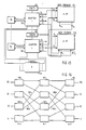
- FIG. 1 of the accompanying drawings is an illustration of one type of computer system being discussed here.
- processors 10 each operating independently and in parallel with each other.
- N the number of parallel processors
- newer designs involve the number N increasing to 256 and perhaps 1,024.
- Each of the processors 10 occasionally requires access to one of several memories 12.
- the memories will be assumed to be equivalent and also of number N.
- Each processor 10 has an input/output (I/O) path 14 and each memory 12 also has an I/O path 16.
- the paths 14 and 16 can be buses and may be duplicated to provide full-duplex communication.
- a processor 10 requiring access to a particular memory 12, requires that its I/O path 14 can be connected to the I/O path 16 of the required memory 12. This selective connection is performed by a switching system 18, which is seen to be central to the design of the distributed processing of the computer system illustrated in Figure 1.
- the cross-point switching system of Georgiou has the further advantage of being non-blocking.
- non-blocking is meant that if a processor 10 requires that its I/O path 14 be connected to the I/O path 16 of a memory 12 not currently connected, the switch 18 can always provide that connection. Thus, a processor 10 is not blocked by the switching system 18 when it requires a connection.
- Georgiou has also described in European Patent Application 141,233A a controller for his cross-point switching system. Georgiou's controller is designed to be very fast but it suffers from the deficiency of most cross-point switching systems that one controller is used for all N input ports. As a result, the controller must sequentially service a plurality ports requesting connection through the cross-point switching system. That is, the controller is a shared resource. Therefore, once the demanded connection rate exceeds the speed of the controller, the throughput of the combined cross-point switching system and the controller falls as N ⁇ 1.
- the port connection table of Georgiou's invention is also a shared resource and limits the controller's speed for large values of N.
- Delta network switching system An alternative to the cross-point switching system is the Delta network switching system.
- Delta network switching systems are defined, with several examples provided, by Dias et al in a technical article entitled “Analysis and Simulation of Buffered Delta Networks” appearing in IEEE Transactions on Computers, Vol. C-30, No. 4, April 1981 at pp. 273-282.
- Patel also defines a Delta network switching system in "Performance of Processor-Memory Interconnections for Multiprocessors", IEEE Transactions on Computers, Vol. C-30, No. 10, October 1981 at pp 771-780.
- a Delta network switching system will be described here by way of example with reference to the Omega switching network, described by Gottlieb et al in a technical article entitled "The NYU Ultracomputer-Designing and MIMD Shared Memory Parallel Computer", appearing in the IEEE Transactions on Computers, Volume C-32, No. 2, February 1983, at pages 175-189.
- This example of a Delta network switching system is illustrated in Figure 2 of the accompanying drawings.
- Connecting the right hand and the left hand ports are three stages of switches 20.
- Each switch 20 is a 2 ⁇ 2 switch that can selectively connect one of the two inputs on one side to one of the two outputs on the other side. It is seen that the illustrated Delta network switching system can provide a connection from any port on the right hand side to any port on the left hand side.
- This Delta network switching system is intended to be used in a parallel pipelined fashion. Data is transmitted from one side to the other in relatively small packets. Each packet contains, in addition to the data, control information, including the address of the desired destination. For instance, if the left-hand port 000 desires to send a packet of data to the right hand port 100, it includes the destination address 100 in the header of the packet and inputs the packet into the switch 20a.
- the switch 20a looks at the right-most bit of the destination address and, as a result, sends both the destination address and the data part of the packet through its 0 output to switch 20b.
- the switch 20b looks at the middle bit of the destination address, a 0, and routes the package likewise through its 0 output to switch 20c.
- the switch 20c looks at the third or left-most bit of the destination address, a 1, and thus routes the packet through its 1 output to the right hand port 100.
- the Delta network switching system of Figure 2 can provide parallel transmission paths, thus increasing the bandwidth of the switching system.
- the Delta network switching system illustrated is a blocking network; that is, there is no guarantee that a connection path is available through the switching system even if the desired output port is otherwise available. For instance, if the previously described connection between the 000 port on the left-hand side and the 100 port on the right-hand side is made, the left-hand port 001 is blocked from reaching the four right-hand ports 000, 010, 100 and 110. The previously described connections would need to be broken before the blocking is removed.
- a Delta network switching system is potentially fast, but, as traffic increases, blocking delays can be expected.
- the object of the present invention is to provide an improved switching system for transmission of data.
- the invention relates to a switching system for transmission of data comprising a non-blocking switching matrix partitioned into a plurality of selectable data transmission paths, these paths providing connections between each of a plurality of first ports of the matrix and selected ones of a plurality of second ports of the matrix, first path control means for controlling each data transmission path for completing each selected connection, and system control means responsive to a message requesting a connection between a first port and a selected second port to establish the requested connection, all first path control means and all system control means operating in parallel.
- the switching system is characterised in that the system control means provides message buffers allowing a pipelined switching of message information and furthermore provides for the establishment of the requested connection beginning at a determined time based upon prior established connections to the selected second port, and the path control means establishes the requested connection at the determined time so as to provide for transmission of data from the first port to the selected second port.
- the switching system includes a cross-point switch which provides high bandwidth, non-blocking connections for data transmission.
- Multiple controllers are provided at either the input or output ports for controlling the cross-point connections to that port.
- An access request to a port is granted on a reservation basis. That is, a control request is made over the Delta network requesting a fixed block of connection time.
- the controller receives these requests and sets up a schedule for connection and perhaps transmits back over the Delta network to the requesting port the time delay before its time connection will be honoured.
- a switching system combines the best features of a cross-point switching system and a Delta network switching system by providing a non-blocking cross-point switch for data transmission and by additionally providing a Delta network switch for switching control information between the input and output ports of the cross-point switching system.
- Parallel controllers for the cross-point switch are provided at each input port of one of the sets of ports of the switching system.
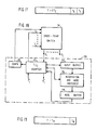
- a cross-point switch 34 has four horizontal lines 36 connected to the input adaptors 30 and four vertical lines 38 connected to the output adaptors 32. At each intersection of a horizontal line 36 and a vertical line 38 is formed a cross-point that is individually selectable to make the connection between the respective horizontal line 36 and vertical line 38.
- a cross-point controller 40 is associated with each horizontal line 36 to control the cross-points of that horizontal line 36. This embodiment thus is horizontally partitioned because the controllers are associated with the input ports rather than the output ports.
- Each cross-point controller 40 is itself controlled by an associated input adaptor 30.
- the cross-point switch 34 is used primarily for the selective transmission of data while a separate Delta network 42 is used primarily for the selective transmission of control information between the input adaptors 30 and the output adaptors 32.
- N 4
- This Delta network differs from that illustrated in Figure 2 in that each switch 44 has its own buffering and the adaptors 30 and 32 also require buffering.
- the Delta network 42 consisting of three stages of four switches 44 in each stage.
- the right-most stage and the left-most stage would each consist of 1 ⁇ 2 switches.
- the buffering for the adaptors 30 and 32 could be performed by the 1 ⁇ 2 switches.
- the fundamental problem in controlling a cross-point switching system is to ascertain whether the desired resources are available, in this case, the required horizontal line 36 and vertical line 38 of the cross-point switch 34.
- Each controller 40 of the horizontally-partitioned cross-point switch is easily able to decide if its associated horizontal line 36 is available.
- a much more difficult problem is for the controller 40 to know if the desired vertical line 38 is available or whether another controller 40 had connected a different cross-point to the desired vertical line 38.
- the Delta network 42 provides the fast and efficient means of obtaining this information.
- an input adaptor 30 When an input adaptor 30 receives a request from its input port I0-I3 for a connection to a designated output port O0-O3, the input adaptor 30 directs this request through the Delta network 42 to the designated output adaptor 32.
- Each output adaptor 32 keeps a record of the use of its associated vertical line 38.
- the request that the input adaptor 30 transmits to the output adaptor 32 is in the form of a control message S C ij where i is the number of the input adaptor 30 and j is the number of the output adaptor 32 that is being requested.
- the first two parameters are the addresses or the numerical designations of the input adaptor 30 and the output adaptor 32 respectively.
- the third parameter T in the message is the length of time that the i-th input adaptor 30 is required to be connected to the j-th output adaptor 32.
- the fourth parameter C is a control field and may contain information such as the requested address to memory and whether the requested connection is for a read or write operation.
- the destination address A j is used for routing the control message S C ij through the Delta network 42 to the designated output adaptor 32.
- the source address A i is used for routing a reply to that request back to the input adaptor 30 through the same
- the address field A contains the destination address A j .
- the switches 44 know on which input port to the respective switch the control message arrived.
- the number of the input port is one bit of the address of the requesting input adaptor 30.
- the switch 44 can replace one of the bits of the destination address A j with the number of the input port used with that switch.
- the address field A contains the source address A i .
- the combined field A provides a shorter control message, thus reducing the probability of a blocked node in the Delta network 42.
- Figure 4 is a time history that shows on the left the time period required for the control message to be transmitted from the input adaptor 30 through the Delta network 42 to the output adaptor 32. This propagation time period may involve delays at one or more switches 44 because the node is blocked.
- Each output adaptor 32 has a time register or reservation clock that shows the time instant t oc at which the output adaptor 32 will have completed processing all connection requests in its reservation queue. This time instant t oc is thus the time at which a new request can be honoured.
- the output adaptor 32 receives the control message S C ij (A,T,C), it replaces the time field T in the control message by the reservation time instant V that is equal to t oc and increments the reservation clock by the time period T.
- the series of operations by the output adaptor 32 can be performed by the fetch-and-add operation described by Gottling.
- the time instant V is never allowed to have a value earlier than the time instant represented by (t+t min ) where t is a time instant from which time periods are measured and t min is the propagation time from the output adaptor 32 back to the input adaptor 30, assuming that there are minimal blocking delays within the Delta network 42 (see Figure 4).
- reservation clock is incremented by t min +T.
- the control message sent back to the input adaptor 30 is S R ij (A,V).
- S R ij A,V
- that adaptor knows the time instant V at which it can initiate the sending of the message to the respective output adaptor.
- the input adaptor 30 instructs its associated controller 40 to make the cross-point switch 34 and the input adaptor 30 then proceeds to send its message.
- the output adaptor 32 has prepared itself to receive the message designated by the senior member of the reservation queue.
- the reservation time instant V may have already passed. If the reservation time instant V received by the input adaptor 30 has passed, as indicated by the system clock, part of the reserved time period at the output adaptor 32 has already expired. Accordingly, it is impossible to transmit the entire desired message and the input adaptor 32 must make another request for the same data message.
- cross-point controllers 40 are associated with the input ports and guarantee against a double use of any horizontal line 36.
- the output adaptors 32 guarantee, by means of the reservation, against a double use of any vertical line 38.
- the description of the above embodiment is adequate for an understanding of the concept of the basic invention. However, it lacks detail as to the hardware necessary for an efficient Delta network. Furthermore, the efficiency of the Delta network can be a greatly increased in heavy traffic situations if control messages can be combined within the Delta Network when two or more input ports are sending control messages to the same output port. There is a high probability at any one time that one of the output ports is receiving a large number of control messages, at a faster rate than it can handle. In such a situation, the node or switch immediately associated with that output port must inhibit all intermediate nodes or switches connected to it from sending further control messages. If the buffering capabilities of the intermediate nodes or switches are exceeded, the inhibition extends through a major part of the Delta network, thus blocking the transmission of control messages to other output ports. Thus, significant buffering should be provided at each of the nodes or switches of the Delta network.
- Figure 5 shows a 16 ⁇ 16 Delta network 50 connected to 16 input adaptors on the left-hand side and 16 output adaptors on the right-hand side.
- the Delta network 50 comprises four stages of nodes or switches 52, each stage identified by a depth from the input adaptors.
- the nodes are all 2 ⁇ 2 switches.
- the outputs of the nodes of depth 3 are connected to respective output adaptors through reservation processors 54, to be described later.
- the nodes 52 are arranged in rows and numbered from 000 to 111 according to the higher order bits of the input lines.
- a particular node can be identified by its row and its depth. For example, node 011(2) is in row 011 at a depth of 2.
- S C ij (A,C,T,D,a,K).
- D, a and K are required for the combining function.
- the first parameter A is the combined address field previously described except for the inclusion of an extra bit. For example, a message from input adaptor 0001 intended for an output adaptor 0001 enters node 000(0) from input adaptor 0001 with an address of x0001.
- the extra left-hand bit is set to 1, i.e., 10001, by node 000(0) to indicate the input port from which it came.
- the second parameter C contains control information, as described previously.
- the control information might include the identifier of a line to be read from storage memory connected to the output adaptor. If the storage has 32 bit addresses (a typical situation in a main frame computer) and 128 byte lines, the storage would require 22 bits of addressing information in the control information C in order to identify the line.
- the control information C would include the type of operation to be performed, e.g., read or write.
- the inclusion of this operational information in the control message allows the accessing delays to the storage to overlap the delays introduced by the cross-point switch and the Delta network 50.
- This control information including an address is particularly useful when data is being accessed from a bulk memory on the destination side that is combined with a cache.
- the addressing information in the control message allows the data to be transferred or pre-fetched from bulk memory to the cache prior to the actual data access through the cross-point switch. For instance the address would be a line address for 128 bytes of data.
- the control information C further contains an indicator as to whether the original control information was left behind in a message combining operation or, alternatively, an identifier of a message which was combined into a combined message that has the highest priority and thus retains the associated addressing information.
- the parameter T is the time period required for the operation if there is no provision for overlapping of accessing delays and switching delays.
- the connection time period T that is originally requested would be a single unit, e.g., the unit of time required to read one line of a memory.
- the parameter T could be increased if messages are combined at the intermediate node.
- the remaining parameters D, a and K, in the forward control message S C ij are required for the combining operations at the nodes.
- the parameter a is an identifier, inserted by a combining node to identify for its own use the combining operation that produced the combined message. The combining nodes associate the identifier a with control messages retained in its own buffer.
- the parameter K is the number of nodes at which combining was done for a given message. When a control message has been combined, a reply message in the opposite direction must be decombined, thus producing a delay in the backward path.
- the parameter K is a measure for the delay for the highest priority message on the return path and serves to determine the earliest reservation time which could be used. Initially, K is set at zero.
- Each node of the Delta network 50 has a structure schematically represented in Figure 6.
- Control data is received in the forward direction on two forward data input paths 60 and 62 from the previous stage of nodes.
- the forward control data is received, controlled, possibly buffered and then switched to one of two forward data output paths 64 and 66. These functions are controlled by a forward direction control and buffering circuit 68 to be described in detail later.
- the forward data output paths are connected to the next stage in the Delta network 50.
- This structure is generally duplicated for control messages sent in the return direction by return data input paths 70 and 72 and return data output paths 74 and 76 connected by a return direction control and buffering circuit 78.
- Each of the data paths 60 to 66 and 70 to 76 has an associated inhibit line going in the reverse direction to or from the same node in the neighbouring stage.
- a control and buffering circuit 68 or 78 Whenever a control and buffering circuit 68 or 78 has filled its output buffers so that no more messages can currently be handled, it puts an active signal on both of its output inhibit lines 80 and 82 or 88 and 90. This inhibition indicates to both of the neighbouring nodes on one side, which are possibly transmitting to that circuit 68 or 78, that no more messages should be transmitted.
- the forward direction control and buffering circuit 68 detects an active signal on inhibit line 84, it will not transmit control messages on the associated data path 64.
- the return direction and control buffering circuit 78 detects an active inhibit signal on line 92, it will not transmit a return control message on the associated data path 74.
- a combined request buffer 96 is accessible by both the forward and reverse direction control and buffering circuits 68 and 78 for the storage and subsequent retrieval of combined messages.
- a fullness register 98 keeps track of the number of messages currently being stored in the combined request buffer 96.
- the fullness register 98 is incremented by the forward direction control and buffering circuit 68 when it stores a message in the combined request buffer 96.
- the return direction control and buffering circuit 78 decrements the fullness register 98 when it retrieves a message from the combined request buffer 96.
- the messages stored in the combined request buffer 96 are indexed by an identifier provided by the forward direction control and buffering circuit 68. There are only a finite number of allowed identifiers and the list register 100 keeps track of which identifiers are in use.
- the list register 100 could be an 8-bit register.
- the forward direction control and buffering circuit 68 would set the bit corresponding to an identifier indicating that it is being used for messages being stored in the combined request buffer 96.
- the return direction control and buffering circuit 78 retrieves the last identified message from the combined request buffer 96, it resets the corresponding bit in the list register 100 to indicate that that identifier is now available.
- the forward direction control and buffering circuit 68 is shown in more detail in Figure 7.
- Input buffers 110 and 112 are connected to the forward data input paths 60 and 62 and are of sufficient size to contain one control message S C ij apiece.
- the input buffers 110 and 112 have a further function of modifying the address in the combined address field A. This can be easily accomplished by tying the output of the address bit to be modified to a zero value for the input buffer 110 and to a one value for the input buffer 112, regardless of the value of that bit input to the input buffer 110 or 112. For instance, in the previously described example, for the 000(1) node the left-most address bit is always output as a 1 from the input buffer 112.
- a path control circuit 114 controls the routing of messages between the input buffers 110 and 112 and the forward data output paths 64 and 66 as well as the routing to and from an output buffer 116 controlled by a buffer and combination controller 118.
- a fullness register 120 which indicates the number of messages stored in the output buffer for transmission on the forward data output paths 64 and 66.
- the path control circuit 114 immediately forwards a message from the input buffer 110 or 112 to its indicated output path 64 or 66 if the output buffer 116 is empty, as indicated by the fullness register 120, and if the path 64 or 66 is available.
- the path 64 or 66 is available if two conditions are satisfied.
- the inhibit line 84 or 86 associated with the data output path 64 or 66 must be off. Futhermore, the message in the input buffer 110 or 112 must be the only message in the input buffers 110 and 112 for the indicated path. That is, the other input buffer must either be empty or contain a message directed to the other output path. If, however, both input buffers 110 and 112 contain messages directed to the same output path 64 to 66, there is a conflict or contention for that output path.
- One method of solving the contention is to proceed with the combining operation to be described later. However, in order to minimise forwarding delays in the light traffic situation when the output buffer is empty, it is recommended that the contention be immediately resolved by the path control circuit 114.
- the path control 114 keeps track of which of the input buffers 110 and 112 has last forwarded a message to the output path 64 or 66.
- the input buffer 110 or 112 which was not the last to forward is given priority in the contention and its message is forwarded before the other. That is, the path control circuit 114 causes priority to alternate between the input buffers 110 and 112.
- the output buffer 116 stores messages waiting to be forwarded on the data output paths 64 and 66.
- the output buffer 116 must be content addressable both for the remaining destination address part of the combined address field A, to be used in the combining process, and for the two addresses of the two data output paths 64 and 66.
- the output buffer 116 must operate as a first-in/first-out buffer for all of its contents addressed respectively to the two data output paths 64 and 66. These functions can be easily performed by dividing the output buffer 116 into two output buffers or sub-buffers 116a and 116b, as shown in Figure 8. Each of the output buffers 116a and 116b is dedicated to respective data output paths 64 and 66.
- Fullness registers 98a and 98b are associated with the respective divided buffers 116a and 116b.
- Associated with each output buffers 116a or 116b is an H register 122a or 122b and a T register 124a or 124b.
- the H and T registers are used for pointers to control the first-in/first-out buffering function.
- the memory organisation of an output buffer 116a or 116b is shown in Figure 9.
- the buffer 116a or 116b consists of n+1 addressable storage locations, each storing one control message S C ij .
- the T register 124a or 124b points to the next storage location in the output buffer 116a or 116b in which a message is to be stored.
- the H register 122a or 122b points to the oldest stored message which will be the next message to be retrieved.
- Figure 9 illustrates three storage locations for three messages currently being stored in the buffer.
- the T register is decremented by 1.
- the H register 122a or 122b is decremented by 1.
- FIG. 10 A more detailed schematic showing the circuitry associated with the path control circuit 114 is illustrated in Figure 10.
- a buffer status register 130 or 132 that contains two bits of information (b1,b2).
- Two additional registers 134 and 136 are associated with each of the data output paths 64 and 66 and indicate the source of the last message transmitted on that line. That is, the contents of the last message register 134 associated with the data output path 64 is set to 0 if the last message transmitted on path 64 was received for data input path 60 and is set to 1 if the message was received on data input path 62.
- the path control circuit 114 increments the fullness register 120a when a message intended to be transmitted on the data output path 64 is buffered in the output buffer 116a. When the buffered message is retrieved from the output buffer 116a and transmitted on the data output path 64, the path control circuit 114 decrements the fullness register 120a. Similar incrementing and decrementing is performed upon the fullness register 120b as messages are buffered in the output buffer 116b for transmission on the data output path 66.
- the fullness register 120a is interrogated through the buffering and combination controller 118 to determine if it contains a non-zero value, that is, that there are messages waiting in the output buffer 116a. If the fullness register 120a is greater than 1, then the next message in the output buffer 116a is retrieved and the fullness register 120a is decremented. The last message register 134 is then updated according to the origin of this message and the message select flag is set.
- a message in the upper input buffer 110 is immediately forwarded to the data output path 64 if either: (1) the content of the last message register 134 is 0 and the contents of the buffer status register 130 are (1,0), or (2) the content of the last message register 134 is a 1, the contents of the upper buffer status register 130 are (1,0) and the first bit b1 of the lower buffer status register 132 is 0.
- a message is transmitted from the lower input buffer 112 if either: (1) the content of the last message register 134 is 1 and the contents of the lower buffer status register 132 are (1,0), or (2) the content of the last message register 134 is 0, the contents of the lower buffer status register 132 are (1,0) and the first bit b1 of the upper buffer status register 130 is 0. If a message is to be sent under any of these conditions, then the message select flag is set. If however, either the upper or lower input buffers 110 or 112 have an incoming message which cannot be immediately forwarded because none of the above conditions are satisfied, then the message is forwarded to the buffer and combination controller 118.
- the operation of the buffer and combination controller 118 will now be described as it buffers and possibly combines a message.
- the controller 118 receives a control message S C (A,C,T,D,a,K) from the path control 114. It is assumed that the node 52 is at a depth of d.
- the controller 118 takes the remaining bits of the combined address field A that designate the destination address, that is, a d+1 , a d+2 ..., and compares them with the corresponding bits of messages already stored in the output buffer 116. That is, the output buffer 116 is content addressable according to the field a d+1 , a d+2 , . . ..
- the output buffer comprises two output buffers 116a and 166b associated with the two data output paths 64 and 66, the first bit a d+1 points to one or the other of these two output buffers 116a and 116b. These two buffers 116a and 116b are then individually content addressable to the remaining address bit or bits a d+2 , a d+3 . . ... However, the two output buffers 116a and 116b are content addressable only between their respective T and H pointers for the valid messages currently stored therein.
- the T register 124a or 124b is decremented and the associated fullness register 120a or 120b is incremented. This completes the buffering operation and no message combining was performed.
- M i (A i ,C i ,T i +T,D i ,a i ,K i ) for the newly combined stored message.
- the incremented time period parameter is the total time period required to service all the tasks of all the combined control messages.
- the last parameter a i has been taken from the already combined message M i and is one of the identifiers used to identify which catalogued message M* are associated with a single combined message M i as well as to identify the message that will eventually be returned from the reservation processors 54.
- the buffer and combination controller 118 increments the associated fullness register 98. Once the control message S C has been combined into the buffered message M i and its associated catalogued message M* has been stored, the buffer and combination controller 118 is ready for the next cycle.
- the identifier a' is a new identifier that is indicated as being currently unused in the list register 100.
- the list register 100 is then changed to indicate that the identifier a' is now in use. If no further identifiers are available, the inhibit lines 80 and 82 are set active to prevent the reception of further messages.
- the buffer and combination controller 118 causes the inhibit lines 80 and 82 to go active to prevent the further reception of messages that could perhaps cause the combined request buffer 96 to overflow.
- the parameters A i , C i and K i for inclusion in the newly combined message M i were arbitrarily selected from the already stored but never combined message M i . These parameters could equally well have been taken from the control message S C . It is possible to set up a priority scheme in the control parameter C such that the message with the highest priority always retains its parameters upon combining. This is particularly useful when the control parameter C is being used as addressing information at the destination port. Of course, only one such set of addressing information can be transmitted in the control field C i in a combined message M i .
- a message in the output buffer 116a or 116b should not be involved in a combining operation if that message is already at the top of the queue.
- An attempt to combine the senior member of the queue is likely to result in a delay in the transmission of messages from the buffer. Accordingly, referring to Figure 9, only those messages located at or between the locations T+1 and H-1 are content addressable for the address bits a d+1 , a d+2 , . . ..
- a list register 100' contains one location for each of the identifiers a.
- a usage bit indicates whether the associated identifier a is currently in use. The identifier itself needs not be stored but can simply be the address of the location.
- a length parameter indicates the number of catalogued messages in a combined request buffer 96' that are catalogued by the identifier a. Finally, for every identifier a, there is a pointer to a location of one of the catalogued messages in the combined request buffer 96'.
- the combined request buffer 96' is another memory having multiple locations.
- An occupancy bit indicates whether a location is at present being used for storage of a catalogued message M*.
- the location further contains a pointer to another location in the combined request buffer 96' for another message associated with the identifier a.
- the combined request buffer 96' can store catalogued messages M* for any combination of identifiers a in any combination of storage locations.
- the combined request buffer 96' is thus addressable by the identifier a which points to one of a series of catalogued messages. Whenever another catalogued message is stored in the combined request buffer 96' the string of pointers is traced to the last catalogued message, M3* in the illustrated example. Then the occupancy bits of other locations are tested to see if those locations are available.
- the new catalogued message is stored in the pointed-location, the occupancy bit is changed to one and the length parameter is the list register 100 is incremented by one. It should be noted that, in this scheme, the second identifier a' in the catalogued message M* is redundant since this information is available from the string of pointers.
- control messages S C can be immediately forwarded from one node to another node at a different depth, or the control messages can be transmitted in uncombined form after temporary storage in the output buffer 116a or 116b, or a combined control message can be transmitted from the output buffer 116a or 116b.
- control messages may be combined at different depths with corresponding catalogued messages M* being left behind at the combined request buffer 96 at the various depths of combining.
- Each control message S C is eventually received at a designated reservation processor 54, illustrated in Figure 12. It is immaterial to the reservation processor 54 if the control message S C is a combined message or an uncombined message. They are both treated the same.
- the received control message S C is stored in an input buffer 130.
- the address field A, the depth parameter D and the identifier a of the control message S C are immediately forwarded to an output buffer 132 for inclusion in the return message S R .
- the control information C is forwarded to the corresponding output adaptor 32.
- the output adaptor 32 has a cache memory and the control information C contains the address for the page of memory required from the bulk memory associated with the output adaptor 32, then the page can be pre-fetched into the cache memory along with its memory address for quick access when the connection through the cross-point switch 34 is finally completed.
- a reservation processor unit 134 receives the time period parameter T and the number of combining levels K from the input buffer 130.
- the time period T is the total time being requested, possibly for a number of combined messages.
- the number of combining levels K is associated with only one of the uncombined messages in the control message S C .
- a switching system clock provides a real time instant signal t to the reservation processor unit 134.
- a register 136 contains the absolute time instant t oc representing the beginning of the first available reservation. This time instant t oc is set by the reservation processor unit 134 but is always equal to or later than the system clock time instant t. This function can be easily implemented by a comparison circuit.
- the purpose of the reservation processor 134 is to calculate an absolute reservation time instant V for transmission back through the Delta network and for calculating new values of the available reservation time instant t oc .
- the parameter t is the system clock time instant and t oc is the current time instant in the register 136.
- the parameter t min is a parameter of the switching system and represents the time period required for the return message S R to traverse the Delta network 42 back to the input adaptor 30. This parameter is for the case where there has been no combining, and hence no decombining is required for the return message.
- the parameter Z is the expected additional decombining delay for decombining at one node 52.
- the available reservation time register 136 is incremented by the wasted time period P and the requested reservation time period T.
- the new value of the available reservation time instant t oc is thus the time instant when the processing of all the tasks associated with the control message S C have been completed.
- the time instant V transmitted in return message S R is set to the current time instant t oc of the available reservation time register 136 and this register is then updated by the reservation time request period T.
- the propagation of the return control message S R through the Delta network 52 is very similar to the propagation of the forward control message S C through this same network.
- the return direction control and buffering circuit 78, illustrated in Figure 13 is very similar to that of the forward direction control and buffering circuit 68 of Figure 7.
- the switching between the return data input paths 70 and 72 and the return data output paths 74 and 76 is performed according to one bit of the combined address field A in the return message S R .
- the bits in the combined address field are read from right to left.
- the return messages are buffered in input buffers 140 and 142.
- a return path control circuit 144 controls the switching of return message S R through the switch.
- An output buffer 146 is similar to the output buffer 116 except that it does not need to be content addressable but operates strictly as a first-in/first-out buffer.
- a fullness register 147 maintains a count of available slots in the output buffer 146.
- the output buffer 146 and the fullness register 147 may be implemented as dual buffers and registers, as shown in Figure. 8.
- the path control circuit 144 receives those messages through a buffer and decombination controller 148 for transmission on the return data output paths 74 and 76 according to the proper bit in the address field A. For every message taken from the output buffer 146, an associated fullness register 147 is decremented. If the fullness register 147 is decremented when the inhibit lines 88 and 90 are active, the inhibition is removed. Just as in the case of the forward switching, the return messages are transmitted only when the required data output path 74 or 76 is available.
- the output buffer 146 is empty, as indicated by its associated fullness register 147, then a message in the input buffer 140 or 142 is transmitted to the proper data output path 74 or 76 if that path is available and if the depth parameter D in the return message S R (A,V,D,a) does not indicate that decombining is required at this depth, that is if D does not equal d. If the return message S R cannot be forwarded immediately, then it is sent to the buffer and decombination controller 148.
- the controller 148 upon receiving a return message from the path control circuit 144, stores that message in the output buffer 146 if D does not equal d. It then also increments the fullness register 148. When the fullness register 148 indicates that the output buffer 146 is full, the inhibit lines 88 and 90 are set active to inhibit the transmission of further return messages.
- the effect is to allocate the reservation time instant V in the combined return message S R to the various decombined messages.
- the fullness register 120 must be properly incremented and the transferring must be stopped when it indicates that the output buffer 116 is full. In this case, the inhibit lines 88 and 90 are activated.
- any combined return messages S R are decombined at the same level and node at which the control message S C producing them had been combined.
- a single return message may be decombined at more than one depth if the depth parameter D in the catalogue message M* indicates the further need of decombining.
- return messages arrive back at the input adaptors 30 as single, uncombined return messages.
- the input adaptor 30 uses the reservation time instant V contained in the returned message S R as the time instant to cause the associated controller 40 to make the required cross-point connection in the cross-point switch 34.
- the controller 40 must disconnect the cross-point because another cross-point controller is likely to make a conflicting connection based on another granted reservation.
- the buffer and combination controller 118 (Fig. 7) checks the fullness registers 120a and 120b (Fig. 8) associated with the two input buffers 116a and 116b to determine that both buffers have at least two slots available.
- the controller 118 also checks the fullness register 98 associated with the combined request buffer 96 to determine if at least four slots are available.
- the buffer and combination controller 118 sets the inhibit lines 80 and 82 if either of the two above conditions is not satisfied or resets them if both conditions are satisfied.
- the set or reset condition then continues for the next cycle, at the end of which the testing is repeated.
- the buffer and decombination controller 148 checks each fullness register associated with each sub-buffer of the output buffer 146, assuming the dual sub-buffer implementation of Figure 8. Each sub-buffer must have at least the number of slots available that is the greater of 2 or the maximum value length parameter in the list register 100' associated with the combined request buffer 96' ( Figures 11 and 13). If these conditions are met, the buffer and decombination controller 148 resets the inhibit lines 88 and 90. Otherwise they are set active for the following period.
- the previous description relies upon the calculation and transmission back to the input adaptor of the absolute reservation time instant V.
- An alternative approach is to calculate at each reservation processor 54 the reservation delay time period before the associated output adaptor 32 becomes available.
- the delay time period must be greater than the expected return delay time period ZK plus possibly an additional delay time period which accounts for typical blockage time periods. This typical blockage delay time period can be tuned for particular systems.
- the new reservation delay time period is used to update a delay clock at the reservation processor which also decrements to a zero value so as to maintain a real-time delay indicator.
- each node decrements this delay according to the time period that it has actually delayed the return message, either for blockage delays, for buffering delays, or for normal forwarding delays.
- this reservation delay time period signal arrives back at the input adaptor 30, it indicates the true time period delay before the controller 40 should make the required cross-point connection.
- Reservation time period delays in combined returned messages are decombined in the same way as were the reservation time instants V i .
- each device D i For full-duplex communication between the two devices D i and D j , it is recommended that each device D i have two input ports I i and I' i to a cross-point switch 150, illustrated in Figure 14 and similarly have two output points O' i and O i from that switch 150.
- a full-duplex path is provided to the device D i by the two ports I i and O' i when the request for connection had been made by that device D i .
- the duplex path to the device D i is provided by the ports I' i and O i .
- a single cross-point controller 40 associated with the input port I i controls the cross-point connections for both the input port I i and the output port O' i .
- the cross-point connections are between I i and O j and between O' i and I' j . It is seen that the horizontal partitioning of the cross-point switch 150 is maintained.
- the cross-point switch 150 required for the system of Figure 14 is somewhat unusual in that some paths are for data transmission in one direction and other paths are for data transmission in the other direction. It may be preferable to divide the cross-point switch 150 into two cross-point switches 152 and 154, shown in Fig. 15. A single set of controllers 40 connected to the adaptors 30 control the cross-point connections on both switches 152 and 154. Each adaptor 30 has a source-side port and a destination-side port connected to the Delta network 42. It should be noted, however, that the cross-point switch 154 is vertically partitioned rather than horizontally partitioned, at least within the meaning of that term for Figure 3, so that horizontally partitioned cross-point arrays have the control lines parallel to the input lines.
- the advantage of the full-duplex design of Figure 15 is that all data flow through the two cross-point switches 152 and 154 is uni-directional, thus allowing a simple design for the switches 152 and 154.
- the circuitry of Figure 15 assumes that the Delta network 42 is two-way, that is return messages S R are sent back to the source device, D i in the example. If the Delta network 42 is one-way so that no return messages are generated and the cross-points are set on the destination side, then the forward cross-point array 152 would be vertically partitioned and the reverse array 154 would be horizontally partitioned, with a corresponding change in the control lines from the controllers 40.
- the switching systems described above have required both a cross-point switch and a separate Delta network. However, it is possible to use a single cross-point switch for both of the switching functions.
- the cross-point switch is time-multiplexed so that for a fixed period it is operating as a cross-point switch; but, in another fixed period, the cross-point switch is simulating a Delta network.
- This combination of functions can be obtained for a type of Delta network known as a perfect shuffle Delta network, an example of which is illustrated in Figure 16.
- a perfect shuffle Delta network an example of which is illustrated in Figure 16.
- the end stages at a depth d of 0 and 2 are composed of 1 ⁇ 2 switching nodes 160 while the middle stage at a depth of 1 is composed of 2 ⁇ 2 switching nodes 162.
- Perfect shuffle networks are described in the previously cited technical article by Dias et al. Perfect shuffle networks and their use are further described by Stone in a technical article entitled "Parallel Processing with the Perfect Shuffle” appearing in IEEE Transactions on Computers, Vol. C-20, No. 2, February 1971 at pp. 153-161.
- a cross-point switch can simulate a perfect shuffle network because an adaptor connected to both an input port and an output port from the cross-point switch can act as one of the nodes of the perfect shuffle network.
- the adaptor is acting as the corresponding nodes for all the depths of the perfect shuffle network.
- the switching is performed the same regardless of the simulated depth.
- the cross-point switch is multiplexed with a period of T as illustrated in Figure 17.
- T-2T C data is transmitted through the cross-point switch for a period of (T-2T C ).
- T C the time period of the input and output lines.
- the determination of the connection is made by the transmission of the control messages S C .
- the multiplexing period is further divided into two segments, each of length T C . In each of these T C segments, forward control messages S C are transmitted from one adaptor to another, simulating the perfect shuffle network.
- the cross-point connections or switching directions for each of the two T C periods are respectively the two connections dictated by the perfect shuffle network. These connections will not vary depending upon the depth, but will vary for which of the four nodes arranged vertically in Figure 16 is being simulated by the particular adaptor.
- FIG. 18 An apparatus for the multiplexed embodiment of a switching system in accordance with the invention is shown in Figure 18.
- the cross-point switch 34 can be of the same form as that of Figure 3.
- a node circuit 170 that includes the previously described cross-point controller 40 and an I/O adaptor 172.
- the I/O adaptor 172 acts as the input and output adaptors 30 and 32 of Figure 3.
- the I/O adaptor 172 simply connects the input and output ports I" i and O" i from the attached devices to the corresponding input and output ports I i and O i to the cross-point switch 34.
- the controller 40 is making the cross-point connection required for the data transmission.
- the I/O adaptor 172 is possibly receiving control messages S C from the output port O i and immediately forwards them to an input buffer 174. If only one control message is transmitted in each of the segments T C , then the buffer 174 has a capacity of two messages.
- the control messages in the input buffer 174 are sequentially serviced by a reservation and node processor 176.
- the control message must contain two additional parameters, one indicating the depth of the node at which the control message is being received.
- the control message must also contain an indicator as to whether it is a forward control message S C or a return message S R . If the depth parameter indicates that the received control message is intended for a depth of 2, that is the right hand side of the perfect shuffle network of Figure 16, then the reservation and node processor 176 performs similar functions to the reservation processor 54 of Figure 12. Additionally, the reservation and node processor 176, in this case, must change the depth and direction parameters in the control message period.
- the reservation and node processor 176 does not perform the reservation functions upon the message. Instead, the processor 176 associates with the control message a switching direction dependent upon the intended depth parameter and the address field in the control message.
- This switching indicator corresponds to one of the two control segments T C which in turn correspond to the two possible paths from the simulated node.
- the paths 164a and 164b represent one choice and the paths 166a and 166b represent the other choice.
- This switching indicator is also inserted when a control message S C is converted to a return message S R , as described above for the reservation process.
- the node buffer 178 is content addressable according to the switching indicator and operates as a first-in/first-out buffer on those messages.
- the senior message in the node buffer 178 directed in one switching direction is taken from the node buffer 178 and sent to the input port I i .
- the senior member in the node buffer 178 directed to the other switching direction is taken from the node buffer 178 and supplied to the input port I i .
- the cross-point controller 30 is making the connections in the cross-point switch 34 corresponding to the two interconnections illustrated for that node in Figure 16, for example, 164a or 164b and 166a or 166b.
- control messages are being simultaneously received and transmitted by the node circuit 170 in each of the control segments T C .
- the node circuit 170 is also acting as the entry node, additional messages are transmitted between the device attached to the input and output ports I" i and O" i and the reservation and node processor 176.
- a new request for a connection received at the input port I" i is immediately processed by the reservation and node processor 176 to put it in proper form for transmission to the next simulated node.
- the reservation and node processor 176 detects that a return message S R has been received at its final destination, that information is given immediately to the I/O adaptor 172 for use in a subsequent data transmission segment.
- cross-point switch 34 could be used for the immediate transmission of the control message across the entire network, there is no guarantee that two such messages would be simultaneously broadcast to the same destination. This situation is not possible for the time multiplexing of the two control segments T C of the described method.
- the structure of the Delta control network can be advantageously combined with another time multiplexing system to produce a hierarchical control path.
- An example of circuitry usable with the hierarchical system is the switching system of Figure. 15.
- the time sequence is simply shown in Figure 19.
- T-T H the cross-point switch is used for data transmission.
- T H the data transmission is stopped.
- Any adaptor which at that time desires an additional reservation for a connection, transmits similar connection requests S C over both the Delta network and also over the cross-point switch. That is, each adaptor ignores possible contention from other adaptors and causes its controller to make the cross-point connection for the control message S C . It makes the reservation and then returns the confirmation message S R over the cross-point array to the requesting adaptor.
- the destination adaptor receiving a control message over the Delta network, compares the identifier with identifiers received over a time period representing the maximum delay in the Delta network. Once a source adaptor has transmitted a request over the cross-point array, it continues to transmit some signal for the duration of the time period T H . This continued broadcasting prevents the successful receipt of two control messages in the same period T H .
- This hierarchical process allows for very quick connections to be made over the cross-point array in light traffic situations but ensures that the control message is eventually received over the Delta networking regardless of traffic conditions.
Landscapes
- Engineering & Computer Science (AREA)
- Computer Networks & Wireless Communication (AREA)
- Data Exchanges In Wide-Area Networks (AREA)
- Exchange Systems With Centralized Control (AREA)
- Use Of Switch Circuits For Exchanges And Methods Of Control Of Multiplex Exchanges (AREA)
- Multi Processors (AREA)
Claims (12)
- Vermittlungssystem zum Übertragen von Daten, das aufweist:
eine nicht-blockierende Schaltmatrix (34), die in eine Mehrzahl trennbarer Datenübertragungspfade aufgeteilt ist, wobei die Pfade Verbindungen zwischen jedem einer Mehrzahl erster Anschlüsse (o) der Matrix und ausgewählten einer Mehrzahl zweiter Anschlüsse (32) der Matrix liefern,
ein erstes Pfadsteuermittel (30, 40) zum Steuern jedes Datenübertragungspfades, um jede ausgewählte Verbindung herzustellen und
ein Systemsteuermittel (32, 34), das auf eine Nachricht anspricht, die eine Verbindung zwischen einem ersten Anschluß (30) und einem ausgewählten zweiten Anschluß (32) fordert, um die geforderte Verbindung herzustellen, wobei jedes erste Pfadsteuermittel (30, 40) und jedes Systemsteuermittel (32, 42) parallel arbeiten,
dadurch gekennzeichnet, daß das Systemsteuermittel (32, 42) Nachrichtenpuffer (68, 78) bereitstellt, die ein Fließband-Schalten von Nachrichteninformationen ermöglichen und ferner für die Herstellung des geforderten Verbindungsbeginns zu einer bestimmten Zeit sorgt, die auf vorher hergestellten Verbindungen mit dem ausgewählten zweiten Anschluß beruht und das Pfadsteuermittel (40) die geforderte Verbindung zu der bestimmten Zeit herstellt, um für eine Übertragung von Daten aus dem ersten Anschluß zu dem ausgewählten zweiten Anschluß zu sorgen. - Vermittlungssystem nach Anspruch 1, dadurch gekennzeichnet, daß die Schaltmatrix ein Koppelpunktschaltsystem (34) aufweist und das Systemsteuermittel Schaltmittel (42) und ein zweites, jedem zweiten Anschluß (32) zugeordnetes Pfadsteuermittel (32) aufweist.
- Vermittlungssystem nach Anspruch 2, dadurch gekennzeichnet, daß das Schaltmittel (42) ein Deltanetzwerk aufweist.
- Vermittlungssystem nach Anspruch 2 oder Anspruch 3, dadurch gekennzeichnet, daß das Systemsteuermittel folgendes aufweist: ein Übertragungsmittel, um eine Forderungsnachricht für eine Verbindung zu dem zweiten Pfadsteuermittel (32) durch das Schaltmittel zu übertragen und Mittel zum Fließbandverfahren für eine Mehrzahl solcher Forderungsnachrichten für eine Verbindung durch das Schaltmittel.
- Vermittlungssystem nach irgendeinem der Ansprüche 2, 3 oder 4, dadurch gekennzeichnet, daß das Schaltmittel (42) eine Mehrzahl von Stufen aufweist, wobei jede eine Mehrzahl von Schaltknotenmitteln aufweist und die Schaltknotenmittel einer Stufe selektiv mit einem einer Mehrzahl von Schaltknotenmitteln einer anderen Stufe entsprechend Adressierungsinformationen in der Forderungsnachricht für eine Verbindung verbunden sind.
- Vermittlungssystem nach Anspruch 4 oder Anspruch 5, dadurch gekennzeichnet, daß das Übertragungsmittel auch die Forderungsnachricht für eine Verbindung über das Koppelpunktschaltsystem (34) überträgt und die Forderungsnachricht für eine Verbindung eine Forderungsidentifizierung enthält und daß das Systemsteuermittel (32, 42) Mittel aufweist, um Forderungsidentifizierungen von Forderungsnachrichten für eine Verbindung zu vergleichen, die über das Schaltmittel (42) mit Forderungsidentifizierungen von Forderungsnachrichten für eine Verbindung empfangen werden, die über den Koppelpunktschalter (34) erfolgreich empfangen werden.
- Vermittlungssystem nach Anspruch 4, dadurch gekennzeichnet, daß das zweite Pfadsteuermittel (32) die Forderungsnachricht für eine Verbindung empfängt und eine resultierende Antwortnachricht zu dem ersten Pfadsteuermittel überträgt.
- Vermittlungssystem nach Anspruch 6, dadurch gekennzeichnet, daß die Antwortnachricht über das Schaltmittel übertragen wird.
- Vermittlungssystem nach Anspruch 7 oder Anspruch 8, dadurch gekennzeichnet, daß das Schaltmittel (42) eine Mehrzahl von Stufen aufweist, wobei jede eine Mehrzahl von Schaltknotenmitteln aufweist, die Schaltknotenmittel für eine Stufe selektiv mit einem einer Mehrzahl von Schaltknotenmitteln einer anderen Stufe entsprechend Adressierungsinformationen in der Forderungsnachricht für eine Verbindung verbunden ist, wenn die Forderungsnachricht zwischen den verbundenen Knotenmitteln und entsprechend Adressierungsinformationen in der Antwortnachricht übertragen wird, wenn die Antwortnachricht zwischen den verbundenen Knotenmitteln übertragen wird.
- Vermittlungssystem nach Anspruch 9, dadurch gekennzeichnet, daß jedes Schaltknotenmittel Forderungsnachrichten empfängt und folgendes aufweist: Mittel zum Kombinieren einer Mehrzahl empfangener Forderungsnachrichten für eine Verbindung in eine einzelne kombinierte Forderungsnachricht für eine Verbindung zum Übertragen und Mittel zum Zerlegen einer Antwortnachricht, die sich aus der kombinierten Forderungsnachricht für eine Verbindung ergibt, in eine Mehrzahl von Antwortnachrichten zum Übertragen.
- Vermittlungssystem nach Anspruch 10, dadurch gekennzeichnet, daß die Kombinationsmittel und die Zerlegungsmittel einen Nachrichtenpuffer (68, 78) aufweisen, um zumindest einen Teil empfangener Forderungsnachrichten für eine Verbindung zu speichern, die kombiniert sind, und daß die einzelne kombinierte Forderungsnachricht für eine Verbindung nur einen Teil der empfangenen Forderungsnachrichten für eine Verbindung enthält, die kombiniert sind.
- Vermittlungssystem nach Anspruch 4, dadurch gekennzeichnet, daß der Koppelpunktschalter (34) und das Schaltmittel (42) zusammen folgendes aufweisen: einen Koppelpunktschalter, Mittel zum Multiplexen des gemeinsamen Koppelpunktschalters zwischen Übertragung von Daten und Übertragung von Forderungsnachrichten und Mittel an den Anschlüssen des Koppelpunktschalters zum Simulieren des Schaltmittels (42).
Applications Claiming Priority (2)
| Application Number | Priority Date | Filing Date | Title |
|---|---|---|---|
| US71311785A | 1985-03-18 | 1985-03-18 | |
| US713117 | 1985-03-18 |
Publications (3)
| Publication Number | Publication Date |
|---|---|
| EP0195589A2 EP0195589A2 (de) | 1986-09-24 |
| EP0195589A3 EP0195589A3 (en) | 1989-07-19 |
| EP0195589B1 true EP0195589B1 (de) | 1992-06-10 |
Family
ID=24864807
Family Applications (1)
| Application Number | Title | Priority Date | Filing Date |
|---|---|---|---|
| EP86301778A Expired EP0195589B1 (de) | 1985-03-18 | 1986-03-12 | Vermittlungssystem für Datenübertragung |
Country Status (5)
| Country | Link |
|---|---|
| US (1) | US4814762A (de) |
| EP (1) | EP0195589B1 (de) |
| JP (1) | JPS61214694A (de) |
| CA (1) | CA1263729A (de) |
| DE (1) | DE3685599T2 (de) |
Families Citing this family (31)
| Publication number | Priority date | Publication date | Assignee | Title |
|---|---|---|---|---|
| US4897641A (en) * | 1986-12-04 | 1990-01-30 | Pascom Pty. Ltd. | Space switch |
| FR2620285B1 (fr) * | 1987-09-07 | 1990-01-19 | Velikanov Cyrille | Procede et dispositif de commandes de commutations dans un ensemble d'interconnexions |
| US4833468A (en) * | 1987-10-14 | 1989-05-23 | Unisys Corporation | Layered network |
| US4929939A (en) * | 1988-10-31 | 1990-05-29 | International Business Machines Corporation | High-speed switching system with flexible protocol capability |
| US5163149A (en) * | 1988-11-02 | 1992-11-10 | International Business Machines Corporation | Combining switch for reducing accesses to memory and for synchronizing parallel processes |
| US5039986A (en) * | 1988-11-15 | 1991-08-13 | International Business Machines Corporation | High speed dynamic allocator for various length time slots |
| US4952930A (en) * | 1988-11-18 | 1990-08-28 | International Business Machines Corp. | Multipath hierarchical network |
| US4984237A (en) * | 1989-06-29 | 1991-01-08 | International Business Machines Corporation | Multistage network with distributed pipelined control |
| JP2577133B2 (ja) * | 1989-11-27 | 1997-01-29 | スティフティング フォール ド テフニスヘ ウェッテンスハッペン | 船舶のプロペラ |
| KR940002905B1 (en) * | 1989-12-15 | 1994-04-07 | Ibm | Apparatus for conditioning priority arbitration in buffered direct memory addressing |
| JP2770936B2 (ja) * | 1990-12-18 | 1998-07-02 | インターナショナル・ビジネス・マシーンズ・コーポレイション | 通信ネットワークおよび通信チャンネルをつくる方法 |
| EP0600997A1 (de) * | 1991-08-05 | 1994-06-15 | Honeywell Inc. | Nachrichtenformat für anpassungsfähiges selbstweglenkendes blockierungsfreies nachrichtenvermittlungs- und weglenkendes system |
| WO1993003580A1 (en) * | 1991-08-05 | 1993-02-18 | Honeywell Inc. | Scalable self-routing nonblocking message switching and routing network |
| EP0598027A1 (de) * | 1991-08-05 | 1994-05-25 | Honeywell Inc. | Kreuzvermittlungsschalter mit rückkopplungsnetz für anpassungsfähiges selbstlenkendes blockierungsfreies nachrichtenvermittlungs - und lenkendes system |
| EP0602916A3 (en) * | 1992-12-14 | 1994-08-10 | Hewlett Packard Co | Cross-bar interconnect apparatus. |
| JP3483284B2 (ja) * | 1993-12-28 | 2004-01-06 | 富士通株式会社 | 並列プロセッサシステム用ネットワークサブ装置および並列プロセッサシステム用ネットワーク装置 |
| KR0132944B1 (ko) * | 1994-12-23 | 1998-04-21 | 양승택 | 데이터 교환장치 |
| US5742597A (en) * | 1996-03-14 | 1998-04-21 | Motorola, Inc. | Method and device for multipoint switching and arbitration in output-request packet switch |
| US5790545A (en) * | 1996-03-14 | 1998-08-04 | Motorola Inc. | Efficient output-request packet switch and method |
| US5689644A (en) * | 1996-03-25 | 1997-11-18 | I-Cube, Inc. | Network switch with arbitration sytem |
| US5784003A (en) * | 1996-03-25 | 1998-07-21 | I-Cube, Inc. | Network switch with broadcast support |
| US5754791A (en) * | 1996-03-25 | 1998-05-19 | I-Cube, Inc. | Hierarchical address translation system for a network switch |
| DE69833122T2 (de) * | 1997-10-21 | 2006-08-24 | Koninklijke Philips Electronics N.V. | Signalverarbeitungsvorrichtung und verfahren zur verbindungsplanung zwischen prozessoren in einer signalverarbeitungsvorrichtung |
| US6243770B1 (en) * | 1998-07-21 | 2001-06-05 | Micron Technology, Inc. | Method for determining status of multiple interlocking FIFO buffer structures based on the position of at least one pointer of each of the multiple FIFO buffers |
| WO2001026345A1 (fr) * | 1999-09-30 | 2001-04-12 | Fujitsu Limited | Procede et dispositif de commande de creation d'un reseau |
| US6529983B1 (en) | 1999-11-03 | 2003-03-04 | Cisco Technology, Inc. | Group and virtual locking mechanism for inter processor synchronization |
| US6892237B1 (en) | 2000-03-28 | 2005-05-10 | Cisco Technology, Inc. | Method and apparatus for high-speed parsing of network messages |
| US6505269B1 (en) | 2000-05-16 | 2003-01-07 | Cisco Technology, Inc. | Dynamic addressing mapping to eliminate memory resource contention in a symmetric multiprocessor system |
| DE602004001583T2 (de) * | 2003-03-24 | 2007-07-19 | Sony Computer Entertainment Inc. | Crossbar-vermittlungsstelle, zugehöriges betriebssteuerungverfahren und -programm |
| US20060155563A1 (en) * | 2005-01-12 | 2006-07-13 | Banerjee Dwip N | Method, system and article for advance lease negotiation in DHCP |
| TWI453605B (zh) * | 2012-11-13 | 2014-09-21 | Askey Computer Corp | 資料傳輸選擇電路及方法 |
Family Cites Families (9)
| Publication number | Priority date | Publication date | Assignee | Title |
|---|---|---|---|---|
| FR2155120A5 (de) * | 1971-10-08 | 1973-05-18 | Labo Cent Telecommunicat | |
| US4074233A (en) * | 1976-06-30 | 1978-02-14 | Norlin Music, Inc. | Selection switch memory circuit |
| JPS5346216A (en) * | 1976-10-08 | 1978-04-25 | Nec Corp | Time sharing multiplex commnicating unit |
| JPS582513B2 (ja) * | 1978-03-03 | 1983-01-17 | 株式会社日立製作所 | ネットワ−ク駆動方式 |
| JPS55143652A (en) * | 1979-04-25 | 1980-11-10 | Hitachi Ltd | Series-parallel signal converter |
| JPS56119596A (en) * | 1980-02-26 | 1981-09-19 | Nec Corp | Control signal generator |
| US4393381A (en) * | 1981-01-02 | 1983-07-12 | T-Bar Incorporated | Transfer bus matrix |
| DE3369449D1 (en) * | 1982-05-07 | 1987-02-26 | Philips Electronic Associated | Data entry keyboard apparatus |
| US4518960A (en) * | 1982-11-23 | 1985-05-21 | Burroughs Corporation | Speed independent selector switch employing M-out-of-N codes |
-
1985
- 1985-12-18 JP JP60283194A patent/JPS61214694A/ja active Granted
-
1986
- 1986-02-12 CA CA000501736A patent/CA1263729A/en not_active Expired
- 1986-03-12 DE DE8686301778T patent/DE3685599T2/de not_active Expired - Fee Related
- 1986-03-12 EP EP86301778A patent/EP0195589B1/de not_active Expired
-
1987
- 1987-11-25 US US07/125,088 patent/US4814762A/en not_active Expired - Fee Related
Also Published As
| Publication number | Publication date |
|---|---|
| EP0195589A2 (de) | 1986-09-24 |
| CA1263729A (en) | 1989-12-05 |
| DE3685599D1 (de) | 1992-07-16 |
| DE3685599T2 (de) | 1993-01-21 |
| JPS61214694A (ja) | 1986-09-24 |
| EP0195589A3 (en) | 1989-07-19 |
| US4814762A (en) | 1989-03-21 |
| JPH0453358B2 (de) | 1992-08-26 |
Similar Documents
| Publication | Publication Date | Title |
|---|---|---|
| EP0195589B1 (de) | Vermittlungssystem für Datenübertragung | |
| USRE34528E (en) | Delta network of a cross-point switch | |
| US4630258A (en) | Packet switched multiport memory NXM switch node and processing method | |
| US5291482A (en) | High bandwidth packet switch | |
| US5535197A (en) | Shared buffer switching module | |
| US5038343A (en) | High speed digital packet switching system | |
| EP0299473B1 (de) | Vermittlungssystem und Verfahren zur Konstruktion davon | |
| EP0365864B1 (de) | Hochgeschwindigkeitspaketvermittlungsknotenentwurf | |
| US4849968A (en) | Buffer management system | |
| KR100334922B1 (ko) | 효율적인출력요구패킷스위치와방법 | |
| US5224093A (en) | High-speed multi-port fifo buffer circuit | |
| CA1274304A (en) | Crosspoint circuitry for data packet space division switches | |
| JPH01123548A (ja) | 通信交換装置 | |
| PL135975B1 (en) | Distributed control digital switching system | |
| EP0492026B1 (de) | Modulare Pufferspeicherung für ein paketvermitteltes Netzwerk | |
| JPH10107803A (ja) | トラヒックシェーピング装置 | |
| JPH05241947A (ja) | 分散クロスバー・スイッチ・アーキテクチャにおける交換接続の配列。 | |
| US5228032A (en) | Interconnection element for an asynschronous time-division multiplex transmission system | |
| US7142515B2 (en) | Expandable self-route multi-memory packet switch with a configurable multicast mechanism | |
| JPS6298842A (ja) | パケツト交換システム | |
| US7130302B2 (en) | Self-route expandable multi-memory packet switch | |
| JP2583679B2 (ja) | セル交換装置 | |
| EP0369116A2 (de) | TDM-Schaltmatrixsteuerung | |
| JPH01500634A (ja) | 自己ルーチング交換システム |
Legal Events
| Date | Code | Title | Description |
|---|---|---|---|
| PUAI | Public reference made under article 153(3) epc to a published international application that has entered the european phase |
Free format text: ORIGINAL CODE: 0009012 |
|
| AK | Designated contracting states |
Kind code of ref document: A2 Designated state(s): DE FR GB IT |
|
| 17P | Request for examination filed |
Effective date: 19870116 |
|
| PUAL | Search report despatched |
Free format text: ORIGINAL CODE: 0009013 |
|
| AK | Designated contracting states |
Kind code of ref document: A3 Designated state(s): DE FR GB IT |
|
| 17Q | First examination report despatched |
Effective date: 19910527 |
|
| GRAA | (expected) grant |
Free format text: ORIGINAL CODE: 0009210 |
|
| AK | Designated contracting states |
Kind code of ref document: B1 Designated state(s): DE FR GB IT |
|
| PG25 | Lapsed in a contracting state [announced via postgrant information from national office to epo] |
Ref country code: IT Free format text: LAPSE BECAUSE OF FAILURE TO SUBMIT A TRANSLATION OF THE DESCRIPTION OR TO PAY THE FEE WITHIN THE PRE;WARNING: LAPSES OF ITALIAN PATENTS WITH EFFECTIVE DATE BEFORE 2007 MAY HAVE OCCURRED AT ANY TIME BEFORE 2007. THE CORRECT EFFECTIVE DATE MAY BE DIFFERENT FROM THE ONE RECORDED.SCRIBED TIME-LIMIT Effective date: 19920610 |
|
| REF | Corresponds to: |
Ref document number: 3685599 Country of ref document: DE Date of ref document: 19920716 |
|
| ET | Fr: translation filed | ||
| PLBE | No opposition filed within time limit |
Free format text: ORIGINAL CODE: 0009261 |
|
| STAA | Information on the status of an ep patent application or granted ep patent |
Free format text: STATUS: NO OPPOSITION FILED WITHIN TIME LIMIT |
|
| 26N | No opposition filed | ||
| PGFP | Annual fee paid to national office [announced via postgrant information from national office to epo] |
Ref country code: FR Payment date: 19950228 Year of fee payment: 10 |
|
| PGFP | Annual fee paid to national office [announced via postgrant information from national office to epo] |
Ref country code: DE Payment date: 19950330 Year of fee payment: 10 |
|
| PG25 | Lapsed in a contracting state [announced via postgrant information from national office to epo] |
Ref country code: FR Effective date: 19961129 |
|
| PG25 | Lapsed in a contracting state [announced via postgrant information from national office to epo] |
Ref country code: DE Effective date: 19961203 |
|
| REG | Reference to a national code |
Ref country code: FR Ref legal event code: ST |
|
| PGFP | Annual fee paid to national office [announced via postgrant information from national office to epo] |
Ref country code: GB Payment date: 20000420 Year of fee payment: 15 |
|
| PG25 | Lapsed in a contracting state [announced via postgrant information from national office to epo] |
Ref country code: GB Free format text: LAPSE BECAUSE OF NON-PAYMENT OF DUE FEES Effective date: 20010312 |
|
| GBPC | Gb: european patent ceased through non-payment of renewal fee |
Effective date: 20010312 |