EP0195445A2 - Halbleiterspeichergerät mit einer Korrekturfunktion - Google Patents
Halbleiterspeichergerät mit einer Korrekturfunktion Download PDFInfo
- Publication number
- EP0195445A2 EP0195445A2 EP86103788A EP86103788A EP0195445A2 EP 0195445 A2 EP0195445 A2 EP 0195445A2 EP 86103788 A EP86103788 A EP 86103788A EP 86103788 A EP86103788 A EP 86103788A EP 0195445 A2 EP0195445 A2 EP 0195445A2
- Authority
- EP
- European Patent Office
- Prior art keywords
- data
- memory cell
- data read
- correction
- error
- Prior art date
- Legal status (The legal status is an assumption and is not a legal conclusion. Google has not performed a legal analysis and makes no representation as to the accuracy of the status listed.)
- Granted
Links
Images


Classifications
-
- G—PHYSICS
- G06—COMPUTING OR CALCULATING; COUNTING
- G06F—ELECTRIC DIGITAL DATA PROCESSING
- G06F11/00—Error detection; Error correction; Monitoring
- G06F11/07—Responding to the occurrence of a fault, e.g. fault tolerance
- G06F11/08—Error detection or correction by redundancy in data representation, e.g. by using checking codes
- G06F11/10—Adding special bits or symbols to the coded information, e.g. parity check, casting out 9's or 11's
- G06F11/1008—Adding special bits or symbols to the coded information, e.g. parity check, casting out 9's or 11's in individual solid state devices
-
- G—PHYSICS
- G06—COMPUTING OR CALCULATING; COUNTING
- G06F—ELECTRIC DIGITAL DATA PROCESSING
- G06F11/00—Error detection; Error correction; Monitoring
- G06F11/07—Responding to the occurrence of a fault, e.g. fault tolerance
- G06F11/08—Error detection or correction by redundancy in data representation, e.g. by using checking codes
- G06F11/10—Adding special bits or symbols to the coded information, e.g. parity check, casting out 9's or 11's
- G06F11/1076—Parity data used in redundant arrays of independent storages, e.g. in RAID systems
Definitions
- the present invention relates to a semiconductor memory device wherein a data storage circuit including a memory cell and an error correction circuit for correcting error data caused by soft errors are formed on a single semiconductor chip and, more particularly, to a semiconductor memory device with an error correction function used in a computer which can reliably prevent storage of data errors.
- each device comprises one or more redundant-bit memory cells in addition to a given number of memory cells.
- error correction data calculated by a given rule is written in advance not only in a memory cell group for storing normal data but also in the redundant-bit memory cell.
- storage data in the memory cell group corresponding to an input address and in the redundant-bit memory cell arranged corresponding thereto are read out therefrom and checked. If no error occurs in the storage data in the memory cell group, the data is output without being modified, and if an error occurs, the data is corrected and then output.
- Such a conventional semiconductor memory device has the following drawbacks.
- a second drawback of the conventional memory device is prolonged data write/read period.
- data write mode data is written in normal data storage memory cells, and at the same time, error correction data calculated by a correction circuit must be written in the redundant-bit memory cell in the identical word block.
- data read mode data respectively read out from the memory cell group and the redundant-bit memory cell are checked by a decoder. If error data is found, it must be corrected by the correction circuit.
- extra time in the data read/write modes prevents realization of high-speed computers.
- the present invention has been made in consideration of the above situation, and has as its object to provide a semiconductor memory device with an error correction function, which can prevent accumulation of storage data errors due to soft errors, and has a short data-read access time like a normal storage device with no error correction function.
- a semiconductor memory device comprising: a memory cell array; data read/write means for reading out storage data from the memory cell array in data read, write and refresh modes, and for rewriting data thereafter; data output means for outputting, to an external circuit, data which is read out from the data read/write means and not subjected to error detection/ correction; and error detection/correction means for causing the readout data from the data read/write means to be subjected to error detection/correction and for supplying the error-corrected data to the data read/write means as rewritten data in the data read and refresh modes.
- a semiconductor memory device comprising: a memory cell array consisting of a plurality of memory cells arranged in a matrix in X and Y directions; internal address generating means for generating a Y direction address based on an X direction address for selecting the memory cell array in a refresh mode; data read/write means for reading out storage data from a given memory cell in the memory cell array which is designated by a pair of X and Y direction addresses, and for rewritten data; and error detection/correction means for causing the readout data from the data read/write means to be subjected to error detection/ correction, and for supplying the error-corrected data to the data read/write means as rewritten data.
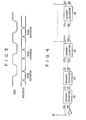
- Fig. 1 is a block diagram showing an overall arrangement when the present invention is applied to a dynamic RAM.
- reference numerals 11A and 11B denote memory cell arrays, each consisting of a plurality of memory cells arranged in matrix in row and column directions.
- Reference numerals 12A and 12B are row decoders for selecting a column of memory cells from memory cell arrays 11A and 11B in response to n-bit row addresses RA1 to RAn input from an external circuit.
- Reference numeral 13 denotes a column decoder/sense amplifier which selects one or more memory cells from a column selected by row decoder 12A or 12B in response to n-bit column addresses OCA1 to OCAn input from an external circuit or (n-m)-bit internal column addresses ICA1 to ICA(n-m), and performs the data read/write operation with respect to the selected memory cells.
- Reference numeral 14 denotes an output buffer which externally outputs, as data Dout, 1 bit of data read out from memory cell arrays 11A and 11B by amplifier 13 in the data read mode.
- Reference numeral 15 denotes a reference clock generator for generating reference clock signal ⁇ based on row-address strobe signal RAS and column address strobe signal CAS.
- Reference numeral 16 denotes a counter circuit which counts reference clock signal ⁇ generated from generator 15 to produce (n-m)-bit internal column addresses ICAl to ICA(n-m).
- Reference numeral 17 denotes an input buffer to which input data Din to be written is supplied.
- Reference numeral 18 denotes an encoder circuit to which output data from input buffer 17 and upper bits OCA(n-m+l) to OCAn of n-bit column addresses OCA1 to OCAn are supplied in the data write mode.
- Reference numeral 19 denotes a decoding/correction circuit which performs decoding processing based on data read out by amplifier 13, and corrects the readout data if an error is detected therein.
- Circuits 18 and 19 are connected to amplifier 13 through (2 m + l ) pairs of data input/output lines i/o and i/o . Note that circuit 18, for example, calculates data in check bit to determine whether the odd or even number of data is at HIGH level. Circuit 19 also performs data encoding and correction like circuit 18.
- Amplifier 13 and circuits 18 receive write enable signal WE. Circuit 18 is activated when signal WE is at LOW level.
- Fig. 2 is a detailed circuit diagram of memory cell arrays 11A and 11B together with row decoders 12A and 128, and column decoder/sense amplifier 13.
- addresses are multiplexed, and row and column addresses are supplied through an identical input terminal. For this reason, the bit numbers of the row and column address must inevitably be the same.
- the row and column addresses have an n-bit configuration, 2 n x 2 n memory cells for storing normal data are arranged in the row and column directions. Therefore, memory cells 21 for storing normal data indicated by squares in Fig. 2 are arranged in a 2 n x 2 n matrix in the row and column directions.
- 2 2n memory cells 21 as a whole are provided in memory cell arrays 11A and 11B.
- Memory cells 21 of each column are commonly connected to one of 2 n word lines WL.
- memory cells 22 for storing the check bit are provided to each 2 m memory cells 21 connected to given word line WL.
- 2 m memory cells 21 and l memory cells 22 constitute each word block 23. Therefore, the total number of memory cells in memory cell arrays 11A and 11B is 2 2n + 2 2n-m x l.
- circuit 19 performs error correction processing. Error-corrected data is again input to amplifier 13 through lines i/o and i/o , and is written in respective cells in original block 23.
- Amplifier 13 is connected to a pair of data input/output lines I/0 and I/O used in a normal data read mode, in addition to lines i/o and i/o .
- strobe signal CAS is set at LOW level
- column addresses OCA1 to DCAn are input to a chip in sync therewith.
- a plurality of word blocks 23 on given word line WL in memory cell arrays 11A and 11B (which is selected by row decoders 12A and 12B in accordance with addresses RAl to RAn) are selected simultaneously, and storage data therein is read out and sensed by amplifier 1 3 .
- Data in one memory cell 21 in one word block 23 is selected from those in selected word blocks 23 read out by amplifier 13 in accordance with input addresses OCA1 to OCAn. More specifically, data in one memory cell 21 in one word block 23 is selected, and the selected data is supplied to output buffer 14 through lines I/O and I/O, and is output therefrom as data Dout.
- the memory device of this embodiment consists of three basic operation modes, i.e., refresh, data read, and data write modes.
- strobe signal RAS is set at LOW level and addresses Al to An are input to n address input terminals in synchronism therewith. More specifically, addresses cyclically input to the input terminals and row addresses RA1 to RAn are fetched in the chip at the trailing edge of signal RAS.
- Row decoders 12A and 12B select one of 2 n word lines WL in accordance with the input addresses and raise a potential of selected word line WL.
- arrays 11A and 11B supply to amplifier 13 data in a plurality of word blocks 23 on HIGH- level word line WL. Amplifier 13 senses the input data and then writes sensed data in the original memory cells. With this operation, data can be refreshed.
- first word line WL is again selected.
- time T must be shorter than a time within which a signal charge accumulated in each memory cell decreases by a slight level which cannot be sensed by the sense amplifier. Therefore, in the dynamic RAM, the refresh operation is performed during an interval between or during the data read or write operations.
- one of a plurality of word blocks 23 on selected word line WL in the refresh mode is selected, and the cell data therein is supplied to circuit 19 through lines i/o and i/o. Circuit 19 forms correct word data and writes it in the original memory cell. In this way, data in one word block can be corrected simultaneously with data refresh.
- the row addresses are cyclically generated by an external circuit (e.g., a counter circuit). For this reason, all word lines WL are selected once per cycle. And, all 2 n +2 n-m x memory cells in a plurality of word blocks 23 on one word line WL must be sequentially selected for every 2 m +l memory cells corresponding to one word to be error-corrected.
- the column address requires (n-m) bits. Since this column address is not input from an external circuit, it must be generated in the chip itself.
- Such column addresses ICA1 to ICA(n-m) are generated from reference clock generator 15 and counter circuit 16.
- Generator 15 generates reference clock signal ⁇ at every leading edge of strobe signal RAS.
- Circuit 16 counts signal ⁇ to produce (n-m)-bit column addresses ICA1 to ICA(n-m).
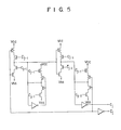
- Fig. 4 shows a detailed arrangement of counter circuit 16.
- Circuit 16 consists of a multi-staged series circuit of (2n-m) binary counters 30, and receives signal ⁇ by counter 30 at the first stage. With this arrangement, upper (n-m)-bit count output signals Cm+1 to Cn are produced as column addresses ICA1 to ICA(n-m).
- binary counter 30 as shown in Fig. 5 is known to those skilled in the art. Referring to Fig. 5, reference symbols Cj-1 and Cj-1 denote count output signals from counter 30 at the immediately preceding stage; and Cj and Cj, count output signals from counter 30 at this stage.
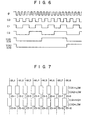
- 8 word lines WL1 to WL8 are provided in memory cell arrays 11A and 11B, and 4 word blocks 23, each including two normal data storage memory cells, are provided along each word line WL.
- the total number of word blocks is 32.
- row addresses RA1 to RA3 (3 bits) are cyclically input from outside the chip at the trailing edge of strobe signal RAS.
- Combinations of levels of 2-bit internal addresses ICA1 and ICA2 are changed every 9th trailing edge of signal RAS. Therefore, as shown in Fig. 6, addresses ICA1 and ICA2 are at LOW levels until the 9th trailing edge of signal RAS. Until that point, as shown in Fig.
- 8 word lines WL1 to WL8 are sequentially selected in accordance with 3-bit row addresses RA1 to RA3, and 8 word blocks 23-1 to 23-8, to which an identical internal column address is assigned, are sequentially selected accordingly.
- Address ICA1 is then kept at HIGH level and address ICA2 is kept at LOW level until the 17th trailing edge of signal RAS. Until that point, 8 word blocks 23-9 to 23-16 defined by these addresses are sequentially selected. Thus, at the 32nd trailing edge of signal RAS, all 32 word blocks in arrays 11A and 11B have been selected.
- the data read operation of the dynamic RAM is performed in accordance with a timing chart shown in Fig. 8. More specifically, this operation begins such that a row address is fetched in the chip at the trailing edge of strobe signal RAS, and a column address is fetched in the chip at the trailing edge of strobe signal CAS .
- write enable signal WE goes to HIGH level at a predetermined timing, and after a predetermined period of time, storage data in a given memory cell defined by a combination of the row and column addresses is produced from output buffer 14 as output data Dout.
- a plurality of word blocks 23 on one word line WL in memory cell arrays 11A and 11B are selected simultaneously, and storage data therein is read out and sensed by amplifier 13.
- Data in one memory cell 21 in one word block 23 of the selected blocks is selected in accordance with column addresses OCA1 to OCAn.
- Data in selected cell 21 is supplied to output buffer 14 through lines 1/0 and I/O and is generated therefrom as data Dout.
- output data Dout is generated from amplifier 13 through lines I/O and I/O before the result of error detection/correction is presented.
- clock signal in the data read mode, clock signal must not be generated from generator 15. Should clock signal ⁇ be generated in this mode, counter circuit 1 6 is undesirably updated and this interrupts regular error detection/correction from word data subsequent to the last data processed in the previous refresh mode.
- the device of this embodiment requires an access time in the data read mode no longer than that in a normal dynamic RAM having no error detection/correction circuit.
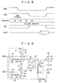
- Fig. 9 shows a detailed arrangement of clock generator 15 which generates clock signal + in synchronism with row address strobe signal RAS in the refresh mode, and does not generate clock signal ⁇ in the normal data read mode.
- Generator 15 has the following arrangement.
- P-channel MOSFET (MOS field effect transistor) 41 and two N-channel MOSFETs 42 and 43 are serially connected between high potential power source Vcc and low potential power source Vss.
- the gate of MOSFET 41 receives potential Vss to be kept ON.
- the gate of MOSFET 42 receives strobe signal RAS through inverter 44.
- the gate of MOSFET 43 receives strobe signal RAS through an even number of inverters (e.g., a series circuit of 4 inverters) 45.
- These MOSFETs 41 to 43 and inverters 44 and 45 constitute pulse generator 46, which generates LOW-level pulse signal RP at the trailing edge of strobe signal RAS.
- MOSFETs 47 to 49 and inverters 50 and 51 constitute pulse generator 52, which generates LOW-level pulse signal CP at the trailing edge of strobe signal CAS.
- Pulse signals RP and CP respectively produced from generators 46 and 52 are input to flip-flop 55 consisting of two NAND gates 53 and 54.
- P-channel MOSFET 56 and three N-channel MOSFETs 57 to 59 are serially inserted between power sources Vcc and Vss.
- the gate of MOSFET 56 receives potential Vss to be kept ON.
- the gate of MOSFET 57 receives output signal Q from flip-flop 55.
- N-channel MOSFET 60 is connected between the gate of MOSFET 57 and power source Vss.
- the gate of MOSFET 60 receives strobe signal RAS through an even number of inverters (e.g., a series circuit of four inverters) 61.
- the gate of MOSFET 58 directly receives strobe signal RAS.
- MOSFET 59 receives strobe signal RAS through an odd number of inverters (e.g., a series circuit of three inverters) 62.
- Clock signal t is generated from a node between MOSFETs 56 and 57.
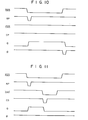
- Figs. 10 and 11 are timing charts showing the operation of clock generator 15 with the arrangement shown in Fig. 9.
- MOSFET 58 When signal RAS then goes to HIGH level, MOSFET 58 is enabled, thus forming the discharging path between the output point of signal ⁇ and power source Vss. The output point of signal ⁇ is then discharged, and signal goes to LOW level. The gate signal from MOSFET 59 goes to LOW level after a predetermined period of time, thereby turning off MOSFET 59. At this time, signal ⁇ goes to HIGH level. The gate signal of MOSFET 60 goes to HIGH level to turn on MOSFET 60. Thereafter, signal Q again goes to LOW level.
- generator 15 generates LOW-level clock signal ⁇ each time signal RAS goes first to LOW level and then to HIGH level.
- both signals RAS and CAS are changed. This corresponds to the data read mode.
- generator 46 when signal RAS goes to LOW level as in Fig. 10, generator 46 generates pulse signal RP in sync therewith. Pulse signal RP causes output signal Q from flip-flop 55 to go to HIGH level. At the next trailing edge of strobe signal CAS, pulse generator 46 generates pulse signal CP. Thus, output signal Q from flip-flop 55 again goes to LOW level, thus turning off MOSFET 57. For this reason, even though signal RAS goes to HIGH level thereafter, the output point of signal ⁇ can no longer be discharged. That is, signal is kept at HIGH level. Therefore, in the data read mode, if signal RAS is changed, clock signal ⁇ is not generated and a count of counter circuit 16 is not updated.
- an external column address When word data is read out from arrays 11A and 11B and an error in the data including an accessed bit is to be detected and corrected, an external column address must have priority over an internal column address.
- signal CAS for example, is used as a switching signal so as to switch column addresses from internal to external.
- the data write mode will now be described with reference to a timing chart shown in Fig. 12,
- the data write operation in the dynamic RAM begins when a row address is fetched in the chip at the trailing edge of signal RAS, and a column address is fetched at the trailing edge of signal CAS.
- write enable signal WE goes to LOW level
- input data Din is written in a memory cell defined by the row and colunm addresses through input buffer 17, encoder circuit 18, and sense amplifier 13.
- Circuit 18 selects one cell data corresponding to upper-bit addresses OCA(n-m+ l ) to 0CAn from addresses OCA1 to 0CAn from the input data, and re-writes the selected data based on other input data. Upon rewritten of the data, data of a check bit in the word data is calculated, and the calculated data is written in the check bit.
- the data write mode In the data write mode, after word data including memory cells specified by the external row and column addresses is read out, it must be rewritten. For this reason, a data write time is prolonged when compared to a conventional dynamic RAM having no error detection/ correction function.
- the data write operation in a dynamic RAM has no access time, unlike the data read operation. More specifically, the data write time is defined only by a cycle time from when signal RAS is set at LOW level until the next data read or write operation begins. Note that this cycle time has a relatively wide margin. Therefore, it can considered that overall, the cycle time is not prolonged when compared with that of the conventional dynamic RAM.
- the circuit shown in Fig. 9 or one equivalent thereto is operated. More specifically, since signal ⁇ is not generated, internal column addresses ICA1 to ICA(n-m) are not changed by counter circuit 16.
- correct data can be output unless the number of errors exceeds the number of bits which can be corrected by an allocated error detection/correction function.
- the data read time is inevitably delayed.
- the data read time is not delayed.
- correct data can be read out unless a soft error occurs upon irradiation of an a ray between the time the data is corrected in the refresh mode and the time it is next read out. It is assumed that the number of soft errors in identical word data will not exceed an error correction limit.
- a data error probability in the device of this embodiment will now be quantitatively analyzed. Since the device of this embodiment corrects data in the refresh mode, the following operation is assumed. The refresh operation is performed with respect to a single memory cell at each time tc (correction time). If data error is found during this operation, it is corrected. The data write operation is performed at each time tw (write time), and the data read operation is performed between two data write operations.
- Probability Pe of data error caused by soft errors is expressed by: where Ps is a probability of soft errors occurring in a memory cell, Rc is a probability of data corrected if a soft error occurs, and Ps is determined by a critical charge for determining HIGH and LOW levels of data in the memory cell, by an impurity concentration profile in a semiconductor substrate immediately under the memory cell, by the flux of an a ray, and by the like.
- the value of Rc is determined by the capacity of an error detection/correction function adopted in the chip.
- Rc, tc, and tw have the following relationships:
- Pe in equation 7 is a probability of readout data error occuring when data is written by a memory device without an error correction circuit, and is read out after time tc has passed. Pe is expressed by equation 8:
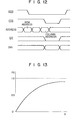
- Fig. 15 shows the relationship between tw/tc and Pe normalized by Pe.
- a function indicated by a broken line is obtained such that probability Pe of readout data errors occuring after time tw/tc has passed from when the data was written by a conventional memory device having no error correction circuit, which is normalized by Pe.
- a slope of this function is 1.
- the error probability increases upon increase in tw/tc.
- the device of this embodiment even if tw/tc increases, the error probability is not increased within the range of tw/tc > 2. Therefore, the error probability is lower than that in the conventional device irrespective of tw/tc.
- the device of this embodiment can provide a significant effect.
- a dynamic RAM requires a refresh operation so as to recover lost storage data due to leakage of a charge accumulated in cells constituted by small capacitors.
- row addresses are periodically and cyclically supplied to raise a potential of word lines.
- storage data in the cells at an identical row address is sensed by a sense amplifier to be temporarily latched, and is rewritten in the original cell to refresh the data. Therefore, the error correction operation can be easily performed together with the refresh operation.
- a static RAM which needs no refresh operation, if row addresses are periodically and cyclically supplied, an operation for correcting an error in word data having a given number of bits can be performed independently in addition to the data read and write operations, without using a refresh operation.
- a semiconductor memory device which can prevent storage data errors due to soft errors from being accumulated and has a data read time, no longer than that of a normal memory device having no error correction function, can be provided.
Landscapes
- Engineering & Computer Science (AREA)
- Theoretical Computer Science (AREA)
- Quality & Reliability (AREA)
- Physics & Mathematics (AREA)
- General Engineering & Computer Science (AREA)
- General Physics & Mathematics (AREA)
- Dram (AREA)
- For Increasing The Reliability Of Semiconductor Memories (AREA)
- Detection And Correction Of Errors (AREA)
- Techniques For Improving Reliability Of Storages (AREA)
Applications Claiming Priority (2)
| Application Number | Priority Date | Filing Date | Title |
|---|---|---|---|
| JP60056515A JPS61214298A (ja) | 1985-03-20 | 1985-03-20 | 誤り訂正機能を備えた半導体記憶装置 |
| JP56515/85 | 1985-03-20 |
Publications (3)
| Publication Number | Publication Date |
|---|---|
| EP0195445A2 true EP0195445A2 (de) | 1986-09-24 |
| EP0195445A3 EP0195445A3 (en) | 1989-01-18 |
| EP0195445B1 EP0195445B1 (de) | 1993-10-06 |
Family
ID=13029257
Family Applications (1)
| Application Number | Title | Priority Date | Filing Date |
|---|---|---|---|
| EP86103788A Expired - Lifetime EP0195445B1 (de) | 1985-03-20 | 1986-03-20 | Halbleiterspeichergerät mit einer Korrekturfunktion |
Country Status (4)
| Country | Link |
|---|---|
| US (1) | US4748627A (de) |
| EP (1) | EP0195445B1 (de) |
| JP (1) | JPS61214298A (de) |
| DE (1) | DE3689128T2 (de) |
Families Citing this family (34)
| Publication number | Priority date | Publication date | Assignee | Title |
|---|---|---|---|---|
| US4916603A (en) * | 1985-03-18 | 1990-04-10 | Wang Labortatories, Inc. | Distributed reference and change table for a virtual memory system |
| JPS623498A (ja) * | 1985-06-28 | 1987-01-09 | Mitsubishi Electric Corp | オンチツプecc回路付半導体記憶装置 |
| JPS62103898A (ja) * | 1985-10-31 | 1987-05-14 | Mitsubishi Electric Corp | ダイナミツクランダムアクセスメモリ装置 |
| JP2514954B2 (ja) * | 1987-03-13 | 1996-07-10 | 三菱電機株式会社 | Icカ−ド |
| JPS6432489A (en) * | 1987-07-27 | 1989-02-02 | Matsushita Electronics Corp | Memory device |
| JPH01183000A (ja) * | 1988-01-14 | 1989-07-20 | Mitsubishi Electric Corp | 誤り訂正回路を有する半導体メモリ装置 |
| US5155834A (en) * | 1988-03-18 | 1992-10-13 | Wang Laboratories, Inc. | Reference and change table storage system for virtual memory data processing system having a plurality of processors accessing common memory |
| JP2534757B2 (ja) * | 1988-07-06 | 1996-09-18 | 株式会社東芝 | リフレッシュ回路 |
| US5128947A (en) * | 1989-06-30 | 1992-07-07 | Motorola, Inc. | Self-checking memory cell array apparatus |
| US5058116A (en) * | 1989-09-19 | 1991-10-15 | International Business Machines Corporation | Pipelined error checking and correction for cache memories |
| US5287363A (en) * | 1991-07-01 | 1994-02-15 | Disk Technician Corporation | System for locating and anticipating data storage media failures |
| US5956352A (en) * | 1992-04-24 | 1999-09-21 | Digital Equipment Corporation | Adjustable filter for error detecting and correcting system |
| US5883903A (en) * | 1993-09-20 | 1999-03-16 | Fujitsu Limited | Semiconductor memory of XN type having parity corresponding to n×m bits |
| US20050036363A1 (en) * | 1996-05-24 | 2005-02-17 | Jeng-Jye Shau | High performance embedded semiconductor memory devices with multiple dimension first-level bit-lines |
| US5748547A (en) * | 1996-05-24 | 1998-05-05 | Shau; Jeng-Jye | High performance semiconductor memory devices having multiple dimension bit lines |
| US7064376B2 (en) * | 1996-05-24 | 2006-06-20 | Jeng-Jye Shau | High performance embedded semiconductor memory devices with multiple dimension first-level bit-lines |
| JPH10177800A (ja) * | 1996-10-21 | 1998-06-30 | Texas Instr Inc <Ti> | エラー訂正ダイナミック・メモリ及びそのエラー訂正方法 |
| US6687860B1 (en) | 1998-01-07 | 2004-02-03 | Matsushita Electric Industrial Co., Ltd. | Data transfer device and data transfer method |
| US6292869B1 (en) | 1998-08-31 | 2001-09-18 | International Business Machines Corporation | System and method for memory scrub during self timed refresh |
| JP2001035158A (ja) * | 1999-07-22 | 2001-02-09 | Nec Corp | メモリアクセス方法及びメモリアクセス方式 |
| US6684353B1 (en) * | 2000-12-07 | 2004-01-27 | Advanced Micro Devices, Inc. | Reliability monitor for a memory array |
| US20030009721A1 (en) * | 2001-07-06 | 2003-01-09 | International Business Machines Corporation | Method and system for background ECC scrubbing for a memory array |
| US20030046630A1 (en) * | 2001-09-05 | 2003-03-06 | Mark Hilbert | Memory using error-correcting codes to correct stored data in background |
| JP4418153B2 (ja) * | 2002-12-27 | 2010-02-17 | 株式会社ルネサステクノロジ | 半導体装置 |
| JP4608235B2 (ja) * | 2004-04-14 | 2011-01-12 | ルネサスエレクトロニクス株式会社 | 半導体記憶装置及び半導体記憶システム |
| JP2006209900A (ja) * | 2005-01-31 | 2006-08-10 | Matsushita Electric Ind Co Ltd | メモリ回路 |
| WO2011062825A2 (en) | 2009-11-20 | 2011-05-26 | Rambus Inc. | Bit-replacement technique for dram error correction |
| US8644104B2 (en) * | 2011-01-14 | 2014-02-04 | Rambus Inc. | Memory system components that support error detection and correction |
| US9691504B2 (en) | 2011-10-24 | 2017-06-27 | Rambus Inc. | DRAM retention test method for dynamic error correction |
| US9411678B1 (en) | 2012-08-01 | 2016-08-09 | Rambus Inc. | DRAM retention monitoring method for dynamic error correction |
| US9734921B2 (en) | 2012-11-06 | 2017-08-15 | Rambus Inc. | Memory repair using external tags |
| US9430324B2 (en) | 2013-05-24 | 2016-08-30 | Rambus Inc. | Memory repair method and apparatus based on error code tracking |
| US10152408B2 (en) | 2014-02-19 | 2018-12-11 | Rambus Inc. | Memory system with activate-leveling method |
| US9495242B2 (en) * | 2014-07-30 | 2016-11-15 | International Business Machines Corporation | Adaptive error correction in a memory system |
Family Cites Families (9)
| Publication number | Priority date | Publication date | Assignee | Title |
|---|---|---|---|---|
| JPS5324741A (en) * | 1976-08-20 | 1978-03-07 | Toshiba Corp | Memory controller |
| US4506362A (en) * | 1978-12-22 | 1985-03-19 | Gould Inc. | Systematic memory error detection and correction apparatus and method |
| JPS55153196A (en) * | 1979-05-14 | 1980-11-28 | Nec Corp | Semiconductor memory |
| US4319356A (en) * | 1979-12-19 | 1982-03-09 | Ncr Corporation | Self-correcting memory system |
| US4380812A (en) * | 1980-04-25 | 1983-04-19 | Data General Corporation | Refresh and error detection and correction technique for a data processing system |
| US4412314A (en) * | 1980-06-02 | 1983-10-25 | Mostek Corporation | Semiconductor memory for use in conjunction with error detection and correction circuit |
| US4493081A (en) * | 1981-06-26 | 1985-01-08 | Computer Automation, Inc. | Dynamic memory with error correction on refresh |
| US4542454A (en) * | 1983-03-30 | 1985-09-17 | Advanced Micro Devices, Inc. | Apparatus for controlling access to a memory |
| US4528665A (en) * | 1983-05-04 | 1985-07-09 | Sperry Corporation | Gray code counter with error detector in a memory system |
-
1985
- 1985-03-20 JP JP60056515A patent/JPS61214298A/ja active Pending
-
1986
- 1986-03-19 US US06/841,436 patent/US4748627A/en not_active Expired - Lifetime
- 1986-03-20 DE DE86103788T patent/DE3689128T2/de not_active Expired - Fee Related
- 1986-03-20 EP EP86103788A patent/EP0195445B1/de not_active Expired - Lifetime
Also Published As
| Publication number | Publication date |
|---|---|
| JPS61214298A (ja) | 1986-09-24 |
| EP0195445B1 (de) | 1993-10-06 |
| EP0195445A3 (en) | 1989-01-18 |
| US4748627A (en) | 1988-05-31 |
| DE3689128D1 (de) | 1993-11-11 |
| DE3689128T2 (de) | 1994-04-07 |
Similar Documents
| Publication | Publication Date | Title |
|---|---|---|
| US4748627A (en) | Semiconductor memory device with an error correction function | |
| US7328377B1 (en) | Error correction for programmable logic integrated circuits | |
| EP1255197B1 (de) | System und Verfahren zur Korrektur von "Soft"-Fehlern in Speicheranordnungen mit wahlfreiem Zugriff | |
| US6233717B1 (en) | Multi-bit memory device having error check and correction circuit and method for checking and correcting data errors therein | |
| US4319356A (en) | Self-correcting memory system | |
| US4958352A (en) | Semiconductor memory device with error check and correcting function | |
| US4139148A (en) | Double bit error correction using single bit error correction, double bit error detection logic and syndrome bit memory | |
| US20140189475A1 (en) | Error detection and correction scheme for a memory device | |
| EP0837392A1 (de) | Speicheranordnung mit einer Fehlerkorrekturfunktion | |
| US4453251A (en) | Error-correcting memory with low storage overhead and fast correction mechanism | |
| US8365036B2 (en) | Soft error correction in a memory array and method thereof | |
| US5533194A (en) | Hardware-assisted high speed memory test apparatus and method | |
| EP0600137A1 (de) | Verfahren und Einrichtung zur Korrektur von Fehlern in einem Speicher | |
| JP2669303B2 (ja) | ビットエラー訂正機能付き半導体メモリ | |
| US7765455B2 (en) | Semiconductor memory device | |
| US9280418B2 (en) | Memory device implementing reduced ECC overhead | |
| US7509561B2 (en) | Parity checking circuit for continuous checking of the parity of a memory cell | |
| US7746692B2 (en) | Multiple-level memory with analog read | |
| EP0424301A2 (de) | Mit Datenauffrischung überlappende Dabenschrubben | |
| KR20070026075A (ko) | 반도체 집적 회로 장치 | |
| US20040187050A1 (en) | Test structure and method for accurate determination of soft error of logic components | |
| US20030046630A1 (en) | Memory using error-correcting codes to correct stored data in background | |
| JPS6125177B2 (de) | ||
| JP2007052596A (ja) | ソフトエラー検出回路 | |
| US11769567B2 (en) | Devices and methods for preventing errors and detecting faults within a memory device |
Legal Events
| Date | Code | Title | Description |
|---|---|---|---|
| PUAI | Public reference made under article 153(3) epc to a published international application that has entered the european phase |
Free format text: ORIGINAL CODE: 0009012 |
|
| 17P | Request for examination filed |
Effective date: 19860320 |
|
| AK | Designated contracting states |
Kind code of ref document: A2 Designated state(s): DE FR GB |
|
| PUAL | Search report despatched |
Free format text: ORIGINAL CODE: 0009013 |
|
| AK | Designated contracting states |
Kind code of ref document: A3 Designated state(s): DE FR GB |
|
| 17Q | First examination report despatched |
Effective date: 19901009 |
|
| GRAA | (expected) grant |
Free format text: ORIGINAL CODE: 0009210 |
|
| AK | Designated contracting states |
Kind code of ref document: B1 Designated state(s): DE FR GB |
|
| REF | Corresponds to: |
Ref document number: 3689128 Country of ref document: DE Date of ref document: 19931111 |
|
| ET | Fr: translation filed | ||
| PLBE | No opposition filed within time limit |
Free format text: ORIGINAL CODE: 0009261 |
|
| STAA | Information on the status of an ep patent application or granted ep patent |
Free format text: STATUS: NO OPPOSITION FILED WITHIN TIME LIMIT |
|
| 26N | No opposition filed | ||
| PGFP | Annual fee paid to national office [announced via postgrant information from national office to epo] |
Ref country code: DE Payment date: 19970401 Year of fee payment: 12 |
|
| PGFP | Annual fee paid to national office [announced via postgrant information from national office to epo] |
Ref country code: GB Payment date: 19980311 Year of fee payment: 13 |
|
| PG25 | Lapsed in a contracting state [announced via postgrant information from national office to epo] |
Ref country code: DE Free format text: LAPSE BECAUSE OF NON-PAYMENT OF DUE FEES Effective date: 19981201 |
|
| REG | Reference to a national code |
Ref country code: FR Ref legal event code: D6 |
|
| PG25 | Lapsed in a contracting state [announced via postgrant information from national office to epo] |
Ref country code: GB Free format text: LAPSE BECAUSE OF NON-PAYMENT OF DUE FEES Effective date: 19990320 |
|
| GBPC | Gb: european patent ceased through non-payment of renewal fee |
Effective date: 19990320 |
|
| PGFP | Annual fee paid to national office [announced via postgrant information from national office to epo] |
Ref country code: FR Payment date: 20050308 Year of fee payment: 20 |