EP0193177A2 - Berührungsaktive Eingabevorrichtung - Google Patents
Berührungsaktive Eingabevorrichtung Download PDFInfo
- Publication number
- EP0193177A2 EP0193177A2 EP86102468A EP86102468A EP0193177A2 EP 0193177 A2 EP0193177 A2 EP 0193177A2 EP 86102468 A EP86102468 A EP 86102468A EP 86102468 A EP86102468 A EP 86102468A EP 0193177 A2 EP0193177 A2 EP 0193177A2
- Authority
- EP
- European Patent Office
- Prior art keywords
- input device
- touch input
- data
- character code
- touch
- Prior art date
- Legal status (The legal status is an assumption and is not a legal conclusion. Google has not performed a legal analysis and makes no representation as to the accuracy of the status listed.)
- Withdrawn
Links
Images


Classifications
-
- G—PHYSICS
- G06—COMPUTING; CALCULATING OR COUNTING
- G06F—ELECTRIC DIGITAL DATA PROCESSING
- G06F3/00—Input arrangements for transferring data to be processed into a form capable of being handled by the computer; Output arrangements for transferring data from processing unit to output unit, e.g. interface arrangements
- G06F3/01—Input arrangements or combined input and output arrangements for interaction between user and computer
- G06F3/03—Arrangements for converting the position or the displacement of a member into a coded form
- G06F3/041—Digitisers, e.g. for touch screens or touch pads, characterised by the transducing means
- G06F3/045—Digitisers, e.g. for touch screens or touch pads, characterised by the transducing means using resistive elements, e.g. a single continuous surface or two parallel surfaces put in contact
-
- G—PHYSICS
- G06—COMPUTING; CALCULATING OR COUNTING
- G06F—ELECTRIC DIGITAL DATA PROCESSING
- G06F3/00—Input arrangements for transferring data to be processed into a form capable of being handled by the computer; Output arrangements for transferring data from processing unit to output unit, e.g. interface arrangements
- G06F3/01—Input arrangements or combined input and output arrangements for interaction between user and computer
- G06F3/02—Input arrangements using manually operated switches, e.g. using keyboards or dials
- G06F3/0202—Constructional details or processes of manufacture of the input device
- G06F3/021—Arrangements integrating additional peripherals in a keyboard, e.g. card or barcode reader, optical scanner
Definitions
- This invention relates to a touch input device having a touch pad, and nore particularly to an improved touch input device adapted to detect a coordinates data corresponding to the position of the touch pad touched by a stylus or finger.
- a touch input device has been primarily utilized to input analog date such as figures into a display of a central processing unit (CPU).
- the conventional touch input device designed to input such analog data cannot input digital data i,e,alphanumeric codes.
- a key pad is required in addition to the touch input device.
- the key pad is provided, there is caused a problen that the size of a key board including the touch input device and key pad necessarily expands due to the added space of the key pad.
- a prisary object of this invention to provide a touch input device capable of inputting not only analog data but digital data by switching an input Mode.
- a touch input device comprising a touch pad, means for detecting a coordinates data corresponding to the position of the touch pad to be touched, means for converting the coordinates data into a character code, and means for selectively designating either the coordinates data or the character code as an output data.
- a touch input device 11 is built in a keyboard 10 provided with a plurality of keys 12.
- the keyboard is connected to a CRT display unit 13 on which various figures and character codes are displayed according to the input operation from the keyboard 12.
- a key 12a is provided for switching an input Mode into either analog data input Mode or digital data input Mode.
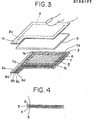
- the touch input device 11 comprises conductor 2 printed on the under surface of an outside sheet 1, pressure sensitive conductor 5, and resistance 4 printed over an inside sheet 3.
- the outside sheet 1 is made of polyethylene terephthalate ( PET ) film the thickness of which is approximately 100 micron.
- the printed conductor 2 is made of semirectangular silver pattern whose lead pattern 2a is printed on a connector portion la.
- the outer surface of outside sheet 1 is printed to display alphanumeric characters ( Fig. 2). Such characters may be also printed on the inside sheet 3 Instead of outside sheet 1.
- the pressure sensitive conductor 5 is made of semirectangular anisotrophic pressure sensitive conductive rubber sheet which will serve as a conductor when a force is applied in its thickness direction.
- the inside sheet 3 is also made of 100 aicron thick PET fila which has semirectansular resistance 4 printed on the surface firmly contacting with the conductor 5.
- the resistance 4 comprises central portion 6 which is made of carbon pattern having uniform resistance value, and marginal electrode portion 7 which is also made of carbon pattern having a constant width and uniform resistance value thereon.
- the sheet 3 has a connector portion 3a on which lead patterns 8a,8b,8c, and 8d extend from the respective corners 7a,7b,7c, and 7d of the marginal electrode portion 7.
- the central portion 8 has a resistance value of several kiloohas/square while the marginal electrode portion 7 has a resistance value of tens of ohms/square.
- the lead patterns 8a through 8d have an insulating naterial (not shown) provided thereon.
- conductor 2 is connected through a flexible printed circuit board (not shown) to a converter 22 and operation circuit 23.
- the V-F converter 22 provides pulses whose frequency is proportional to an input voltage.
- the operation circuit 23 counts the pulses output from the converter 22 for a given t iae and provides a CPU 24 with the counted value as a coordinates data.
- the CPU performs an operation which will be described hereinafter.
- the corner portions 7a and 7b of marsinal electrode portion 7 are connected through a flexible printed circuit board (not shawn) to ground, an analog switch 21 respectively.
- the corner portions 7c and 7d are connected to a power source Vcc and the analog switch 21 respectively as shown in Fig. 5.
- the analog switch 21 alternately connects the corner portion 7b and 7d either to the power source Vcc or ground.
- the corner portions 7a and 7c are respectively connected to ground and Vcc, while the corner portions 7b and 7d are respectively connected to ground and Vcc through the analog switch 21.
- the side 9a between the corner portions 7a and 7b of marginal electrode portion 7 has a voltage close to ground
- the side 9c between the corner portions 7c and 7d has a voltage close to power source Vcc.
- the central portion 6 has a potential gradient from the side 9a to side 9c.
- the side 9d between the corner portion 7a and 7d, and side 9b between the corner portion 7b and 7c have potential gradients from ground to Vcc respectively, thereby correcting the distortion of the potential gradient in the marginal portion of the central portion 6.
- the pressure sensitive conductor 5 establishes a conductive path on the position being depressed and the potential at the depressed position is input through conductor 2 to V-F converter 22 which outputs to operation circuit 23 pulses whose frequency is proportional to the potential.
- the operation circuit 23 as previously described. counts the input pulses for a given time and provides a CPU 24 with the counted value as an abscissa data.
- analog switch 21 Upon receipt of X-Y switching signal from CPU 24, analog switch 21 will operate so that the corner portions 7b and 7d are respectively connected to Vcc and ground. As a result, the side 9d between the corner portions 7a and 7d has a value close to ground, while the side 9b between the corner portions 7b and 7c has a value close to Vce. Accordingly, the central portion 6 has a potential gradient from the side 9d to side 9b. In addition. the side 9a between the corner portions 7a and 7b and the side 9c between the corner portions 7d and 7c have potential gradients from ground to Vcc, thereby correcting the distortion of the potential gradient In the marginal portion of central portion 6.
- the converter 22 When the potential of the depressed position is input through conductor 2 to V-F converter 22, the converter 22 outputs pulses whose frequency is proportional to the potential.
- the operation circuit 23 counts the pulses output from converter 22 for a given time and provides CPU 24 with the counted value as an ordinate data.
- an abscissa data and ordinate data can be alternately detected by changing the direction of a potential gradient to be established using an analog switch which is operated by X-Y switching sisnal.
- the switching period is so short that the delay of detection timing is negligible. Consequently, the abscissa and ordinate data of the position being depressed can be almost simultaneously detected.
- steps IS and 2S an abscissa and ordinate data are input by touching any position of touch pad 11, corresponding to the position being touched. Then, it is inquired whether analog data is to be output, that is, coordinate data is to be output in step 3S. If an analog data input Mode has been set by key 12s, a sequence flows to steps 4S and 5S in which the abscissa and ordinate data are output to a host computer (not shown ) which is located in CRT display unit 13 for displaying an analog data on the basis of the coordinates data.
- a sequence flows to steps 6S and 7S, wherein a row data A and line data B are calculated based on the abscissa and ordinate data.
- MX and nx represent the maximum abscissa data and the maximum row number of characters respectively (step 6S ).
- MY and ny represent the maximum ordinate data and the maximus line number of characters respectively.
- a character code C is located (step 8S ) and output to host computer 24( step 9S ) which displays a character based on the character code C on display unit 13.
- characters are printed on the surface of the outside sheet 1.
- the touch input device may be designed to allow such characters to appear only when a digital input Mode is selected by key 12a. This function can be performed by using liquid crystal display or light-emitting diodes.
- A-D converter can be employed instead of V-F converter to detect coordinates data.
- pressure sensitive conductor 5 aay be printed over either conductor 2 or resistance 4.
- outside sheet 1 and inside sheet 3 may be integrally formed so that when folded, they confront each other.
Applications Claiming Priority (2)
| Application Number | Priority Date | Filing Date | Title |
|---|---|---|---|
| JP27716/85U | 1985-02-26 | ||
| JP1985027716U JPS61143241U (de) | 1985-02-26 | 1985-02-26 |
Publications (2)
| Publication Number | Publication Date |
|---|---|
| EP0193177A2 true EP0193177A2 (de) | 1986-09-03 |
| EP0193177A3 EP0193177A3 (de) | 1990-04-18 |
Family
ID=12228727
Family Applications (1)
| Application Number | Title | Priority Date | Filing Date |
|---|---|---|---|
| EP86102468A Withdrawn EP0193177A3 (de) | 1985-02-26 | 1986-02-26 | Berührungsaktive Eingabevorrichtung |
Country Status (2)
| Country | Link |
|---|---|
| EP (1) | EP0193177A3 (de) |
| JP (1) | JPS61143241U (de) |
Cited By (5)
| Publication number | Priority date | Publication date | Assignee | Title |
|---|---|---|---|---|
| GB2184274B (en) * | 1985-11-18 | 1989-10-25 | Canon Kk | Image forming apparatus |
| DE4222940A1 (de) * | 1992-07-11 | 1994-01-13 | Dyna Systems Gmbh | Tastatur mit Maus-Eingabefeld |
| EP0672980A2 (de) * | 1994-03-18 | 1995-09-20 | International Business Machines Corporation | Verbindung einer Tastatur und eines berührungsempfindlichen Tablett in einem zweiteiligen Gehäuse |
| FR2735592A1 (fr) * | 1995-06-19 | 1996-12-20 | Samsung Display Devices Co Ltd | Dispositif d'entree a entrees multiples |
| EP2411893A2 (de) * | 2009-03-25 | 2012-02-01 | Peratech Limited | Sensor |
Families Citing this family (2)
| Publication number | Priority date | Publication date | Assignee | Title |
|---|---|---|---|---|
| JPH1157212A (ja) * | 1997-08-24 | 1999-03-02 | Sony Computer Entertainment:Kk | ゲーム装置、ゲーム機用操作装置、ゲームシステム及びゲーム装置の双方向通信方法 |
| TW389918B (en) | 1997-08-24 | 2000-05-11 | Sony Computer Entertainment Inc | Game apparatus, game machine manipulation device, game system and interactive communication method for game apparatus |
Citations (4)
| Publication number | Priority date | Publication date | Assignee | Title |
|---|---|---|---|---|
| US4224615A (en) * | 1978-09-14 | 1980-09-23 | Texas Instruments Incorporated | Method of using a liquid crystal display device as a data input device |
| US4313108A (en) * | 1978-12-07 | 1982-01-26 | Casio Computer Co., Ltd. | Electric apparatus for displaying a plurality of key symbols on a single passive display |
| US4345248A (en) * | 1979-12-14 | 1982-08-17 | Citizen Watch Company Limited | Liquid crystal display device with write-in capability |
| JPS57157337A (en) * | 1981-03-25 | 1982-09-28 | Nippon Telegr & Teleph Corp <Ntt> | Information input tablet |
Family Cites Families (2)
| Publication number | Priority date | Publication date | Assignee | Title |
|---|---|---|---|---|
| JPS50126125A (de) * | 1974-03-22 | 1975-10-03 | ||
| JPS5793431A (en) * | 1980-11-30 | 1982-06-10 | Pentel Kk | Character information input device |
-
1985
- 1985-02-26 JP JP1985027716U patent/JPS61143241U/ja active Pending
-
1986
- 1986-02-26 EP EP86102468A patent/EP0193177A3/de not_active Withdrawn
Patent Citations (4)
| Publication number | Priority date | Publication date | Assignee | Title |
|---|---|---|---|---|
| US4224615A (en) * | 1978-09-14 | 1980-09-23 | Texas Instruments Incorporated | Method of using a liquid crystal display device as a data input device |
| US4313108A (en) * | 1978-12-07 | 1982-01-26 | Casio Computer Co., Ltd. | Electric apparatus for displaying a plurality of key symbols on a single passive display |
| US4345248A (en) * | 1979-12-14 | 1982-08-17 | Citizen Watch Company Limited | Liquid crystal display device with write-in capability |
| JPS57157337A (en) * | 1981-03-25 | 1982-09-28 | Nippon Telegr & Teleph Corp <Ntt> | Information input tablet |
Non-Patent Citations (3)
| Title |
|---|
| IBM Technical Disclosure Bulletin, New York (US) Vol 14, No 3, August 1971 "Keyboard for electronic tablet or digitizer" R.N. Wolfe, p 807-808 * |
| IBM Technical Disclosure Bulletin, New York, (US) Vol 27, No 1A, June 1984 "Touch-sensitive screen proximate and electronically composable display" D.B. Hildebrand, p 43-44 * |
| PATENT ABSTRACTS OF JAPAN, Vol 6, No 262, P-164, (1140) December 21, 1982; & JP 57157337 A [Nippon Denshin Denwa Kosha] 28.9.1982 * |
Cited By (6)
| Publication number | Priority date | Publication date | Assignee | Title |
|---|---|---|---|---|
| GB2184274B (en) * | 1985-11-18 | 1989-10-25 | Canon Kk | Image forming apparatus |
| DE4222940A1 (de) * | 1992-07-11 | 1994-01-13 | Dyna Systems Gmbh | Tastatur mit Maus-Eingabefeld |
| EP0672980A2 (de) * | 1994-03-18 | 1995-09-20 | International Business Machines Corporation | Verbindung einer Tastatur und eines berührungsempfindlichen Tablett in einem zweiteiligen Gehäuse |
| EP0672980A3 (de) * | 1994-03-18 | 1995-12-06 | Ibm | Verbindung einer Tastatur und eines berührungsempfindlichen Tablett in einem zweiteiligen Gehäuse. |
| FR2735592A1 (fr) * | 1995-06-19 | 1996-12-20 | Samsung Display Devices Co Ltd | Dispositif d'entree a entrees multiples |
| EP2411893A2 (de) * | 2009-03-25 | 2012-02-01 | Peratech Limited | Sensor |
Also Published As
| Publication number | Publication date |
|---|---|
| EP0193177A3 (de) | 1990-04-18 |
| JPS61143241U (de) | 1986-09-04 |
Similar Documents
| Publication | Publication Date | Title |
|---|---|---|
| US4587378A (en) | Two-layer touch tablet | |
| US5521336A (en) | Simplified digital pad sensor | |
| US5543589A (en) | Touchpad with dual sensor that simplifies scanning | |
| JP4038480B2 (ja) | 二重機能入力装置および方法 | |
| US7952564B2 (en) | Multiple-touch sensor | |
| ES2362268T3 (es) | Detector de proximidad de entradas múltiples y sistema de panel táctil. | |
| EP0976096B1 (de) | Umsetzer für widerstandsberuhrungsbildschirme | |
| KR101101581B1 (ko) | 멀티 포인트 터치 감지 장치 | |
| US20090002338A1 (en) | Screen input type image display | |
| US6738048B1 (en) | Touch screen controller | |
| US20080028309A1 (en) | Input device | |
| JP3069949B2 (ja) | 射出成形機の入力装置 | |
| US7339124B2 (en) | Input key and input apparatus | |
| EP3936983A1 (de) | System zur erkennung eines angeklickten zustands und eines nicht angeklickten zustands einer taste für eine kapazitive berührungsvorrichtung | |
| JPH08137607A (ja) | 座標入力装置 | |
| US4184147A (en) | Input device for input of alphanumeric characters into a computer | |
| EP0193177A2 (de) | Berührungsaktive Eingabevorrichtung | |
| JPH09212302A (ja) | 座標入力装置 | |
| JPH0619849A (ja) | 携帯型電子機器、および位置検出装置で用いる位置指示器 | |
| JP2001043003A (ja) | タッチパネル入力装置 | |
| JP2635473B2 (ja) | 電子機器 | |
| JPS61237126A (ja) | キ−ボ−ド | |
| JP2809930B2 (ja) | データ入力用キー装置 | |
| JPS61241823A (ja) | タツチ入力装置 | |
| JPS605008B2 (ja) | スイッチ断接型座標入力装置 |
Legal Events
| Date | Code | Title | Description |
|---|---|---|---|
| PUAI | Public reference made under article 153(3) epc to a published international application that has entered the european phase |
Free format text: ORIGINAL CODE: 0009012 |
|
| 17P | Request for examination filed |
Effective date: 19860226 |
|
| AK | Designated contracting states |
Kind code of ref document: A2 Designated state(s): AT BE CH DE FR GB IT LI LU NL SE |
|
| PUAL | Search report despatched |
Free format text: ORIGINAL CODE: 0009013 |
|
| AK | Designated contracting states |
Kind code of ref document: A3 Designated state(s): AT BE CH DE FR GB IT LI LU NL SE |
|
| STAA | Information on the status of an ep patent application or granted ep patent |
Free format text: STATUS: THE APPLICATION IS DEEMED TO BE WITHDRAWN |
|
| 18D | Application deemed to be withdrawn |
Effective date: 19910928 |
|
| RIN1 | Information on inventor provided before grant (corrected) |
Inventor name: YAMASHITA, TERUFUMI |