EP0193093B1 - Primärseitig getakteter Eintaktdurchflusswandler - Google Patents
Primärseitig getakteter Eintaktdurchflusswandler Download PDFInfo
- Publication number
- EP0193093B1 EP0193093B1 EP86102142A EP86102142A EP0193093B1 EP 0193093 B1 EP0193093 B1 EP 0193093B1 EP 86102142 A EP86102142 A EP 86102142A EP 86102142 A EP86102142 A EP 86102142A EP 0193093 B1 EP0193093 B1 EP 0193093B1
- Authority
- EP
- European Patent Office
- Prior art keywords
- switch
- winding
- iii
- secondary winding
- changeover
- Prior art date
- Legal status (The legal status is an assumption and is not a legal conclusion. Google has not performed a legal analysis and makes no representation as to the accuracy of the status listed.)
- Expired
Links
- 238000004804 winding Methods 0.000 claims abstract description 32
- 239000003990 capacitor Substances 0.000 claims abstract description 11
- 238000009499 grossing Methods 0.000 claims abstract description 7
- 239000004065 semiconductor Substances 0.000 claims description 2
- 238000012544 monitoring process Methods 0.000 description 5
- 238000010586 diagram Methods 0.000 description 3
- 230000005347 demagnetization Effects 0.000 description 2
- 230000001419 dependent effect Effects 0.000 description 2
- 230000001105 regulatory effect Effects 0.000 description 2
- 238000004891 communication Methods 0.000 description 1
- 238000010276 construction Methods 0.000 description 1
- 238000011161 development Methods 0.000 description 1
- 230000018109 developmental process Effects 0.000 description 1
- 238000007599 discharging Methods 0.000 description 1
- 230000017525 heat dissipation Effects 0.000 description 1
- 229920006395 saturated elastomer Polymers 0.000 description 1
Images

Classifications
-
- H—ELECTRICITY
- H02—GENERATION; CONVERSION OR DISTRIBUTION OF ELECTRIC POWER
- H02M—APPARATUS FOR CONVERSION BETWEEN AC AND AC, BETWEEN AC AND DC, OR BETWEEN DC AND DC, AND FOR USE WITH MAINS OR SIMILAR POWER SUPPLY SYSTEMS; CONVERSION OF DC OR AC INPUT POWER INTO SURGE OUTPUT POWER; CONTROL OR REGULATION THEREOF
- H02M3/00—Conversion of DC power input into DC power output
- H02M3/22—Conversion of DC power input into DC power output with intermediate conversion into AC
- H02M3/24—Conversion of DC power input into DC power output with intermediate conversion into AC by static converters
- H02M3/28—Conversion of DC power input into DC power output with intermediate conversion into AC by static converters using discharge tubes with control electrode or semiconductor devices with control electrode to produce the intermediate AC
- H02M3/325—Conversion of DC power input into DC power output with intermediate conversion into AC by static converters using discharge tubes with control electrode or semiconductor devices with control electrode to produce the intermediate AC using devices of a triode or a transistor type requiring continuous application of a control signal
- H02M3/335—Conversion of DC power input into DC power output with intermediate conversion into AC by static converters using discharge tubes with control electrode or semiconductor devices with control electrode to produce the intermediate AC using devices of a triode or a transistor type requiring continuous application of a control signal using semiconductor devices only
- H02M3/33561—Conversion of DC power input into DC power output with intermediate conversion into AC by static converters using discharge tubes with control electrode or semiconductor devices with control electrode to produce the intermediate AC using devices of a triode or a transistor type requiring continuous application of a control signal using semiconductor devices only having more than one ouput with independent control
-
- H—ELECTRICITY
- H02—GENERATION; CONVERSION OR DISTRIBUTION OF ELECTRIC POWER
- H02M—APPARATUS FOR CONVERSION BETWEEN AC AND AC, BETWEEN AC AND DC, OR BETWEEN DC AND DC, AND FOR USE WITH MAINS OR SIMILAR POWER SUPPLY SYSTEMS; CONVERSION OF DC OR AC INPUT POWER INTO SURGE OUTPUT POWER; CONTROL OR REGULATION THEREOF
- H02M1/00—Details of apparatus for conversion
- H02M1/0003—Details of control, feedback or regulation circuits
- H02M1/0032—Control circuits allowing low power mode operation, e.g. in standby mode
-
- H—ELECTRICITY
- H02—GENERATION; CONVERSION OR DISTRIBUTION OF ELECTRIC POWER
- H02M—APPARATUS FOR CONVERSION BETWEEN AC AND AC, BETWEEN AC AND DC, OR BETWEEN DC AND DC, AND FOR USE WITH MAINS OR SIMILAR POWER SUPPLY SYSTEMS; CONVERSION OF DC OR AC INPUT POWER INTO SURGE OUTPUT POWER; CONTROL OR REGULATION THEREOF
- H02M7/00—Conversion of AC power input into DC power output; Conversion of DC power input into AC power output
- H02M7/02—Conversion of AC power input into DC power output without possibility of reversal
- H02M7/04—Conversion of AC power input into DC power output without possibility of reversal by static converters
- H02M7/05—Capacitor coupled rectifiers
-
- Y—GENERAL TAGGING OF NEW TECHNOLOGICAL DEVELOPMENTS; GENERAL TAGGING OF CROSS-SECTIONAL TECHNOLOGIES SPANNING OVER SEVERAL SECTIONS OF THE IPC; TECHNICAL SUBJECTS COVERED BY FORMER USPC CROSS-REFERENCE ART COLLECTIONS [XRACs] AND DIGESTS
- Y02—TECHNOLOGIES OR APPLICATIONS FOR MITIGATION OR ADAPTATION AGAINST CLIMATE CHANGE
- Y02B—CLIMATE CHANGE MITIGATION TECHNOLOGIES RELATED TO BUILDINGS, e.g. HOUSING, HOUSE APPLIANCES OR RELATED END-USER APPLICATIONS
- Y02B70/00—Technologies for an efficient end-user side electric power management and consumption
- Y02B70/10—Technologies improving the efficiency by using switched-mode power supplies [SMPS], i.e. efficient power electronics conversion e.g. power factor correction or reduction of losses in power supplies or efficient standby modes
Definitions
- the invention relates to a single-ended forward converter clocked on the primary side according to the features of the preamble of claim 1.
- Communication terminals which are suitable for so-called integrated services, are characterized above all by a compact shape, so that they can be placed on any desk, and the main components, such as keyboard and telephone receiver with storage, can be positioned and used independently of one another.
- the associated power supply must be housed in a relatively narrow space, which poses problems with heat dissipation but also with the dimensions of the power supply.
- the power supply must provide several different output voltages, and depending on the particular mode of operation - full operation or provisional operation - all output voltages or only a part of these output voltages must be available at the same time.
- a switching power supply with several output circuits is known for example from EP-A-111 365, wherein individual output circuits can be switched off if necessary. Switching off an output circuit with the aid of a switch in a power supply device which also has a plurality of output circuits is also known from EP-A-0 048 934.
- the present invention is based on the object of designing a single-ended flow converter clocked on the primary side of the type mentioned in the preamble of claim 1 in such a way that the output circuits, depending on the operating mode - full operation and / or auxiliary operation - can be switched on and off with simple means and also connected to one another can be that the circuit complexity for providing several independent output voltages can be kept as low as possible with optimal use of the individual circuit components.
- a single-ended forward converter is obtained, in which DC voltages that are not required can be switched off in the auxiliary mode.
- the fact that all the main components of the circuit are used both in full operation and in auxiliary operation can save component costs and volume. In addition, high efficiency and high reliability of the circuit are achieved.
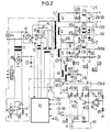
- the primary side PD of the flow converter and the control and monitoring module RÜ are shown as a block diagram.
- the primary winding 1 of the transformer T3 feeds three secondary windings 11, 111, IV, which are followed by output circuits according to the flow principle.
- Each output circuit has a rectifier diode V17, V18, V19, V20, the associated storage inductor Ll a, L1b, .L2a, L2b, the freewheeling diode V9, V8, V7, V6 and the first smoothing capacitors C3, C4, C5, C6.
- the rectifier diodes are connected in series to the storage choke, the freewheeling diode is parallel to this.
- the voltages U1, U2, U3 and U4, which feed the loads VA, VB, VC and VD, are present at the outputs of the output circuits 1, 2, 3,4.
- a switch K1 is located between the beginning of the first secondary winding II and the end of the second secondary winding 111, while the live output of the first output circuit 1 is connected to a first changeover contact of a changeover switch K2 via an ohmic resistor R5.
- the second changeover contact of the changeover switch K2 is routed via a second ohmic resistor R6 to the storm-leading output of the second secondary winding III of the first transformer T3.
- the two changeover contacts have a common contact of the changeover switch K2 both connected to the input of the control and monitoring module RÜ and to ground via a third ohmic resistor R9.
- the second secondary winding 111 of the first transformer T3 has a rectifier diode V18, V19, both at the start of the winding and at the end of its winding, to which corresponding storage chokes L2a and L2b are connected.
- This construction enables two consumers to be fed simultaneously and, in combination with the switch K1, the second consumer VB and the third consumer VC to be switched off.
- the voltages that cannot be switched off are generated in parallel operation.
- the switch K1 is open and the changeover switch K2 connects the resistor R5 to R9.
- the voltage for the first consumer VA (5 volts) is regulated in this case.
- the switch K1 is closed during full operation, the changeover switch K2 connects the resistor R6 with the resistor R9. In this case, the voltage of the third consumer VC (12 volts) regulated.
- the transformer T1 connected in parallel to the line rectifier V1 serves to supply the control and monitoring circuit RÜ when switched on and in parallel operation.
- the control and monitoring circuit RÜ is supplied by the above-mentioned voltage with the aid of the first diode V13 in certain operating states.
- the current converter T5 monitors the current flowing in the primary circuit. If the current exceeds the allowable limit, e.g. B. in the event of a short circuit at the output, the control signals for the switching transistors V4 and V5 are blocked and the power supply is switched off via the monitoring logic. Switching on again takes place by switching the network off and on again.
- the switch K1 and the changeover switch K2 in the arrangement according to FIG. 1 are implemented in the technical embodiment by semiconductors, namely the switch K1 by a MOS transistor V10 and the changeover switch K2 by an integrated circuit.
- the switch K1 in the form of a MOS transistor V10 is electrically isolated by the first secondary winding WII of the third transformer T4 with subsequent rectification by the second diode V11 and smoothing of the alternating voltage with the second capacitor C7.
- the AC fan of the power supply is connected in a similar manner to the mains AC voltage by the second secondary winding Will of the third transformer T4, by the third diode V12, the third smoothing capacitor C8, the first transistor V16 and the bridge rectifier V15.
- the primary winding WI of the third transformer T4 is switched on by the transistor N1 / 1, which is located in the above-mentioned integrated circuit IC, to the square-wave AC voltage of the first secondary winding II of the first transformer T3.
- the fourth diode V21 enables a reliable demagnetization of the third transformer T4.
- the voltages of the second and third consumers VB, VC are slowly switched on with the MOS transistor V10 in order to prevent the current limitation from responding.
- the switch-on time is determined by the second capacitor C7 and the ohmic resistor R12.
- the function of the changeover switch K2 in the circuit arrangement according to FIG. 1 is carried out by the circuit designed as an IC with the transistors N1 / 2, N1 / 3 and N1 / 4.
- This circuit is controlled by the operational amplifier N2.
- the reference voltage U H which is generated in the control module RÜ, is present at the negative input of the operational amplifier N2.
- the output voltage of the third consumer VC (12 volts) is supplied using the resistance divider R10, R11. If the arrangement is operated in auxiliary mode, the output of the operational amplifier is at the 0 volt potential.
- the fourth transistor N1 / 4 of the integrated circuit is thus blocked.
- the second transistor N1 / 2 of the integrated circuit is operated in a saturated state by the base resistor R4 located at the output for the first consumer VA.
- the voltage for the first consumer VA (5 volts NA) is supplied to the control circuit as the actual value.
- the voltages for the second and third consumers VB, VC (5 volts and 12 volts) slowly ramp up.
- the output of the operational amplifier N2 switches to H shortly before the output voltage for the third consumer reaches the target voltage (12 volts).
- the third and fourth transistors N1 / 3 and N1 / 4 of the integrated circuit IC become conductive and the second transistor N1 / 2 of the integrated circuit is blocked.
- the actual value for the control module is generated from the voltage for the third consumer VC via the other resistor divider with the resistors R6, R9.
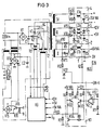
- the flow converter according to FIG 3 has the same technical properties as that described in FIG 2.
- the potential-free control of the MOS transistor V10 described in FIG. 2 is achieved in the arrangement according to FIG. 3 by the galvanically coupled circuit with the second transistor V22, the fourth ohmic resistor R12, the second capacitor C7 and the second ohmic resistor R1 replaced.
- the signal ON-H is used to control the second transistor V22, which is operated in the basic circuit and operates as a constant current source.
- the source electrode of the MOS transistor V10 becomes negative.
- the second capacitor C7 is slowly charged via the fourth ohmic resistor R12.
- the MOS transistor V10 becomes conductive.
- the second diode V11 prevents the second capacitor C7 from discharging if the gate electrode of the MOS transistor V10 becomes positive during the current flow time.
- a second winding on the mains transformer T1 is required to supply the fan Lf.
- the primary-side design of the flow converter corresponds completely to that according to FIG. 2.
- the output voltage can be adapted to different load ranges by selecting diodes with different lock voltages.
- the voltage-dependent control loop changeover is important for switching on in full operation, and the immediate changeover of the control loop to + 5V NA is important for switching over to auxiliary operation.
- the voltage-dependent control loop switchover to avoid overvoltages or undervoltages is important for switching the operating states.
Landscapes
- Engineering & Computer Science (AREA)
- Power Engineering (AREA)
- Dc-Dc Converters (AREA)
- Amplifiers (AREA)
- Control Of High-Frequency Heating Circuits (AREA)
Priority Applications (1)
| Application Number | Priority Date | Filing Date | Title |
|---|---|---|---|
| AT86102142T ATE43761T1 (de) | 1985-02-25 | 1986-02-19 | Primaerseitig getakteter eintaktdurchflusswandler. |
Applications Claiming Priority (2)
| Application Number | Priority Date | Filing Date | Title |
|---|---|---|---|
| DE3506575 | 1985-02-25 | ||
| DE3506575 | 1985-02-25 |
Publications (3)
| Publication Number | Publication Date |
|---|---|
| EP0193093A2 EP0193093A2 (de) | 1986-09-03 |
| EP0193093A3 EP0193093A3 (en) | 1987-09-09 |
| EP0193093B1 true EP0193093B1 (de) | 1989-05-31 |
Family
ID=6263496
Family Applications (1)
| Application Number | Title | Priority Date | Filing Date |
|---|---|---|---|
| EP86102142A Expired EP0193093B1 (de) | 1985-02-25 | 1986-02-19 | Primärseitig getakteter Eintaktdurchflusswandler |
Country Status (5)
| Country | Link |
|---|---|
| US (1) | US4672516A (enExample) |
| EP (1) | EP0193093B1 (enExample) |
| JP (1) | JPS61196768A (enExample) |
| AT (1) | ATE43761T1 (enExample) |
| DE (1) | DE3663763D1 (enExample) |
Families Citing this family (18)
| Publication number | Priority date | Publication date | Assignee | Title |
|---|---|---|---|---|
| US4747012A (en) * | 1986-01-10 | 1988-05-24 | Murata Manufacturing Co., Ltd. | Apparatus for supplying high and medium output voltages with a single transformer, having switchably variable feedback means for controlling the input current to the transformer |
| US4847742A (en) * | 1987-02-12 | 1989-07-11 | Hitachi Video Engineering, Inc. | Multi-channel inverter circuit |
| US4935858A (en) * | 1989-09-05 | 1990-06-19 | Motorola, Inc. | Auxiliary output regulation technique for power supplies |
| JPH07135771A (ja) * | 1993-11-09 | 1995-05-23 | Hitachi Ltd | 2出力dc−dcコンバータ |
| US5731969A (en) * | 1996-07-29 | 1998-03-24 | Small; Kenneth T. | Three-phase AC power converter with power factor correction |
| EP0917280A1 (en) * | 1997-11-17 | 1999-05-19 | THOMSON multimedia | Power supply with ecological stand by mode |
| JP4332935B2 (ja) * | 1999-07-02 | 2009-09-16 | パナソニック株式会社 | テレビジョン受信機 |
| US6501193B1 (en) * | 2001-09-07 | 2002-12-31 | Power-One, Inc. | Power converter having regulated dual outputs |
| WO2007135453A2 (en) * | 2006-05-23 | 2007-11-29 | Cambridge Semiconductor Limited | Switch mode power supply controllers |
| GB2438464A (en) * | 2006-05-23 | 2007-11-28 | Cambridge Semiconductor Ltd | Regulating the output of a switch mode power supply |
| US8446746B2 (en) * | 2006-05-23 | 2013-05-21 | Cambridge Semiconductor Limited | Switch mode power supply controller with feedback signal decay sensing |
| US7248487B1 (en) | 2006-06-01 | 2007-07-24 | Cambridge Semiconductor Limited | Switch mode power supply controllers |
| GB2438465B (en) * | 2006-05-23 | 2008-05-21 | Cambridge Semiconductor Ltd | Switch mode power supply controllers |
| WO2007135452A1 (en) * | 2006-05-23 | 2007-11-29 | Cambridge Semiconductor Limited | Switch mode power supply controllers |
| GB2438463A (en) | 2006-05-23 | 2007-11-28 | Cambridge Semiconductor Ltd | Regulating the output of a switch mode power supply |
| GB2439998A (en) * | 2006-07-07 | 2008-01-16 | Cambridge Semiconductor Ltd | Estimating the output current of a switch mode power supply |
| GB2439997A (en) * | 2006-07-07 | 2008-01-16 | Cambridge Semiconductor Ltd | Estimating the output current of a switch mode power supply |
| WO2015059949A1 (ja) * | 2013-10-23 | 2015-04-30 | 三菱電機株式会社 | 電力変換装置 |
Family Cites Families (4)
| Publication number | Priority date | Publication date | Assignee | Title |
|---|---|---|---|---|
| JPS5124816U (enExample) * | 1974-08-14 | 1976-02-24 | ||
| GB2079014A (en) * | 1980-05-12 | 1982-01-13 | Electrotech Instr Ltd | Variable electrical power supplies |
| DE3036616A1 (de) * | 1980-09-29 | 1982-04-22 | Siemens AG, 1000 Berlin und 8000 München | Anordnung mit einer regeleinrichtung mit einem geregelten kreis und einem damit gekoppelten weiteren kreis |
| FR2537744A1 (fr) * | 1982-12-10 | 1984-06-15 | Radiotechnique | Procede pour modifier dans des rapports differents diverses tensions d'une alimentation, et alimentation a decoupage a deux etats |
-
1986
- 1986-02-18 US US06/830,106 patent/US4672516A/en not_active Expired - Fee Related
- 1986-02-19 AT AT86102142T patent/ATE43761T1/de not_active IP Right Cessation
- 1986-02-19 EP EP86102142A patent/EP0193093B1/de not_active Expired
- 1986-02-19 DE DE8686102142T patent/DE3663763D1/de not_active Expired
- 1986-02-21 JP JP61037169A patent/JPS61196768A/ja active Granted
Also Published As
| Publication number | Publication date |
|---|---|
| EP0193093A2 (de) | 1986-09-03 |
| JPH0357706B2 (enExample) | 1991-09-03 |
| DE3663763D1 (en) | 1989-07-06 |
| JPS61196768A (ja) | 1986-08-30 |
| EP0193093A3 (en) | 1987-09-09 |
| US4672516A (en) | 1987-06-09 |
| ATE43761T1 (de) | 1989-06-15 |
Similar Documents
| Publication | Publication Date | Title |
|---|---|---|
| EP0193093B1 (de) | Primärseitig getakteter Eintaktdurchflusswandler | |
| EP1497910B1 (de) | Schaltnetzteilanordnung | |
| DE3914799A1 (de) | Durchflusswandler | |
| DE1463876A1 (de) | Starkstrom-Zerhackerschaltung mit Festkoerper-Bauelementen | |
| EP0247409B1 (de) | Schaltnetzteil mit einem primär getakteten Gleichspannungswandler | |
| EP1114506B1 (de) | Schaltnetzteil | |
| DE3231788C2 (de) | Ansteuerschaltung für elektronische Leistungsschalter | |
| DE3101375C2 (de) | Schaltungsanordnung zur geregelten Speisung eines Verbrauchers | |
| DE602005004207T2 (de) | Ein Schaltnetzteil mit Synchrongleichrichtung | |
| DE3727170A1 (de) | Gleichspannungswandler mit einem uebertrager | |
| EP0106041B1 (de) | Stromversorgung | |
| DE10238606A1 (de) | Schaltnetzteil | |
| DE4008652A1 (de) | Netzteil mit gleichstrom-gleichstrom-wandler | |
| DE2808156C2 (de) | Elektronisches, berührungslos wirkendes, zweipoliges Schaltgerät | |
| DE2221717B2 (de) | Teilnehmerschaltung für Fernsprechvermittlungsanlagen zur Zuführung des Rufstromes an die Teilnehmerstation und zur Feststellung des Schleifenzustandes | |
| DE19835667C2 (de) | Gleichspannungswandler | |
| AT399625B (de) | Bidirektionale wandlerschaltung | |
| EP0320605B1 (de) | Elektronisches Schaltnetzteil mit einem Drosselwandler | |
| DE10139093A1 (de) | Gleichrichteranordnung mit reduziertem Einschaltstrom | |
| DE3531021A1 (de) | Elektrischer schalter | |
| EP0584622B1 (de) | Durchflussumrichter mit RCD-Entlastungsnetzwerk | |
| DE2158036A1 (de) | Löschschaltung für gesteuerte Gleichrichter | |
| EP0354450B1 (de) | Schaltungsanordnung zur wahlweisen Speisung eines Verbrauchers mittels einer von zwei Speiseschaltungen | |
| WO2001069757A1 (de) | Schaltungsanordnung zum betreiben von elektrischen oder elektronischen komponenten in einem kraftfahrzeug mit einem zwei-spannungs-bordnetz | |
| DE3333631A1 (de) | Schaltungsanordnung zur speisung eines schwingankermotors |
Legal Events
| Date | Code | Title | Description |
|---|---|---|---|
| PUAI | Public reference made under article 153(3) epc to a published international application that has entered the european phase |
Free format text: ORIGINAL CODE: 0009012 |
|
| AK | Designated contracting states |
Kind code of ref document: A2 Designated state(s): AT BE CH DE FR GB IT LI NL SE |
|
| PUAL | Search report despatched |
Free format text: ORIGINAL CODE: 0009013 |
|
| AK | Designated contracting states |
Kind code of ref document: A3 Designated state(s): AT BE CH DE FR GB IT LI NL SE |
|
| 17P | Request for examination filed |
Effective date: 19870925 |
|
| 17Q | First examination report despatched |
Effective date: 19871120 |
|
| GRAA | (expected) grant |
Free format text: ORIGINAL CODE: 0009210 |
|
| AK | Designated contracting states |
Kind code of ref document: B1 Designated state(s): AT BE CH DE FR GB IT LI NL SE |
|
| REF | Corresponds to: |
Ref document number: 43761 Country of ref document: AT Date of ref document: 19890615 Kind code of ref document: T |
|
| REF | Corresponds to: |
Ref document number: 3663763 Country of ref document: DE Date of ref document: 19890706 |
|
| ET | Fr: translation filed | ||
| ITF | It: translation for a ep patent filed | ||
| GBT | Gb: translation of ep patent filed (gb section 77(6)(a)/1977) | ||
| PLBE | No opposition filed within time limit |
Free format text: ORIGINAL CODE: 0009261 |
|
| STAA | Information on the status of an ep patent application or granted ep patent |
Free format text: STATUS: NO OPPOSITION FILED WITHIN TIME LIMIT |
|
| 26N | No opposition filed | ||
| ITTA | It: last paid annual fee | ||
| PGFP | Annual fee paid to national office [announced via postgrant information from national office to epo] |
Ref country code: DE Payment date: 19910424 Year of fee payment: 6 |
|
| PGFP | Annual fee paid to national office [announced via postgrant information from national office to epo] |
Ref country code: CH Payment date: 19910524 Year of fee payment: 6 |
|
| PGFP | Annual fee paid to national office [announced via postgrant information from national office to epo] |
Ref country code: GB Payment date: 19920117 Year of fee payment: 7 |
|
| PGFP | Annual fee paid to national office [announced via postgrant information from national office to epo] |
Ref country code: AT Payment date: 19920129 Year of fee payment: 7 |
|
| PGFP | Annual fee paid to national office [announced via postgrant information from national office to epo] |
Ref country code: SE Payment date: 19920219 Year of fee payment: 7 |
|
| PGFP | Annual fee paid to national office [announced via postgrant information from national office to epo] |
Ref country code: FR Payment date: 19920220 Year of fee payment: 7 Ref country code: BE Payment date: 19920220 Year of fee payment: 7 |
|
| PG25 | Lapsed in a contracting state [announced via postgrant information from national office to epo] |
Ref country code: LI Effective date: 19920229 Ref country code: CH Effective date: 19920229 |
|
| PGFP | Annual fee paid to national office [announced via postgrant information from national office to epo] |
Ref country code: NL Payment date: 19920229 Year of fee payment: 7 |
|
| REG | Reference to a national code |
Ref country code: CH Ref legal event code: PL |
|
| PG25 | Lapsed in a contracting state [announced via postgrant information from national office to epo] |
Ref country code: DE Effective date: 19921103 |
|
| PG25 | Lapsed in a contracting state [announced via postgrant information from national office to epo] |
Ref country code: GB Effective date: 19930219 Ref country code: AT Effective date: 19930219 |
|
| PG25 | Lapsed in a contracting state [announced via postgrant information from national office to epo] |
Ref country code: SE Effective date: 19930220 |
|
| PG25 | Lapsed in a contracting state [announced via postgrant information from national office to epo] |
Ref country code: BE Effective date: 19930228 |
|
| BERE | Be: lapsed |
Owner name: SIEMENS A.G. BERLIN UND MUNCHEN Effective date: 19930228 |
|
| PG25 | Lapsed in a contracting state [announced via postgrant information from national office to epo] |
Ref country code: NL Effective date: 19930901 |
|
| GBPC | Gb: european patent ceased through non-payment of renewal fee |
Effective date: 19930219 |
|
| NLV4 | Nl: lapsed or anulled due to non-payment of the annual fee | ||
| PG25 | Lapsed in a contracting state [announced via postgrant information from national office to epo] |
Ref country code: FR Effective date: 19931029 |
|
| REG | Reference to a national code |
Ref country code: FR Ref legal event code: ST |
|
| EUG | Se: european patent has lapsed |
Ref document number: 86102142.6 Effective date: 19930912 |
|
| PG25 | Lapsed in a contracting state [announced via postgrant information from national office to epo] |
Ref country code: IT Free format text: LAPSE BECAUSE OF NON-PAYMENT OF DUE FEES;WARNING: LAPSES OF ITALIAN PATENTS WITH EFFECTIVE DATE BEFORE 2007 MAY HAVE OCCURRED AT ANY TIME BEFORE 2007. THE CORRECT EFFECTIVE DATE MAY BE DIFFERENT FROM THE ONE RECORDED. Effective date: 20050219 |