EP0191476B1 - Composite semiconductor device and process for manufacturing the same - Google Patents
Composite semiconductor device and process for manufacturing the same Download PDFInfo
- Publication number
- EP0191476B1 EP0191476B1 EP86101774A EP86101774A EP0191476B1 EP 0191476 B1 EP0191476 B1 EP 0191476B1 EP 86101774 A EP86101774 A EP 86101774A EP 86101774 A EP86101774 A EP 86101774A EP 0191476 B1 EP0191476 B1 EP 0191476B1
- Authority
- EP
- European Patent Office
- Prior art keywords
- semiconductor substrate
- space
- mirror
- annular groove
- substrate
- Prior art date
- Legal status (The legal status is an assumption and is not a legal conclusion. Google has not performed a legal analysis and makes no representation as to the accuracy of the status listed.)
- Expired
Links
- 239000004065 semiconductor Substances 0.000 title claims description 58
- 239000002131 composite material Substances 0.000 title claims description 26
- 238000000034 method Methods 0.000 title claims description 25
- 238000004519 manufacturing process Methods 0.000 title claims description 7
- 239000000758 substrate Substances 0.000 claims description 91
- 238000005530 etching Methods 0.000 claims description 12
- 239000000463 material Substances 0.000 claims description 12
- 230000003647 oxidation Effects 0.000 claims description 7
- 238000007254 oxidation reaction Methods 0.000 claims description 7
- 238000005498 polishing Methods 0.000 claims description 7
- VYPSYNLAJGMNEJ-UHFFFAOYSA-N silicon dioxide Inorganic materials O=[Si]=O VYPSYNLAJGMNEJ-UHFFFAOYSA-N 0.000 claims description 7
- 238000010438 heat treatment Methods 0.000 claims description 6
- 229910021420 polycrystalline silicon Inorganic materials 0.000 claims description 6
- 230000002093 peripheral effect Effects 0.000 claims description 5
- 229910052681 coesite Inorganic materials 0.000 claims description 4
- 229910052906 cristobalite Inorganic materials 0.000 claims description 4
- 229910052682 stishovite Inorganic materials 0.000 claims description 4
- 230000003746 surface roughness Effects 0.000 claims description 4
- 229910052905 tridymite Inorganic materials 0.000 claims description 4
- 229910052581 Si3N4 Inorganic materials 0.000 claims description 3
- 239000012535 impurity Substances 0.000 claims description 3
- 238000000137 annealing Methods 0.000 claims 1
- 238000000151 deposition Methods 0.000 claims 1
- 239000010410 layer Substances 0.000 description 36
- 238000002955 isolation Methods 0.000 description 11
- XUIMIQQOPSSXEZ-UHFFFAOYSA-N Silicon Chemical compound [Si] XUIMIQQOPSSXEZ-UHFFFAOYSA-N 0.000 description 8
- 229910052710 silicon Inorganic materials 0.000 description 8
- 239000010703 silicon Substances 0.000 description 8
- 230000015556 catabolic process Effects 0.000 description 5
- 238000001020 plasma etching Methods 0.000 description 4
- 229910052814 silicon oxide Inorganic materials 0.000 description 3
- 238000003486 chemical etching Methods 0.000 description 2
- 238000009792 diffusion process Methods 0.000 description 2
- 230000000694 effects Effects 0.000 description 2
- 239000000126 substance Substances 0.000 description 2
- 239000002253 acid Substances 0.000 description 1
- QVGXLLKOCUKJST-UHFFFAOYSA-N atomic oxygen Chemical compound [O] QVGXLLKOCUKJST-UHFFFAOYSA-N 0.000 description 1
- 230000004888 barrier function Effects 0.000 description 1
- 230000015572 biosynthetic process Effects 0.000 description 1
- 239000003990 capacitor Substances 0.000 description 1
- 238000005229 chemical vapour deposition Methods 0.000 description 1
- 239000000356 contaminant Substances 0.000 description 1
- 239000010419 fine particle Substances 0.000 description 1
- 229910010272 inorganic material Inorganic materials 0.000 description 1
- 239000011147 inorganic material Substances 0.000 description 1
- 239000011810 insulating material Substances 0.000 description 1
- 150000002500 ions Chemical class 0.000 description 1
- 230000007257 malfunction Effects 0.000 description 1
- 230000003287 optical effect Effects 0.000 description 1
- 239000011368 organic material Substances 0.000 description 1
- 239000003960 organic solvent Substances 0.000 description 1
- 229910052760 oxygen Inorganic materials 0.000 description 1
- 239000001301 oxygen Substances 0.000 description 1
- 230000003071 parasitic effect Effects 0.000 description 1
- 239000008188 pellet Substances 0.000 description 1
- 238000001259 photo etching Methods 0.000 description 1
- 238000007789 sealing Methods 0.000 description 1
- 238000000926 separation method Methods 0.000 description 1
- 239000002344 surface layer Substances 0.000 description 1
- 239000004094 surface-active agent Substances 0.000 description 1
- XLYOFNOQVPJJNP-UHFFFAOYSA-N water Substances O XLYOFNOQVPJJNP-UHFFFAOYSA-N 0.000 description 1
Images

Classifications
-
- H—ELECTRICITY
- H01—ELECTRIC ELEMENTS
- H01L—SEMICONDUCTOR DEVICES NOT COVERED BY CLASS H10
- H01L21/00—Processes or apparatus adapted for the manufacture or treatment of semiconductor or solid state devices or of parts thereof
- H01L21/70—Manufacture or treatment of devices consisting of a plurality of solid state components formed in or on a common substrate or of parts thereof; Manufacture of integrated circuit devices or of parts thereof
- H01L21/77—Manufacture or treatment of devices consisting of a plurality of solid state components or integrated circuits formed in, or on, a common substrate
- H01L21/78—Manufacture or treatment of devices consisting of a plurality of solid state components or integrated circuits formed in, or on, a common substrate with subsequent division of the substrate into plural individual devices
- H01L21/82—Manufacture or treatment of devices consisting of a plurality of solid state components or integrated circuits formed in, or on, a common substrate with subsequent division of the substrate into plural individual devices to produce devices, e.g. integrated circuits, each consisting of a plurality of components
- H01L21/822—Manufacture or treatment of devices consisting of a plurality of solid state components or integrated circuits formed in, or on, a common substrate with subsequent division of the substrate into plural individual devices to produce devices, e.g. integrated circuits, each consisting of a plurality of components the substrate being a semiconductor, using silicon technology
- H01L21/8248—Combination of bipolar and field-effect technology
- H01L21/8249—Bipolar and MOS technology
-
- H—ELECTRICITY
- H01—ELECTRIC ELEMENTS
- H01L—SEMICONDUCTOR DEVICES NOT COVERED BY CLASS H10
- H01L21/00—Processes or apparatus adapted for the manufacture or treatment of semiconductor or solid state devices or of parts thereof
- H01L21/02—Manufacture or treatment of semiconductor devices or of parts thereof
- H01L21/04—Manufacture or treatment of semiconductor devices or of parts thereof the devices having potential barriers, e.g. a PN junction, depletion layer or carrier concentration layer
- H01L21/18—Manufacture or treatment of semiconductor devices or of parts thereof the devices having potential barriers, e.g. a PN junction, depletion layer or carrier concentration layer the devices having semiconductor bodies comprising elements of Group IV of the Periodic Table or AIIIBV compounds with or without impurities, e.g. doping materials
- H01L21/185—Joining of semiconductor bodies for junction formation
- H01L21/187—Joining of semiconductor bodies for junction formation by direct bonding
-
- H—ELECTRICITY
- H01—ELECTRIC ELEMENTS
- H01L—SEMICONDUCTOR DEVICES NOT COVERED BY CLASS H10
- H01L21/00—Processes or apparatus adapted for the manufacture or treatment of semiconductor or solid state devices or of parts thereof
- H01L21/70—Manufacture or treatment of devices consisting of a plurality of solid state components formed in or on a common substrate or of parts thereof; Manufacture of integrated circuit devices or of parts thereof
- H01L21/71—Manufacture of specific parts of devices defined in group H01L21/70
- H01L21/76—Making of isolation regions between components
- H01L21/762—Dielectric regions, e.g. EPIC dielectric isolation, LOCOS; Trench refilling techniques, SOI technology, use of channel stoppers
- H01L21/7624—Dielectric regions, e.g. EPIC dielectric isolation, LOCOS; Trench refilling techniques, SOI technology, use of channel stoppers using semiconductor on insulator [SOI] technology
- H01L21/76264—SOI together with lateral isolation, e.g. using local oxidation of silicon, or dielectric or polycristalline material refilled trench or air gap isolation regions, e.g. completely isolated semiconductor islands
-
- H—ELECTRICITY
- H01—ELECTRIC ELEMENTS
- H01L—SEMICONDUCTOR DEVICES NOT COVERED BY CLASS H10
- H01L21/00—Processes or apparatus adapted for the manufacture or treatment of semiconductor or solid state devices or of parts thereof
- H01L21/70—Manufacture or treatment of devices consisting of a plurality of solid state components formed in or on a common substrate or of parts thereof; Manufacture of integrated circuit devices or of parts thereof
- H01L21/71—Manufacture of specific parts of devices defined in group H01L21/70
- H01L21/76—Making of isolation regions between components
- H01L21/762—Dielectric regions, e.g. EPIC dielectric isolation, LOCOS; Trench refilling techniques, SOI technology, use of channel stoppers
- H01L21/76297—Dielectric isolation using EPIC techniques, i.e. epitaxial passivated integrated circuit
-
- H—ELECTRICITY
- H01—ELECTRIC ELEMENTS
- H01L—SEMICONDUCTOR DEVICES NOT COVERED BY CLASS H10
- H01L21/00—Processes or apparatus adapted for the manufacture or treatment of semiconductor or solid state devices or of parts thereof
- H01L21/70—Manufacture or treatment of devices consisting of a plurality of solid state components formed in or on a common substrate or of parts thereof; Manufacture of integrated circuit devices or of parts thereof
- H01L21/71—Manufacture of specific parts of devices defined in group H01L21/70
- H01L21/76—Making of isolation regions between components
- H01L21/764—Air gaps
-
- H—ELECTRICITY
- H01—ELECTRIC ELEMENTS
- H01L—SEMICONDUCTOR DEVICES NOT COVERED BY CLASS H10
- H01L21/00—Processes or apparatus adapted for the manufacture or treatment of semiconductor or solid state devices or of parts thereof
- H01L21/70—Manufacture or treatment of devices consisting of a plurality of solid state components formed in or on a common substrate or of parts thereof; Manufacture of integrated circuit devices or of parts thereof
- H01L21/77—Manufacture or treatment of devices consisting of a plurality of solid state components or integrated circuits formed in, or on, a common substrate
- H01L21/78—Manufacture or treatment of devices consisting of a plurality of solid state components or integrated circuits formed in, or on, a common substrate with subsequent division of the substrate into plural individual devices
- H01L21/82—Manufacture or treatment of devices consisting of a plurality of solid state components or integrated circuits formed in, or on, a common substrate with subsequent division of the substrate into plural individual devices to produce devices, e.g. integrated circuits, each consisting of a plurality of components
- H01L21/822—Manufacture or treatment of devices consisting of a plurality of solid state components or integrated circuits formed in, or on, a common substrate with subsequent division of the substrate into plural individual devices to produce devices, e.g. integrated circuits, each consisting of a plurality of components the substrate being a semiconductor, using silicon technology
- H01L21/8222—Bipolar technology
-
- H—ELECTRICITY
- H01—ELECTRIC ELEMENTS
- H01L—SEMICONDUCTOR DEVICES NOT COVERED BY CLASS H10
- H01L27/00—Devices consisting of a plurality of semiconductor or other solid-state components formed in or on a common substrate
- H01L27/02—Devices consisting of a plurality of semiconductor or other solid-state components formed in or on a common substrate including semiconductor components specially adapted for rectifying, oscillating, amplifying or switching and having potential barriers; including integrated passive circuit elements having potential barriers
- H01L27/04—Devices consisting of a plurality of semiconductor or other solid-state components formed in or on a common substrate including semiconductor components specially adapted for rectifying, oscillating, amplifying or switching and having potential barriers; including integrated passive circuit elements having potential barriers the substrate being a semiconductor body
- H01L27/06—Devices consisting of a plurality of semiconductor or other solid-state components formed in or on a common substrate including semiconductor components specially adapted for rectifying, oscillating, amplifying or switching and having potential barriers; including integrated passive circuit elements having potential barriers the substrate being a semiconductor body including a plurality of individual components in a non-repetitive configuration
- H01L27/07—Devices consisting of a plurality of semiconductor or other solid-state components formed in or on a common substrate including semiconductor components specially adapted for rectifying, oscillating, amplifying or switching and having potential barriers; including integrated passive circuit elements having potential barriers the substrate being a semiconductor body including a plurality of individual components in a non-repetitive configuration the components having an active region in common
- H01L27/0705—Devices consisting of a plurality of semiconductor or other solid-state components formed in or on a common substrate including semiconductor components specially adapted for rectifying, oscillating, amplifying or switching and having potential barriers; including integrated passive circuit elements having potential barriers the substrate being a semiconductor body including a plurality of individual components in a non-repetitive configuration the components having an active region in common comprising components of the field effect type
- H01L27/0711—Devices consisting of a plurality of semiconductor or other solid-state components formed in or on a common substrate including semiconductor components specially adapted for rectifying, oscillating, amplifying or switching and having potential barriers; including integrated passive circuit elements having potential barriers the substrate being a semiconductor body including a plurality of individual components in a non-repetitive configuration the components having an active region in common comprising components of the field effect type in combination with bipolar transistors and diodes, or capacitors, or resistors
- H01L27/0716—Devices consisting of a plurality of semiconductor or other solid-state components formed in or on a common substrate including semiconductor components specially adapted for rectifying, oscillating, amplifying or switching and having potential barriers; including integrated passive circuit elements having potential barriers the substrate being a semiconductor body including a plurality of individual components in a non-repetitive configuration the components having an active region in common comprising components of the field effect type in combination with bipolar transistors and diodes, or capacitors, or resistors in combination with vertical bipolar transistors and diodes, or capacitors, or resistors
-
- H—ELECTRICITY
- H01—ELECTRIC ELEMENTS
- H01L—SEMICONDUCTOR DEVICES NOT COVERED BY CLASS H10
- H01L27/00—Devices consisting of a plurality of semiconductor or other solid-state components formed in or on a common substrate
- H01L27/02—Devices consisting of a plurality of semiconductor or other solid-state components formed in or on a common substrate including semiconductor components specially adapted for rectifying, oscillating, amplifying or switching and having potential barriers; including integrated passive circuit elements having potential barriers
- H01L27/04—Devices consisting of a plurality of semiconductor or other solid-state components formed in or on a common substrate including semiconductor components specially adapted for rectifying, oscillating, amplifying or switching and having potential barriers; including integrated passive circuit elements having potential barriers the substrate being a semiconductor body
- H01L27/08—Devices consisting of a plurality of semiconductor or other solid-state components formed in or on a common substrate including semiconductor components specially adapted for rectifying, oscillating, amplifying or switching and having potential barriers; including integrated passive circuit elements having potential barriers the substrate being a semiconductor body including only semiconductor components of a single kind
- H01L27/082—Devices consisting of a plurality of semiconductor or other solid-state components formed in or on a common substrate including semiconductor components specially adapted for rectifying, oscillating, amplifying or switching and having potential barriers; including integrated passive circuit elements having potential barriers the substrate being a semiconductor body including only semiconductor components of a single kind including bipolar components only
- H01L27/0823—Devices consisting of a plurality of semiconductor or other solid-state components formed in or on a common substrate including semiconductor components specially adapted for rectifying, oscillating, amplifying or switching and having potential barriers; including integrated passive circuit elements having potential barriers the substrate being a semiconductor body including only semiconductor components of a single kind including bipolar components only including vertical bipolar transistors only
- H01L27/0825—Combination of vertical direct transistors of the same conductivity type having different characteristics,(e.g. Darlington transistors)
-
- H—ELECTRICITY
- H01—ELECTRIC ELEMENTS
- H01L—SEMICONDUCTOR DEVICES NOT COVERED BY CLASS H10
- H01L21/00—Processes or apparatus adapted for the manufacture or treatment of semiconductor or solid state devices or of parts thereof
- H01L21/70—Manufacture or treatment of devices consisting of a plurality of solid state components formed in or on a common substrate or of parts thereof; Manufacture of integrated circuit devices or of parts thereof
- H01L21/71—Manufacture of specific parts of devices defined in group H01L21/70
- H01L21/76—Making of isolation regions between components
- H01L21/762—Dielectric regions, e.g. EPIC dielectric isolation, LOCOS; Trench refilling techniques, SOI technology, use of channel stoppers
- H01L21/7624—Dielectric regions, e.g. EPIC dielectric isolation, LOCOS; Trench refilling techniques, SOI technology, use of channel stoppers using semiconductor on insulator [SOI] technology
- H01L21/76264—SOI together with lateral isolation, e.g. using local oxidation of silicon, or dielectric or polycristalline material refilled trench or air gap isolation regions, e.g. completely isolated semiconductor islands
- H01L21/76286—Lateral isolation by refilling of trenches with polycristalline material
-
- H—ELECTRICITY
- H01—ELECTRIC ELEMENTS
- H01L—SEMICONDUCTOR DEVICES NOT COVERED BY CLASS H10
- H01L21/00—Processes or apparatus adapted for the manufacture or treatment of semiconductor or solid state devices or of parts thereof
- H01L21/70—Manufacture or treatment of devices consisting of a plurality of solid state components formed in or on a common substrate or of parts thereof; Manufacture of integrated circuit devices or of parts thereof
- H01L21/71—Manufacture of specific parts of devices defined in group H01L21/70
- H01L21/76—Making of isolation regions between components
- H01L21/762—Dielectric regions, e.g. EPIC dielectric isolation, LOCOS; Trench refilling techniques, SOI technology, use of channel stoppers
- H01L21/7624—Dielectric regions, e.g. EPIC dielectric isolation, LOCOS; Trench refilling techniques, SOI technology, use of channel stoppers using semiconductor on insulator [SOI] technology
- H01L21/76264—SOI together with lateral isolation, e.g. using local oxidation of silicon, or dielectric or polycristalline material refilled trench or air gap isolation regions, e.g. completely isolated semiconductor islands
- H01L21/76289—Lateral isolation by air gap
Definitions
- the present invention relates to a composite semiconductor device and a process for manufacturing the same and, more particularly, to a composite semiconductor device which consists of a high voltage power element and an integrated circuit formed on one chip and which has a deep element isolation region, and a process for manufactring the same.
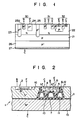
- Figure 1 is a sectional view showing a semiconductor device in which a power transistor section formed from the upper to lower surface of the semiconductor device and an IC section for controlling the transistor section are formed on one chip.
- n-type epitaxial layer 22 is formed on a p-type semiconductor substrate 21.
- Epitaxial layer 22 is divided into a power transistor section and a control IC section.
- Power transistor 30 in the power transistor section comprises n-type base region 25, forming part of epitaxial layer 22, p--type emitter region 24 and n +- type base contact region 25a formed in base region 25, and p-type collector layer 21 and p+- type collector contact layer 26 constituting the semiconductor substrate.
- Collector electrode 27 is formed on the bottom surface of the structure.
- the control IC section comprises active elements (e.g., bipolar or MOS transistors) and passive elements (e.g., resistors, capacitors, and the like) formed in the epitaxial layer.
- active elements e.g., bipolar or MOS transistors
- passive elements e.g., resistors, capacitors, and the like
- the number of elements differs depending on the type of device, but in general, several to several tens of elements are formed.
- p-channel MOS transistor 31 and bipolar transistor 32 are exemplified as active elements.
- P ++- type region 23 isolates the power transistor section from the control IC section and reaches as far as p-type collector layer 21.
- Epitaxial layer 22, in which the control IC section is formed, is thus surrounded by region 23 and collector layer 21. More specifically, a pn junction is formed around the control IC section. Normally, since collector electrode 27 is fixed at a minimum potential in the substrate, the pn junction is reverse-biased during turn-on of the device, thus forming a depletion layer which performs elements isolation.
- a composite semiconductor device comprising:
- the annular groove can be filled with the first insulating layer but need not be completely filled, and the first insulating layer can be formed only on its side walls. In this case, the groove is completely filled with the filling material by a CVD process.
- an insulating material such as Si0 2 , Si 3 N 4 , or the like can be used as the filling material, polycrystalline silicon having substantially the same thermal expansion coefficient as the silicon substrate is preferable.
- a bonding layer is normally formed at a bonding interface between the first and second semiconductor substrates.
- a process for manufacturing a composite semiconductor device comprising the steps of: .
- the surface roughness of the mirror-polished surface is preferably 50 nm (500 A) or less.
- surface roughness is given by a maximum height (Rmax) defined by JIS B-0601 (1982).
- An optical polishing method can be adopted as a mirror polishing method.
- the mirror-polished surface is preferably washed with water, surfactant, organic solvent, acid solution, or the like to remove stain films or contaminants (e.g., fine particles, absorbed ions, organic material, or inorganic material).
- stain films or contaminants e.g., fine particles, absorbed ions, organic material, or inorganic material.
- the mirror-polished surfaces of the first and second semiconductor substrates must be bonded in a clean atmosphere.
- the heating temperature for bonding preferably falls within the range of 1,000 to 1,200°C. High temperatures, at which the first and second semiconductor substrates may fuse together, should be avoided.
- the first functional element is reliably isolated from the second functional element by the deep insulating layer, thus achieving element isolation with a high breakdown voltage.
- the first functional element will not be influenced by heat from the second functional element due to the presence of the space therebetween.
- vertical type power transistor 2 as a second functional element, and an IC, as a first functional element, for controlling transistor 2 are formed in composite silicon substrate 1.
- IC as a first functional element, for controlling transistor 2
- FIG 2 only planar transistor 6 is shown as a component of the control IC.
- Composite silicon substrate 1 is formed by bonding together n--type first silicon substrate 1a a and n +- type second silicon substrate 1 b.
- IC forming portion 4 in which the control IC is formed, is a rectangular plate-like surface layer in first silicon substrate 1a having a thickness of about 20 um.
- Two pillars 5 are formed on the bottom surface of portion 4. The side surfaces of portion 4 are covered with silicon oxide layer 7 and filling material layer 8. Portion 4 is thus isolated from the remaining portion of substrate 1a by layers 7 and 8.
- Space 11 is formed below portion 4 in substrate 1a, and two pillars 5 project downward in space 11 from the bottom surface of portion 4.
- Surfaces of substrates 1a and 1b (including the surfaces of pillars 5) exposed to space 11 are covered with silicon oxide layer 7 and filling material layer 8.
- Silicon oxide layer 10 is sandwiched between pillars 5 and substrate 1b to isolate them from each other. In this way, portion 4 and pillars 5 projecting therefrom are electrically isolated from the remaining portion of substrate 1a and from substrate 1b.
- npn transistor 2 is formed in the remaining portion of substrate 1a.
- the collector contact layer of transistor 2 is formed on a surface opposite the bonding surface of substrate 1 b.
- the composite semiconductor device is prepared as follows.
- Figures 3A to 3F are sectional views showing major steps in the manufacture of the device of the present invention
- Figure 4 is a plan view of substrate 1a after the step in Figure 3A.
- N--type first silicon substrate 1a and n +- type second silicon substrate 1b are prepared.
- One surface of each is mirror-polished to obtain a surface roughness of 50 nm (500 A) or less, thus forming first and second mirror-polished surfaces.
- Substrates 1a and 1b can be degreased if needed. Rectangular recess 11 a having a mesa cross-section and a depth of about 80 ⁇ m is then formed in the first mirror-polished surface of substrate 1a.
- Substrate 1a is patterned to leave two pillars 5 in recess 11 a, as shown in Figure 3A.
- Mesa recess 11a is formed by chemical etching using an oxide film (not shown) as a mask, but can be formed by reactive ion etching (to be referred to as RIE hereinafter) ( Figures 3A and 4).
- the first and second mirror-polished surfaces of substrates 1 a and 1 b are placed in contact with each other in a clean atmosphere so that no foreign substances are present therebetween, and are then heated to 1,200°C to be bonded together. This is performed by a vacuum heating apparatus.
- reference numeral 3 denotes a bonding layer formed at the boundary between substrates 1a and 1b b ( Figure 3B).
- the surface of substrate 1a is lapped to reduce its thickness to 100 pm, so that the thickness of the portion of substrate 1a above recess 11 is reduced to 20 um ( Figure 3C).
- 3-um thick oxide (Si0 2 ) film 13 is formed on the lapped surface of substrate 1a.
- a resist is patterned by a photoetching process method (PEP method), and annular groove 12a is formed in the portion of film 13 corresponding to the peripheral edge portion of recess 11 by RIE.
- Substrate 1a is then etched by RIE using film 13 as a mask to form annular groove 12, which extends to recess 11.
- recess 11 is open to the outer atmosphere through groove 12.
- Portion (the same as the IC forming portion above) 4 of substrate 1a a (thickness: 20 pm) lying on recess 11 is separated from the remaining portion of substrate 1a by groove 12, but can be supported by two pillars 5 so as not to be broken ( Figure 3D).
- Thermal oxidation is then performed via groove 12 in a wet oxygen atmosphere.
- insulating oxide layer 10 is formed between pillars 5 and substrate 1b and until pillars 5 are electrically isolated from bonding layer 3 and substrate 1b adjacent thereto.
- oxide layer 7 is formed on the side walls of grooves 12 and the surfaces of pillars 5.
- Thermal oxidation time is determined by an external oxide layer thickness monitor or test samples.
- insulating layer 10 is formed on the bottom portions of pillars 5. In general, however, the insulating layer is formed on the portion of a pillar which is thinnest and oxidizes most easily ( Figure 3E).
- Groove 12, whose side walls were oxidized, is filled with polycrystalline silicon by a reduced-pressure CVD method, thus air-tightly sealing recess 11.
- Polycrystalline silicon is also deposited on the inner surface of recess 11.
- this deposited portion is not related to the present invention.
- filling material layer 8 formed by filling groove 12 with a filling material, seals recess 11, flattens the exposed surface of substrate 1a, and prevents attachment of foreign substances to recess 11 which cannot be removed later. Since recess 11 is sealed under reduced pressure, internal air will not expand in subsequent heating process, thus preventing damage to the substrate.
- the polycrystalline silicon film, oxide film, and the like attached to the surface of the substrate are removed, and a control IC and power transistor 2 are formed in IC forming portion 4 and in the remaining portion, respectively, of substrate 1a.
- Substrate 1b acts as the collector contact layer of power transistor 2. In this case, the effect of the barrier caused by bonding layer 3 between substrates 1a and 1b on the function of power transistor 2 is negligible.
- the mesa etching step for forming a recess and pillars in substrate 1a is performed in two steps (i.e., deep and shallow etching steps), thus allowing easy control.
- Figure 5A is a sectional view showing substrate 1a after deep mesa etching. More specifically, 80-um rectangular recess 11 a having a mesa cross-section is formed in a first mirror-polished surface of substrate 1a by deep chemical etching. In this case, two pillars 5 are left in the recess region. However, it is difficult to leave bonding surface 13, which will subsequently be bonded to substrate 1b, with high precision by this etching method. Therefore, bonding surface 13 is formed with less precision and a larger area than in Example 1.
- Figure 5B is a sectional view of substrate 1 after shallow mesa etching
- Figure 6 is a plan view thereof.
- a plurality (e.g. 16) of short pillars 5a are formed on surface 13.
- bonding surface 13a of each pillar 5a has an area of 2 tm2.
- Shallow mesa recess 11 b is connected with deep recess 11 a.
- Figure 5C corresponds with Figure 3E in Example 1 and is a sectional view showing the state after annular groove 12 was formed and thermal oxidation was performed.
- insulating oxide layer 10 is formed in the same manner as in Example 1, and pillars 5a are electrically isolated from substrate 1b.
- oxide layer 7 is formed on the side walls of groove 12 and the surfaces of pillars 5 and 5a.
- IC forming portion 4 is dielectrically separated from the remaining portion of substrate 1a and from substrate 1b. The other steps are the same as those in Example 1.
- n +- type impurity be ion-implanted in substrate 1a so as to form an n +- type region on the inner surfaces of recesses 11 a after pillars 5 are formed by selective etching. In this way, the series resistance of the collector can be reduced.
- an isolation breakdown voltage of 1,000 V or higher impossible to obtain with the conventional pn junction separation method, can be realized. Since a large area of an IC forming portion for a control IC is adjacent to a space, heat from a power element (e.g., a power transistor) can be dispersed, and changes in IC characteristics due to heat can be reduced. In addition, isolation capacity and parasitic element effect are reduced when compared with conventional devices, thus providing a stable composite semiconductor device with high reliability.
- a power element e.g., a power transistor
Landscapes
- Engineering & Computer Science (AREA)
- Power Engineering (AREA)
- Physics & Mathematics (AREA)
- Condensed Matter Physics & Semiconductors (AREA)
- General Physics & Mathematics (AREA)
- Computer Hardware Design (AREA)
- Microelectronics & Electronic Packaging (AREA)
- Manufacturing & Machinery (AREA)
- Element Separation (AREA)
- Bipolar Integrated Circuits (AREA)
Description
- The present invention relates to a composite semiconductor device and a process for manufacturing the same and, more particularly, to a composite semiconductor device which consists of a high voltage power element and an integrated circuit formed on one chip and which has a deep element isolation region, and a process for manufactring the same.
- A conventional composite semiconductor device consisting of a high voltage power element and an integrated circuit formed on one chip will be described with reference to Figure 1.
- Figure 1 is a sectional view showing a semiconductor device in which a power transistor section formed from the upper to lower surface of the semiconductor device and an IC section for controlling the transistor section are formed on one chip. Referring to Figure 1, n-type
epitaxial layer 22 is formed on a p-type semiconductor substrate 21.Epitaxial layer 22 is divided into a power transistor section and a control IC section.Power transistor 30 in the power transistor section comprises n-type base region 25, forming part ofepitaxial layer 22, p--type emitter region 24 and n+-type base contact region 25a formed in base region 25, and p-type collector layer 21 and p+- typecollector contact layer 26 constituting the semiconductor substrate.Collector electrode 27 is formed on the bottom surface of the structure. - The control IC section comprises active elements (e.g., bipolar or MOS transistors) and passive elements (e.g., resistors, capacitors, and the like) formed in the epitaxial layer. The number of elements differs depending on the type of device, but in general, several to several tens of elements are formed. In Figure 1, p-
channel MOS transistor 31 andbipolar transistor 32 are exemplified as active elements. - P++-type region 23 isolates the power transistor section from the control IC section and reaches as far as p-
type collector layer 21.Epitaxial layer 22, in which the control IC section is formed, is thus surrounded byregion 23 andcollector layer 21. More specifically, a pn junction is formed around the control IC section. Normally, sincecollector electrode 27 is fixed at a minimum potential in the substrate, the pn junction is reverse-biased during turn-on of the device, thus forming a depletion layer which performs elements isolation. - However, this conventional isolation technique using a pn junction has the following drawbacks.
- (a) Since element isolation is performed using a depletion layer formed when the pn junction is reverse-biased, the breakdown voltage is limited to about 300 V. Therefore, when a 1,000 V class high voltage element (e.g., a power transistor) is to be formed, this isolation technique cannot provide a breakdown voltage high enough to form the element together on one chip with a control IC.
- (b) Even when a 300 V class power element is to be formed, impurity diffusion must be performed to a depth of 40 um or more in order to form a pn junction for isolation, a time consuming process. Since the diffusion width along the lateral direction is increased, the size of the element formation region is reduced.
- (c) A power element normally generates a large amount of heat, thus increasing the temperature of the pellet. A control IC section formed together on one chip with the power element is directly influenced by increases in temperature, and can easily malfunction.
- It is an object of the present invention to provide a composite semiconductor device which is free from the above-mentioned drawbacks of a conventional element isolation technique using a pn junction, which can provide element isolation with a high breakdown voltage, and which has a structure in which elements adjacent to a power transistor are not easily influenced by heat generated by the power transistor.
- According to the present invention, there is provided a composite semiconductor device, comprising:
- a composite substrate consisting of first and second semiconductor substrates, one surface of each of which is mirror-polished, so that the mirror-polished surfaces are bonded together, the first semiconductor substrate having a space adjacent to the bonding interface and an annular groove which communicates with the space from the surface of the first semiconductor substrate opposite the bonding interface, the annular groove being formed in a portion of the first semiconductor substrate corresponding to a peripheral edge portion of the space thereof;
- at least one pillar projecting through the space to the bonding interface from a surface, which is exposed to the space, of a first portion of the first semiconductor substrate which is defined by the space and the annular groove;
- a first insulating layer, formed in the annular groove, for electrically isolating the first portion from a second portion of the first semiconductor substrate adjacent thereto;
- a second insulating layer, formed on the pillar or the bonding interface between the pillar and the second semiconductor substrate, for electrically isolating the first portion from the second semiconductor substrate;
- a first functional element formed in the first portion; and
- a second functional element formed in the second portion.
- The annular groove can be filled with the first insulating layer but need not be completely filled, and the first insulating layer can be formed only on its side walls. In this case, the groove is completely filled with the filling material by a CVD process. Although an insulating material such as Si02, Si3N4, or the like can be used as the filling material, polycrystalline silicon having substantially the same thermal expansion coefficient as the silicon substrate is preferable.
- A bonding layer is normally formed at a bonding interface between the first and second semiconductor substrates.
- Furthermore, according to the present invention, there is provided a process for manufacturing a composite semiconductor device comprising the steps of: .
- mirror-polishing one surface of a first semiconductor substrate;
- mirror-polishing one surface of a second semiconductor substrate;
- selectively etching the mirror-polished surface of the first semiconductor substrate so as to form a recess and in the recess at least one pillar projecting from a bottom portion of the recess to the mirror-polished surface;
- heating the first and second semiconductor substrates after the mirror-polished surfaces thereof have been placed in contact with each other so as to bond them together, thereby forming a composite substrate in which a space including at least one pillar is formed;
- etching a portion of the first semiconductor substrate corresponding to a peripheral edge portion of the space thereof so as to form an annular groove extending to the space and forming a first portion which is defined by the annular groove and the space and is supported by the pillar;
- performing thermal oxidation so as to form an oxide film on a surface, which is exposed to the annular groove and the space, of the composite substrate, whereby the first portion is electrically isolated from a second portion of the first semiconductor substrate, which is adjacent thereto, and the second semiconductor substrate;
- forming .a first functional element in the first portion; and
- forming a second functional element in the second portion.
- In the method of the present invention, the surface roughness of the mirror-polished surface is preferably 50 nm (500 A) or less. Note that "surface roughness" is given by a maximum height (Rmax) defined by JIS B-0601 (1982). An optical polishing method can be adopted as a mirror polishing method.
- After the mirror-polishing step, the mirror-polished surface is preferably washed with water, surfactant, organic solvent, acid solution, or the like to remove stain films or contaminants (e.g., fine particles, absorbed ions, organic material, or inorganic material).
- The mirror-polished surfaces of the first and second semiconductor substrates must be bonded in a clean atmosphere.
- The heating temperature for bonding preferably falls within the range of 1,000 to 1,200°C. High temperatures, at which the first and second semiconductor substrates may fuse together, should be avoided.
- In the composite semiconductor device of the present invention, the first functional element is reliably isolated from the second functional element by the deep insulating layer, thus achieving element isolation with a high breakdown voltage. The first functional element will not be influenced by heat from the second functional element due to the presence of the space therebetween.
- This invention can be more fully understood from the following detailed description when taken in conjunction with the accompanying drawings, in which:
- Figure 1 is a sectional view of a conventional composite semiconductor device;
- Figure 2 is a sectional view of a composite semiconductor device according to an embodiment of the present invention;
- Figures 3A to 3F are sectional views showing steps in the manufacture of the device shown in Figure 2;
- Figure 4 is a plan view of Figure 3A;
- Figures 5A to 5C are sectional views showing steps in the manufacture of a composite semiconductor device according to another embodiment of the present invention; and
- Figure 6 is a plan view of Figure 5A.
- The present invention will now be described by way of examples with reference to the accompanying drawings.
- In the composite semiconductor device shown in Figure 2, vertical
type power transistor 2 as a second functional element, and an IC, as a first functional element, for controllingtransistor 2, are formed in composite silicon substrate 1. In Figure 2, onlyplanar transistor 6 is shown as a component of the control IC. - Composite silicon substrate 1 is formed by bonding together n--type first silicon substrate 1a a and n+-type second silicon substrate 1 b.
IC forming portion 4, in which the control IC is formed, is a rectangular plate-like surface layer in first silicon substrate 1a having a thickness of about 20 um. Twopillars 5 are formed on the bottom surface ofportion 4. The side surfaces ofportion 4 are covered withsilicon oxide layer 7 and fillingmaterial layer 8.Portion 4 is thus isolated from the remaining portion of substrate 1a bylayers -
Space 11 is formed belowportion 4 in substrate 1a, and twopillars 5 project downward inspace 11 from the bottom surface ofportion 4. Surfaces of substrates 1a and 1b (including the surfaces of pillars 5) exposed tospace 11 are covered withsilicon oxide layer 7 and fillingmaterial layer 8.Silicon oxide layer 10 is sandwiched betweenpillars 5 and substrate 1b to isolate them from each other. In this way,portion 4 andpillars 5 projecting therefrom are electrically isolated from the remaining portion of substrate 1a and from substrate 1b. - Vertical
type npn transistor 2 is formed in the remaining portion of substrate 1a. The collector contact layer oftransistor 2 is formed on a surface opposite the bonding surface of substrate 1 b. - The composite semiconductor device is prepared as follows. Figures 3A to 3F are sectional views showing major steps in the manufacture of the device of the present invention, and Figure 4 is a plan view of substrate 1a after the step in Figure 3A. N--type first silicon substrate 1a and n+-type second silicon substrate 1b are prepared. One surface of each is mirror-polished to obtain a surface roughness of 50 nm (500 A) or less, thus forming first and second mirror-polished surfaces. Substrates 1a and 1b can be degreased if needed. Rectangular recess 11 a having a mesa cross-section and a depth of about 80 µm is then formed in the first mirror-polished surface of substrate 1a. Substrate 1a is patterned to leave two
pillars 5 in recess 11 a, as shown in Figure 3A. Mesa recess 11a is formed by chemical etching using an oxide film (not shown) as a mask, but can be formed by reactive ion etching (to be referred to as RIE hereinafter) (Figures 3A and 4). - The first and second mirror-polished surfaces of substrates 1 a and 1 b are placed in contact with each other in a clean atmosphere so that no foreign substances are present therebetween, and are then heated to 1,200°C to be bonded together. This is performed by a vacuum heating apparatus. Note that
reference numeral 3 denotes a bonding layer formed at the boundary between substrates 1a and 1b b (Figure 3B). Next, the surface of substrate 1a is lapped to reduce its thickness to 100 pm, so that the thickness of the portion of substrate 1a aboverecess 11 is reduced to 20 um (Figure 3C). 3-um thick oxide (Si02) film 13 is formed on the lapped surface of substrate 1a. A resist is patterned by a photoetching process method (PEP method), and annular groove 12a is formed in the portion of film 13 corresponding to the peripheral edge portion ofrecess 11 by RIE. Substrate 1a is then etched by RIE using film 13 as a mask to formannular groove 12, which extends to recess 11. Thus,recess 11 is open to the outer atmosphere throughgroove 12. Portion (the same as the IC forming portion above) 4 of substrate 1a a (thickness: 20 pm) lying onrecess 11 is separated from the remaining portion of substrate 1a bygroove 12, but can be supported by twopillars 5 so as not to be broken (Figure 3D). Thermal oxidation is then performed viagroove 12 in a wet oxygen atmosphere. This is continued until insulatingoxide layer 10 is formed betweenpillars 5 and substrate 1b and untilpillars 5 are electrically isolated frombonding layer 3 and substrate 1b adjacent thereto. At the same time,oxide layer 7 is formed on the side walls ofgrooves 12 and the surfaces ofpillars 5. Thermal oxidation time is determined by an external oxide layer thickness monitor or test samples. In this example, insulatinglayer 10 is formed on the bottom portions ofpillars 5. In general, however, the insulating layer is formed on the portion of a pillar which is thinnest and oxidizes most easily (Figure 3E).Groove 12, whose side walls were oxidized, is filled with polycrystalline silicon by a reduced-pressure CVD method, thus air-tightly sealingrecess 11. - Polycrystalline silicon is also deposited on the inner surface of
recess 11. However, this deposited portion is not related to the present invention. In this example, fillingmaterial layer 8, formed by fillinggroove 12 with a filling material, sealsrecess 11, flattens the exposed surface of substrate 1a, and prevents attachment of foreign substances to recess 11 which cannot be removed later. Sincerecess 11 is sealed under reduced pressure, internal air will not expand in subsequent heating process, thus preventing damage to the substrate. - The polycrystalline silicon film, oxide film, and the like attached to the surface of the substrate are removed, and a control IC and
power transistor 2 are formed inIC forming portion 4 and in the remaining portion, respectively, of substrate 1a. Substrate 1b acts as the collector contact layer ofpower transistor 2. In this case, the effect of the barrier caused bybonding layer 3 between substrates 1a and 1b on the function ofpower transistor 2 is negligible. - In this example, the mesa etching step for forming a recess and pillars in substrate 1a is performed in two steps (i.e., deep and shallow etching steps), thus allowing easy control. Figure 5A is a sectional view showing substrate 1a after deep mesa etching. More specifically, 80-um rectangular recess 11 a having a mesa cross-section is formed in a first mirror-polished surface of substrate 1a by deep chemical etching. In this case, two
pillars 5 are left in the recess region. However, it is difficult to leave bonding surface 13, which will subsequently be bonded to substrate 1b, with high precision by this etching method. Therefore, bonding surface 13 is formed with less precision and a larger area than in Example 1. Figure 5B is a sectional view of substrate 1 after shallow mesa etching, and Figure 6 is a plan view thereof. With this etching step, a plurality (e.g. 16) of short pillars 5a are formed on surface 13. For example, bonding surface 13a of each pillar 5a has an area of 2 tm2. Shallow mesa recess 11 b is connected with deep recess 11 a. Figure 5C corresponds with Figure 3E in Example 1 and is a sectional view showing the state afterannular groove 12 was formed and thermal oxidation was performed. With the thermal oxidation step, insulatingoxide layer 10 is formed in the same manner as in Example 1, and pillars 5a are electrically isolated from substrate 1b. At the same time,oxide layer 7 is formed on the side walls ofgroove 12 and the surfaces ofpillars 5 and 5a.IC forming portion 4 is dielectrically separated from the remaining portion of substrate 1a and from substrate 1b. The other steps are the same as those in Example 1. - In Examples 1 and 2, it is preferable that an n+- type impurity be ion-implanted in substrate 1a so as to form an n+-type region on the inner surfaces of recesses 11 a after
pillars 5 are formed by selective etching. In this way, the series resistance of the collector can be reduced. - As shown in Examples 1 and 2, in a composite semiconductor device prepared in accordance with the method of the present invention, an isolation breakdown voltage of 1,000 V or higher, impossible to obtain with the conventional pn junction separation method, can be realized. Since a large area of an IC forming portion for a control IC is adjacent to a space, heat from a power element (e.g., a power transistor) can be dispersed, and changes in IC characteristics due to heat can be reduced. In addition, isolation capacity and parasitic element effect are reduced when compared with conventional devices, thus providing a stable composite semiconductor device with high reliability.
Claims (14)
Applications Claiming Priority (2)
| Application Number | Priority Date | Filing Date | Title |
|---|---|---|---|
| JP60024389A JPS61184843A (en) | 1985-02-13 | 1985-02-13 | Composite semiconductor device and manufacture thereof |
| JP24389/85 | 1985-02-13 |
Publications (3)
| Publication Number | Publication Date |
|---|---|
| EP0191476A2 EP0191476A2 (en) | 1986-08-20 |
| EP0191476A3 EP0191476A3 (en) | 1986-10-22 |
| EP0191476B1 true EP0191476B1 (en) | 1989-11-08 |
Family
ID=12136809
Family Applications (1)
| Application Number | Title | Priority Date | Filing Date |
|---|---|---|---|
| EP86101774A Expired EP0191476B1 (en) | 1985-02-13 | 1986-02-12 | Composite semiconductor device and process for manufacturing the same |
Country Status (4)
| Country | Link |
|---|---|
| US (1) | US4710794A (en) |
| EP (1) | EP0191476B1 (en) |
| JP (1) | JPS61184843A (en) |
| DE (1) | DE3666901D1 (en) |
Families Citing this family (50)
| Publication number | Priority date | Publication date | Assignee | Title |
|---|---|---|---|---|
| US4949162A (en) * | 1987-06-05 | 1990-08-14 | Hitachi, Ltd. | Semiconductor integrated circuit with dummy pedestals |
| JP2586422B2 (en) * | 1987-10-20 | 1997-02-26 | 日本電装株式会社 | Method of manufacturing dielectric integrated composite integrated circuit device |
| JPH01179342A (en) * | 1988-01-05 | 1989-07-17 | Toshiba Corp | Composite semiconductor crystal |
| JP2788269B2 (en) * | 1988-02-08 | 1998-08-20 | 株式会社東芝 | Semiconductor device and manufacturing method thereof |
| JP2685244B2 (en) * | 1988-09-30 | 1997-12-03 | 株式会社日本自動車部品総合研究所 | Method for manufacturing semiconductor device |
| JPH0656865B2 (en) * | 1988-10-13 | 1994-07-27 | 株式会社東芝 | Adhesive substrate for high voltage devices |
| US5416354A (en) * | 1989-01-06 | 1995-05-16 | Unitrode Corporation | Inverted epitaxial process semiconductor devices |
| US5164218A (en) * | 1989-05-12 | 1992-11-17 | Nippon Soken, Inc. | Semiconductor device and a method for producing the same |
| US5212109A (en) * | 1989-05-24 | 1993-05-18 | Nissan Motor Co., Ltd. | Method for forming PN junction isolation regions by forming buried regions of doped polycrystalline or amorphous semiconductor |
| JP2567472B2 (en) * | 1989-05-24 | 1996-12-25 | 日産自動車株式会社 | Semiconductor device |
| US5264720A (en) * | 1989-09-22 | 1993-11-23 | Nippondenso Co., Ltd. | High withstanding voltage transistor |
| JPH0821619B2 (en) * | 1989-10-13 | 1996-03-04 | 株式会社東芝 | Semiconductor device |
| DD290077A5 (en) * | 1989-12-15 | 1991-05-16 | Adw Der Ddr,De | METHOD OF BONDING SEMICONDUCTOR SUBSTRATES |
| JPH03283636A (en) * | 1990-03-30 | 1991-12-13 | Nippon Soken Inc | Manufacture of semiconductor substrate |
| EP0543361B1 (en) * | 1991-11-20 | 2002-02-27 | Canon Kabushiki Kaisha | Method of manufacturing a semiconductor device |
| DE4204004A1 (en) * | 1992-02-12 | 1993-08-19 | Daimler Benz Ag | METHOD FOR PRODUCING A SEMICONDUCTOR STRUCTURE WITH VERTICAL AND LATERAL SEMICONDUCTOR COMPONENTS AND SEMICONDUCTOR STRUCTURE PRODUCED BY THE METHOD |
| US5389569A (en) * | 1992-03-03 | 1995-02-14 | Motorola, Inc. | Vertical and lateral isolation for a semiconductor device |
| DE4233773C2 (en) * | 1992-10-07 | 1996-09-19 | Daimler Benz Ag | Semiconductor structure for semiconductor devices with high breakdown voltage |
| US5413962A (en) * | 1994-07-15 | 1995-05-09 | United Microelectronics Corporation | Multi-level conductor process in VLSI fabrication utilizing an air bridge |
| US5796883A (en) * | 1995-09-04 | 1998-08-18 | Nec Corporation | Optical integrated circuit and method for fabricating the same |
| US5949144A (en) * | 1996-05-20 | 1999-09-07 | Harris Corporation | Pre-bond cavity air bridge |
| DE19840421C2 (en) * | 1998-06-22 | 2000-05-31 | Fraunhofer Ges Forschung | Process for the production of thin substrate layers and a suitable substrate arrangement |
| EP1043775B1 (en) * | 1999-04-06 | 2006-06-14 | STMicroelectronics S.r.l. | Power integrated circuit with vertical current flow and related manufacturing process |
| EP1043769A1 (en) * | 1999-04-07 | 2000-10-11 | STMicroelectronics S.r.l. | Process for manufacturing a semiconductor material wafer comprising single-crystal regions separated by insulating material regions, in particular for manufacturing intergrated power devices, and wafer thus obtained |
| JP3957038B2 (en) * | 2000-11-28 | 2007-08-08 | シャープ株式会社 | Semiconductor substrate and manufacturing method thereof |
| FR2819630B1 (en) * | 2001-01-12 | 2003-08-15 | St Microelectronics Sa | SEMICONDUCTOR DEVICE WITH INSULATED ZONE AND MANUFACTURING METHOD THEREOF |
| US20030037874A1 (en) * | 2001-07-26 | 2003-02-27 | Massachusetts Institute Of Technology | Semiconductor substrate bonding by mass transport growth fusion |
| DE10144343A1 (en) * | 2001-09-10 | 2003-03-27 | Perkinelmer Optoelectronics | Sensor for contactless measurement of a temperature |
| JP4556158B2 (en) | 2002-10-22 | 2010-10-06 | 株式会社Sumco | Method for manufacturing bonded SOI substrate and semiconductor device |
| JP4020195B2 (en) | 2002-12-19 | 2007-12-12 | 三菱電機株式会社 | Method for manufacturing dielectric isolation type semiconductor device |
| US20070057289A1 (en) | 2004-01-10 | 2007-03-15 | Davies Robert B | Power semiconductor device and method therefor |
| FR2875947B1 (en) | 2004-09-30 | 2007-09-07 | Tracit Technologies | NOVEL STRUCTURE FOR MICROELECTRONICS AND MICROSYSTEMS AND METHOD OF MAKING SAME |
| FR2876220B1 (en) * | 2004-10-06 | 2007-09-28 | Commissariat Energie Atomique | METHOD FOR PRODUCING MIXED STACKED STRUCTURES, VARIOUS INSULATING AREAS AND / OR LOCALIZED VERTICAL ELECTRICAL CONDUCTION ZONES. |
| US8530963B2 (en) * | 2005-01-06 | 2013-09-10 | Estivation Properties Llc | Power semiconductor device and method therefor |
| EP1969622B1 (en) * | 2005-12-21 | 2018-11-14 | Kromek Limited | Semiconductor device and method of manufacture thereof |
| GB2433648A (en) * | 2005-12-21 | 2007-06-27 | Durham Scient Crystals Ltd | Radiation detector formed by deposition of bulk semiconductor crystal layers |
| FR2897982B1 (en) | 2006-02-27 | 2008-07-11 | Tracit Technologies Sa | METHOD FOR MANUFACTURING PARTIALLY-LIKE STRUCTURES, COMPRISING AREAS CONNECTING A SURFACE LAYER AND A SUBSTRATE |
| JP2006310836A (en) * | 2006-04-05 | 2006-11-09 | Hvvi Semiconductors Inc | Power semiconductor device and its method |
| JP2006310838A (en) * | 2006-04-05 | 2006-11-09 | Hvvi Semiconductors Inc | Power semiconductor device and its method |
| DE102007001523A1 (en) * | 2007-01-10 | 2008-07-17 | Infineon Technologies Ag | Semiconductor circuit arrangement, has semiconductor material region provided with two semiconductor circuit parts, and void structure with hollow cavity, which is arranged between semiconductor circuit parts |
| US9666703B2 (en) | 2014-12-17 | 2017-05-30 | Great Wall Semiconductor Corporation | Semiconductor devices with cavities |
| US10461152B2 (en) | 2017-07-10 | 2019-10-29 | Globalfoundries Inc. | Radio frequency switches with air gap structures |
| WO2019083729A1 (en) * | 2017-10-23 | 2019-05-02 | Trustees Of Boston University | Enhanced thermal transport across interfaces |
| US10446643B2 (en) | 2018-01-22 | 2019-10-15 | Globalfoundries Inc. | Sealed cavity structures with a planar surface |
| US11056382B2 (en) * | 2018-03-19 | 2021-07-06 | Globalfoundries U.S. Inc. | Cavity formation within and under semiconductor devices |
| US11410872B2 (en) * | 2018-11-30 | 2022-08-09 | Globalfoundries U.S. Inc. | Oxidized cavity structures within and under semiconductor devices |
| US10923577B2 (en) | 2019-01-07 | 2021-02-16 | Globalfoundries U.S. Inc. | Cavity structures under shallow trench isolation regions |
| US11127816B2 (en) | 2020-02-14 | 2021-09-21 | Globalfoundries U.S. Inc. | Heterojunction bipolar transistors with one or more sealed airgap |
| US11764258B2 (en) * | 2020-12-01 | 2023-09-19 | Globalfoundries U.S. Inc. | Airgap isolation structures |
| US11881506B2 (en) | 2021-07-27 | 2024-01-23 | Globalfoundries U.S. Inc. | Gate structures with air gap isolation features |
Family Cites Families (10)
| Publication number | Priority date | Publication date | Assignee | Title |
|---|---|---|---|---|
| US3412296A (en) * | 1965-10-19 | 1968-11-19 | Sprague Electric Co | Monolithic structure with threeregion or field effect complementary transistors |
| JPS5423388A (en) * | 1977-07-22 | 1979-02-21 | Hitachi Ltd | Semiconductor integrated-circuit device and its manufacture |
| JPS5440084A (en) * | 1977-09-05 | 1979-03-28 | Fujitsu Ltd | Semiconductor device and manufacture thereof |
| DE2926741C2 (en) * | 1979-07-03 | 1982-09-09 | Licentia Patent-Verwaltungs-Gmbh, 6000 Frankfurt | Field effect transistor and process for its manufacture |
| US4411060A (en) * | 1981-07-06 | 1983-10-25 | Western Electric Co., Inc. | Method of manufacturing dielectrically-isolated single-crystal semiconductor substrates |
| US4661832A (en) * | 1982-06-30 | 1987-04-28 | International Business Machines Corporation | Total dielectric isolation for integrated circuits |
| US4502913A (en) * | 1982-06-30 | 1985-03-05 | International Business Machines Corporation | Total dielectric isolation for integrated circuits |
| US4467521A (en) * | 1983-08-15 | 1984-08-28 | Sperry Corporation | Selective epitaxial growth of gallium arsenide with selective orientation |
| JPS60113455A (en) * | 1983-11-24 | 1985-06-19 | Hitachi Ltd | Semiconductor ic device |
| EP0161740B1 (en) * | 1984-05-09 | 1991-06-12 | Kabushiki Kaisha Toshiba | Method of manufacturing semiconductor substrate |
-
1985
- 1985-02-13 JP JP60024389A patent/JPS61184843A/en active Granted
-
1986
- 1986-02-12 EP EP86101774A patent/EP0191476B1/en not_active Expired
- 1986-02-12 DE DE8686101774T patent/DE3666901D1/en not_active Expired
- 1986-02-12 US US06/828,536 patent/US4710794A/en not_active Expired - Lifetime
Also Published As
| Publication number | Publication date |
|---|---|
| JPS61184843A (en) | 1986-08-18 |
| DE3666901D1 (en) | 1989-12-14 |
| EP0191476A3 (en) | 1986-10-22 |
| JPH0473621B2 (en) | 1992-11-24 |
| EP0191476A2 (en) | 1986-08-20 |
| US4710794A (en) | 1987-12-01 |
Similar Documents
| Publication | Publication Date | Title |
|---|---|---|
| EP0191476B1 (en) | Composite semiconductor device and process for manufacturing the same | |
| JP2788269B2 (en) | Semiconductor device and manufacturing method thereof | |
| US5627399A (en) | Semiconductor device | |
| US5004705A (en) | Inverted epitaxial process | |
| EP0176747B1 (en) | Silicon semiconductor substrate with an insulating layer embedded therein and method for forming the same | |
| EP0615286B1 (en) | Semiconductor device provided with isolation region | |
| EP0323856B1 (en) | Substrate structure for composite semiconductor device | |
| EP0653785B1 (en) | Di-electric isolated type semiconductor device | |
| US5476809A (en) | Semiconductor device and method of manufacturing the same | |
| JP3014012B2 (en) | Method for manufacturing semiconductor device | |
| US3416224A (en) | Integrated semiconductor devices and fabrication methods therefor | |
| JP3818673B2 (en) | Semiconductor device | |
| US3772577A (en) | Guard ring mesa construction for low and high voltage npn and pnp transistors and diodes and method of making same | |
| US4372030A (en) | Method for producing a semiconductor device | |
| US5406113A (en) | Bipolar transistor having a buried collector layer | |
| JP2979554B2 (en) | Method for manufacturing semiconductor device | |
| EP0789403B1 (en) | Zener zap diode and method of manufacturing the same | |
| US5763931A (en) | Semiconductor device with SOI structure and fabrication method thereof | |
| JP3148766B2 (en) | Semiconductor device | |
| JPH0629376A (en) | Integrated circuit device | |
| JPS61172346A (en) | Semiconductor integrated circuit device | |
| JPH09129763A (en) | Semiconductor integrated circuit | |
| JPH0547914A (en) | Dielectric isolation substrate and its manufacture | |
| JPH05243502A (en) | Integrated circuit | |
| JPH0258367A (en) | Semiconductor device |
Legal Events
| Date | Code | Title | Description |
|---|---|---|---|
| PUAI | Public reference made under article 153(3) epc to a published international application that has entered the european phase |
Free format text: ORIGINAL CODE: 0009012 |
|
| 17P | Request for examination filed |
Effective date: 19860212 |
|
| AK | Designated contracting states |
Kind code of ref document: A2 Designated state(s): DE FR GB NL |
|
| PUAL | Search report despatched |
Free format text: ORIGINAL CODE: 0009013 |
|
| AK | Designated contracting states |
Kind code of ref document: A3 Designated state(s): DE FR GB NL |
|
| 17Q | First examination report despatched |
Effective date: 19890222 |
|
| GRAA | (expected) grant |
Free format text: ORIGINAL CODE: 0009210 |
|
| AK | Designated contracting states |
Kind code of ref document: B1 Designated state(s): DE FR GB NL |
|
| REF | Corresponds to: |
Ref document number: 3666901 Country of ref document: DE Date of ref document: 19891214 |
|
| ET | Fr: translation filed | ||
| PLBE | No opposition filed within time limit |
Free format text: ORIGINAL CODE: 0009261 |
|
| STAA | Information on the status of an ep patent application or granted ep patent |
Free format text: STATUS: NO OPPOSITION FILED WITHIN TIME LIMIT |
|
| 26N | No opposition filed | ||
| PGFP | Annual fee paid to national office [announced via postgrant information from national office to epo] |
Ref country code: GB Payment date: 19970203 Year of fee payment: 12 |
|
| PGFP | Annual fee paid to national office [announced via postgrant information from national office to epo] |
Ref country code: FR Payment date: 19970211 Year of fee payment: 12 |
|
| PGFP | Annual fee paid to national office [announced via postgrant information from national office to epo] |
Ref country code: DE Payment date: 19970221 Year of fee payment: 12 |
|
| PG25 | Lapsed in a contracting state [announced via postgrant information from national office to epo] |
Ref country code: GB Free format text: LAPSE BECAUSE OF NON-PAYMENT OF DUE FEES Effective date: 19980212 |
|
| PG25 | Lapsed in a contracting state [announced via postgrant information from national office to epo] |
Ref country code: FR Free format text: THE PATENT HAS BEEN ANNULLED BY A DECISION OF A NATIONAL AUTHORITY Effective date: 19980228 |
|
| GBPC | Gb: european patent ceased through non-payment of renewal fee |
Effective date: 19980212 |
|
| PG25 | Lapsed in a contracting state [announced via postgrant information from national office to epo] |
Ref country code: DE Free format text: LAPSE BECAUSE OF NON-PAYMENT OF DUE FEES Effective date: 19981103 |
|
| REG | Reference to a national code |
Ref country code: FR Ref legal event code: ST |
|
| PGFP | Annual fee paid to national office [announced via postgrant information from national office to epo] |
Ref country code: NL Payment date: 20050203 Year of fee payment: 20 |
|
| PG25 | Lapsed in a contracting state [announced via postgrant information from national office to epo] |
Ref country code: NL Free format text: LAPSE BECAUSE OF EXPIRATION OF PROTECTION Effective date: 20060212 |
|
| NLV7 | Nl: ceased due to reaching the maximum lifetime of a patent |
Effective date: 20060212 |