EP0187601A2 - Trockenes Ätzverfahren für eine Siliziumnitridschicht - Google Patents
Trockenes Ätzverfahren für eine Siliziumnitridschicht Download PDFInfo
- Publication number
- EP0187601A2 EP0187601A2 EP85402634A EP85402634A EP0187601A2 EP 0187601 A2 EP0187601 A2 EP 0187601A2 EP 85402634 A EP85402634 A EP 85402634A EP 85402634 A EP85402634 A EP 85402634A EP 0187601 A2 EP0187601 A2 EP 0187601A2
- Authority
- EP
- European Patent Office
- Prior art keywords
- layer
- silicon
- silicon nitride
- nitride layer
- etching
- Prior art date
- Legal status (The legal status is an assumption and is not a legal conclusion. Google has not performed a legal analysis and makes no representation as to the accuracy of the status listed.)
- Granted
Links
- 229910052581 Si3N4 Inorganic materials 0.000 title claims abstract description 62
- HQVNEWCFYHHQES-UHFFFAOYSA-N silicon nitride Chemical compound N12[Si]34N5[Si]62N3[Si]51N64 HQVNEWCFYHHQES-UHFFFAOYSA-N 0.000 title claims abstract description 62
- 238000000034 method Methods 0.000 title claims abstract description 38
- 238000001312 dry etching Methods 0.000 title claims abstract description 19
- VYPSYNLAJGMNEJ-UHFFFAOYSA-N Silicium dioxide Chemical compound O=[Si]=O VYPSYNLAJGMNEJ-UHFFFAOYSA-N 0.000 claims abstract description 69
- 238000005530 etching Methods 0.000 claims abstract description 35
- XUIMIQQOPSSXEZ-UHFFFAOYSA-N Silicon Chemical compound [Si] XUIMIQQOPSSXEZ-UHFFFAOYSA-N 0.000 claims abstract description 29
- 229910052710 silicon Inorganic materials 0.000 claims abstract description 29
- 239000010703 silicon Substances 0.000 claims abstract description 29
- 239000000377 silicon dioxide Substances 0.000 claims abstract description 25
- 229910018503 SF6 Inorganic materials 0.000 claims abstract description 16
- 235000012239 silicon dioxide Nutrition 0.000 claims abstract description 12
- 230000001590 oxidative effect Effects 0.000 claims abstract description 6
- SFZCNBIFKDRMGX-UHFFFAOYSA-N sulfur hexafluoride Chemical compound FS(F)(F)(F)(F)F SFZCNBIFKDRMGX-UHFFFAOYSA-N 0.000 claims abstract description 6
- 229960000909 sulfur hexafluoride Drugs 0.000 claims abstract description 6
- 238000000059 patterning Methods 0.000 claims abstract description 4
- RWRIWBAIICGTTQ-UHFFFAOYSA-N difluoromethane Chemical group FCF RWRIWBAIICGTTQ-UHFFFAOYSA-N 0.000 claims description 14
- NBVXSUQYWXRMNV-UHFFFAOYSA-N fluoromethane Chemical compound FC NBVXSUQYWXRMNV-UHFFFAOYSA-N 0.000 claims description 10
- 238000001020 plasma etching Methods 0.000 claims description 6
- 239000007789 gas Substances 0.000 description 18
- 229910052681 coesite Inorganic materials 0.000 description 16
- 229910052906 cristobalite Inorganic materials 0.000 description 16
- 229910052682 stishovite Inorganic materials 0.000 description 16
- 229910052905 tridymite Inorganic materials 0.000 description 16
- WRQGPGZATPOHHX-UHFFFAOYSA-N ethyl 2-oxohexanoate Chemical compound CCCCC(=O)C(=O)OCC WRQGPGZATPOHHX-UHFFFAOYSA-N 0.000 description 10
- 230000003647 oxidation Effects 0.000 description 9
- 238000007254 oxidation reaction Methods 0.000 description 9
- 210000003323 beak Anatomy 0.000 description 8
- TXEYQDLBPFQVAA-UHFFFAOYSA-N tetrafluoromethane Chemical compound FC(F)(F)F TXEYQDLBPFQVAA-UHFFFAOYSA-N 0.000 description 5
- 238000006243 chemical reaction Methods 0.000 description 4
- 230000008878 coupling Effects 0.000 description 3
- 238000010168 coupling process Methods 0.000 description 3
- 238000005859 coupling reaction Methods 0.000 description 3
- QKCGXXHCELUCKW-UHFFFAOYSA-N n-[4-[4-(dinaphthalen-2-ylamino)phenyl]phenyl]-n-naphthalen-2-ylnaphthalen-2-amine Chemical compound C1=CC=CC2=CC(N(C=3C=CC(=CC=3)C=3C=CC(=CC=3)N(C=3C=C4C=CC=CC4=CC=3)C=3C=C4C=CC=CC4=CC=3)C3=CC4=CC=CC=C4C=C3)=CC=C21 QKCGXXHCELUCKW-UHFFFAOYSA-N 0.000 description 3
- CURLTUGMZLYLDI-UHFFFAOYSA-N Carbon dioxide Chemical compound O=C=O CURLTUGMZLYLDI-UHFFFAOYSA-N 0.000 description 2
- ZAMOUSCENKQFHK-UHFFFAOYSA-N Chlorine atom Chemical compound [Cl] ZAMOUSCENKQFHK-UHFFFAOYSA-N 0.000 description 2
- VGGSQFUCUMXWEO-UHFFFAOYSA-N Ethene Chemical compound C=C VGGSQFUCUMXWEO-UHFFFAOYSA-N 0.000 description 2
- 229910052782 aluminium Inorganic materials 0.000 description 2
- XAGFODPZIPBFFR-UHFFFAOYSA-N aluminium Chemical compound [Al] XAGFODPZIPBFFR-UHFFFAOYSA-N 0.000 description 2
- 239000000203 mixture Substances 0.000 description 2
- 239000004065 semiconductor Substances 0.000 description 2
- OKTJSMMVPCPJKN-UHFFFAOYSA-N Carbon Chemical compound [C] OKTJSMMVPCPJKN-UHFFFAOYSA-N 0.000 description 1
- 239000005977 Ethylene Substances 0.000 description 1
- PXGOKWXKJXAPGV-UHFFFAOYSA-N Fluorine Chemical compound FF PXGOKWXKJXAPGV-UHFFFAOYSA-N 0.000 description 1
- XPDWGBQVDMORPB-UHFFFAOYSA-N Fluoroform Chemical compound FC(F)F XPDWGBQVDMORPB-UHFFFAOYSA-N 0.000 description 1
- 230000015572 biosynthetic process Effects 0.000 description 1
- 229910052799 carbon Inorganic materials 0.000 description 1
- 229910002092 carbon dioxide Inorganic materials 0.000 description 1
- 239000001569 carbon dioxide Substances 0.000 description 1
- 239000000460 chlorine Substances 0.000 description 1
- 229910052801 chlorine Inorganic materials 0.000 description 1
- 229910021419 crystalline silicon Inorganic materials 0.000 description 1
- 230000003247 decreasing effect Effects 0.000 description 1
- 238000000280 densification Methods 0.000 description 1
- 238000002474 experimental method Methods 0.000 description 1
- 229910052731 fluorine Inorganic materials 0.000 description 1
- 239000011737 fluorine Substances 0.000 description 1
- 229910052751 metal Inorganic materials 0.000 description 1
- 239000002184 metal Substances 0.000 description 1
- 229920003986 novolac Polymers 0.000 description 1
- 229920002120 photoresistant polymer Polymers 0.000 description 1
- 229910021420 polycrystalline silicon Inorganic materials 0.000 description 1
- 239000010453 quartz Substances 0.000 description 1
- 239000012495 reaction gas Substances 0.000 description 1
- 238000004544 sputter deposition Methods 0.000 description 1
Images


Classifications
-
- H—ELECTRICITY
- H01—ELECTRIC ELEMENTS
- H01L—SEMICONDUCTOR DEVICES NOT COVERED BY CLASS H10
- H01L21/00—Processes or apparatus adapted for the manufacture or treatment of semiconductor or solid state devices or of parts thereof
- H01L21/02—Manufacture or treatment of semiconductor devices or of parts thereof
- H01L21/04—Manufacture or treatment of semiconductor devices or of parts thereof the devices having potential barriers, e.g. a PN junction, depletion layer or carrier concentration layer
- H01L21/06—Manufacture or treatment of semiconductor devices or of parts thereof the devices having potential barriers, e.g. a PN junction, depletion layer or carrier concentration layer the devices having semiconductor bodies comprising selenium or tellurium in uncombined form other than as impurities in semiconductor bodies of other materials
- H01L21/14—Treatment of the complete device, e.g. by electroforming to form a barrier
- H01L21/145—Ageing
-
- H—ELECTRICITY
- H01—ELECTRIC ELEMENTS
- H01L—SEMICONDUCTOR DEVICES NOT COVERED BY CLASS H10
- H01L21/00—Processes or apparatus adapted for the manufacture or treatment of semiconductor or solid state devices or of parts thereof
- H01L21/02—Manufacture or treatment of semiconductor devices or of parts thereof
- H01L21/04—Manufacture or treatment of semiconductor devices or of parts thereof the devices having potential barriers, e.g. a PN junction, depletion layer or carrier concentration layer
- H01L21/18—Manufacture or treatment of semiconductor devices or of parts thereof the devices having potential barriers, e.g. a PN junction, depletion layer or carrier concentration layer the devices having semiconductor bodies comprising elements of Group IV of the Periodic Table or AIIIBV compounds with or without impurities, e.g. doping materials
- H01L21/30—Treatment of semiconductor bodies using processes or apparatus not provided for in groups H01L21/20 - H01L21/26
- H01L21/31—Treatment of semiconductor bodies using processes or apparatus not provided for in groups H01L21/20 - H01L21/26 to form insulating layers thereon, e.g. for masking or by using photolithographic techniques; After treatment of these layers; Selection of materials for these layers
- H01L21/32—Treatment of semiconductor bodies using processes or apparatus not provided for in groups H01L21/20 - H01L21/26 to form insulating layers thereon, e.g. for masking or by using photolithographic techniques; After treatment of these layers; Selection of materials for these layers using masks
-
- H—ELECTRICITY
- H01—ELECTRIC ELEMENTS
- H01L—SEMICONDUCTOR DEVICES NOT COVERED BY CLASS H10
- H01L21/00—Processes or apparatus adapted for the manufacture or treatment of semiconductor or solid state devices or of parts thereof
- H01L21/02—Manufacture or treatment of semiconductor devices or of parts thereof
- H01L21/04—Manufacture or treatment of semiconductor devices or of parts thereof the devices having potential barriers, e.g. a PN junction, depletion layer or carrier concentration layer
- H01L21/18—Manufacture or treatment of semiconductor devices or of parts thereof the devices having potential barriers, e.g. a PN junction, depletion layer or carrier concentration layer the devices having semiconductor bodies comprising elements of Group IV of the Periodic Table or AIIIBV compounds with or without impurities, e.g. doping materials
- H01L21/30—Treatment of semiconductor bodies using processes or apparatus not provided for in groups H01L21/20 - H01L21/26
- H01L21/302—Treatment of semiconductor bodies using processes or apparatus not provided for in groups H01L21/20 - H01L21/26 to change their surface-physical characteristics or shape, e.g. etching, polishing, cutting
-
- H—ELECTRICITY
- H01—ELECTRIC ELEMENTS
- H01L—SEMICONDUCTOR DEVICES NOT COVERED BY CLASS H10
- H01L21/00—Processes or apparatus adapted for the manufacture or treatment of semiconductor or solid state devices or of parts thereof
- H01L21/02—Manufacture or treatment of semiconductor devices or of parts thereof
- H01L21/04—Manufacture or treatment of semiconductor devices or of parts thereof the devices having potential barriers, e.g. a PN junction, depletion layer or carrier concentration layer
- H01L21/18—Manufacture or treatment of semiconductor devices or of parts thereof the devices having potential barriers, e.g. a PN junction, depletion layer or carrier concentration layer the devices having semiconductor bodies comprising elements of Group IV of the Periodic Table or AIIIBV compounds with or without impurities, e.g. doping materials
- H01L21/30—Treatment of semiconductor bodies using processes or apparatus not provided for in groups H01L21/20 - H01L21/26
- H01L21/31—Treatment of semiconductor bodies using processes or apparatus not provided for in groups H01L21/20 - H01L21/26 to form insulating layers thereon, e.g. for masking or by using photolithographic techniques; After treatment of these layers; Selection of materials for these layers
- H01L21/3105—After-treatment
- H01L21/311—Etching the insulating layers by chemical or physical means
- H01L21/31105—Etching inorganic layers
- H01L21/31111—Etching inorganic layers by chemical means
- H01L21/31116—Etching inorganic layers by chemical means by dry-etching
-
- H—ELECTRICITY
- H01—ELECTRIC ELEMENTS
- H01L—SEMICONDUCTOR DEVICES NOT COVERED BY CLASS H10
- H01L21/00—Processes or apparatus adapted for the manufacture or treatment of semiconductor or solid state devices or of parts thereof
- H01L21/70—Manufacture or treatment of devices consisting of a plurality of solid state components formed in or on a common substrate or of parts thereof; Manufacture of integrated circuit devices or of parts thereof
- H01L21/71—Manufacture of specific parts of devices defined in group H01L21/70
- H01L21/76—Making of isolation regions between components
- H01L21/762—Dielectric regions, e.g. EPIC dielectric isolation, LOCOS; Trench refilling techniques, SOI technology, use of channel stoppers
- H01L21/76202—Dielectric regions, e.g. EPIC dielectric isolation, LOCOS; Trench refilling techniques, SOI technology, use of channel stoppers using a local oxidation of silicon, e.g. LOCOS, SWAMI, SILO
Definitions
- the present invention relates to a process for etching a silicon nitride layer. Move specifically, it relates to a process for dry etching a silicon nitride layer on a silicon dioxide layer, useful in a so-called "local oxidation of silicon” (LOCOS) process.
- LOC local oxidation of silicon
- a silicon nitride (Si 3 N 4 ) layer is used as a mask for locally oxidizing a semiconductor bulk, such as a silicon bulk.
- a silicon bulk such as a silicon bulk.
- LOC silicon nitride
- the overall surface of a silicon bulk is first oxidized to a thin thickness, e.g., 50 nm.
- an Si 3 N 4 layer of, e.g., 100 nm thickness is formed on the oxidized surface of the silicon bulk.
- the Si 3 N 4 layer is patterned with a mask of a patterned resist layer formed on the si 3 N 4 layer, the resist layer is removed, then the silicon bulk is locally oxidized by using the patterned Si 3 N 4 layer as a mask.
- An etching gas comprising fluoromethane (fleon), particularly tetrafluoromethane (CF 4 ), and oxigen (O 2 ) is typically used for dry etching an Si 3 N 4 layer in the LOCOS process, which gas needs the above mentioned combination of thicknesses of the SiO 2 and Si 3 N 4 layers of, e.g., 50 nm and 100 nm, respectively, since the above etching gas has a ratio of etching rate of Si 3 N 4 to SiO 2 of about 2 to 3 at the highest.
- fluoromethane fluoromethane
- CF 4 tetrafluoromethane
- O 2 oxigen
- the Si0 2 layer may be over etched during the patterning or etching of an Si 3 N 4 layer on the Si0 2 layer, which causes nonuniform oxidation of the silicon bulk existing under the SiO 2 layer.
- etching gases for example, a mixed gas of sulfur hexafluoride (SF 6 ) and chlorine (C1 2 ) for etching silicon (Japanese Unexamined Patent Publication (Kokai) No. 58-7829); a gas of SF 6 , nitrogen trifluoride (NF 3 ), fluorine (F 2 ), or C1 2 for etching silicon (Japanese Unexamined Patent Publication (Kokai) No. 59-214226); a gas of NF 3 for etching Si 3 N 4 (Japanese Unexamined Patent Publication (Kokai) No.
- the main object of the present invention is to provide an effective dry etching process for etching Si 3 N 4 .
- a further object of the present invention is to provide a dry etching process having a high ratio of etching rate of Si 3 N 4 /Si0 2 , useful for the LOCOS process.
- a still further object of the present invention is to reduce the size of "bird beaks" formed in the LOCOS process in order to densify semiconductor IC devices.
- a process for dry etching an Si 3 N 4 layer with an etching gas comprising SF 6 is based on a finding that SF 6 has a high effectivity of etching Si 3 N 4 and a high selectivity of etching Si 3 N 4 in relation to SiO 2 or a photoresist.
- the etching gas optionally further comprises, e.g., fluoromethane such as CH 3 F, CH 2 F 2 , CHF 3 , and CF 4 .
- fluoromethane such as CH 3 F, CH 2 F 2 , CHF 3 , and CF 4 .
- a combination of SF 6 and CH 2 F 2 is preferred.
- anode coupling reactive ion etching is preferable in a process for dry etching an Si 3 N 4 layer on an Si0 2 layer with an etching gas comprising SF 6 and optionally CH 2 F 2 since it allows a higher etching rate ratio of Si 3 N 4 /SiO 2 , although other types of dry etching, for example, cathode coupling type, reactive ion etching, and downflow type plasma etching, may have some advantages in a process according to the present invention.
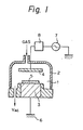
- Figure 1 illustrates an anode coupling type dry etching apparatus.
- a reaction chamber 1 defined by a quartz tube 2
- An upper side electrode 3 is made of aluminum (Al) and anodized on its surface
- a lower side electrode 4 is made of aluminum on which a wafer 5 to be treated is placed.
- the lower side electrode 4 is connected to the ground 6, and the upper side electrode 3 is connected to a radio frequency (RF) source 7 of 13.56 MHz.
- RF radio frequency
- a matching network 8 is inserted between the upper side electrode 3 and the RF source 7.
- the reaction chamber 1 is evacuated by a vacuum pump (not shown).
- a silicon (Si) bulk or wafer 11 was prepared and a surface of the silicon bulk 11 was oxidized to form an Si0 2 layer 12 of 30 nm thickness.
- An Si 3 N 4 layer 13 was deposited onto the SiO 2 layer 12 by sputtering, etc. The thickness of the Si 3 N 4 layer 13 was 100 nm in this case, but could have also been made 150 nm.
- a resist layer 14 was coated on the Si 3 N 4 layer 13 and patterned to leave a square or rectangular shape having a size L of 2.5 um.
- a dry etching apparatus as in Fig. 1, the wafer 1 was placed on the lower side electrode 4.
- a radio frequency of 13.56 MHz was applied between the two electrodes 3 and 4 at a power of about 125 Watts.
- a portion of the Si 3 N 4 layer 13 which was not covered with the patterned resist layer 14, was selectively etched or removed.
- the resist layer 14 was then removed.
- a patterned Si 3 N 4 layer 13 was obtained on the SiO 2 layer 12; the patterned Si 3 N 4 layer 13 having a square or rectangular shape, as shown in Fig. 2B.
- oxidation was carried out in which the patterned Si 3 N 4 layer 13 was used as a mask to locally oxidize the silicon bulk 11, that is, a portion of the silicon bulk 11 above which no Si 3 N 4 layer exists was oxidized to form a thick Si0 2 layer 14 or a locally oxidized silicon.
- "bird beaks" b were formed but had the width B of only 0.2 ⁇ m to 0.3 ⁇ m which was reduced from the width of the "bird beaks" in the prior art.
- the thickness of the Si0 2 layer had to be 50 nm if the Si 3 N 4 layer had a thickness of 100 nm. This resulted in a width of the "bird beaks" of 0.3 ⁇ m to 0.4 ⁇ m after patterning the Si 3 N 4 layer and oxidizing the silicon bulk under the SiO 2 layer using the Si 3 N 4 layer as a mask.
- the thickness of an Si 3 N 4 layer was made 150 nm while maintaining the thickness of an SiO 2 layer at 30 nm. Successful selective etching of the Si 3 N 4 layer could be done, that is, the Si0 2 layer was not overetched, resulting in excellent local oxidation of a silicon bulk under the Si0 2 layer.
- the flow rate of CH 2 F 2 was varied with the other conditions being fixed.
- the fixed conditions of the test were vacuum of 0.25 Torr, RF power of 125 Watts, flow rate of the SF 6 of 50 SCCM, and temperature of 25°C.
- the etching rates of an Si 3 N 4 layer, an SiO 2 layer, and a resist layer were determined.
- the obtained etching rates and the selectivities of Si 3 N 4 to SiO 2 and resist or ratios of the etching rate of Si 3 N 4 to Si0 2 and resist, respectively, are summarized in the graphs in Figs. 3 and 4.
- a selectivity of etching of Si 3 N 4 to Si0 2 of more than 3, particularly, more than 4 was obtained in a process according to the present invention while at the highest only a selectivity of 2 to 3 could be obtained in a process in the prior art.
- a relatively high selectivity of etching of Si 3 N 4 /resist was obtained and is also preferable.
- a mixing ratio by volume or mole of CH 2 F 2 :CF 6 of up to 35:100, more preferably 8 - 24:100, particularly 20:100, is preferably used in a process according to the present invention. This fact was ascertained in another test in which the flow-rate of CF 6 is varied with the other conditions being fixed.
- a third test in which the degree of vacuum in a reaction chamber was varied and the other conditions were fixed was carried out.
Landscapes
- Engineering & Computer Science (AREA)
- Microelectronics & Electronic Packaging (AREA)
- Condensed Matter Physics & Semiconductors (AREA)
- General Physics & Mathematics (AREA)
- Manufacturing & Machinery (AREA)
- Computer Hardware Design (AREA)
- Physics & Mathematics (AREA)
- Power Engineering (AREA)
- Chemical & Material Sciences (AREA)
- Chemical Kinetics & Catalysis (AREA)
- General Chemical & Material Sciences (AREA)
- Inorganic Chemistry (AREA)
- Health & Medical Sciences (AREA)
- Gerontology & Geriatric Medicine (AREA)
- Drying Of Semiconductors (AREA)
Applications Claiming Priority (2)
| Application Number | Priority Date | Filing Date | Title |
|---|---|---|---|
| JP280138/84 | 1984-12-29 | ||
| JP59280138A JPS61158143A (ja) | 1984-12-29 | 1984-12-29 | 窒化シリコン膜のエッチング方法 |
Publications (3)
| Publication Number | Publication Date |
|---|---|
| EP0187601A2 true EP0187601A2 (de) | 1986-07-16 |
| EP0187601A3 EP0187601A3 (en) | 1988-03-16 |
| EP0187601B1 EP0187601B1 (de) | 1991-03-13 |
Family
ID=17620865
Family Applications (1)
| Application Number | Title | Priority Date | Filing Date |
|---|---|---|---|
| EP85402634A Expired - Lifetime EP0187601B1 (de) | 1984-12-29 | 1985-12-26 | Trockenes Ätzverfahren für eine Siliziumnitridschicht |
Country Status (4)
| Country | Link |
|---|---|
| EP (1) | EP0187601B1 (de) |
| JP (1) | JPS61158143A (de) |
| KR (1) | KR900006020B1 (de) |
| DE (1) | DE3582146D1 (de) |
Cited By (1)
| Publication number | Priority date | Publication date | Assignee | Title |
|---|---|---|---|---|
| WO2003012829A1 (de) * | 2001-07-24 | 2003-02-13 | Osram Opto Semiconductors Gmbh | Verfahren zur herstellung einer linse |
Families Citing this family (1)
| Publication number | Priority date | Publication date | Assignee | Title |
|---|---|---|---|---|
| JP2720962B2 (ja) * | 1985-10-29 | 1998-03-04 | ソニー株式会社 | エツチングガス及びこれを用いたエツチング方法 |
Citations (2)
| Publication number | Priority date | Publication date | Assignee | Title |
|---|---|---|---|---|
| EP0109706A1 (de) * | 1982-11-16 | 1984-05-30 | Koninklijke Philips Electronics N.V. | Verfahren zur Herstellung einer Halbleiteranordnung unter Verwendung eines Plasmaätzverfahrens |
| DE3420347A1 (de) * | 1983-06-01 | 1984-12-06 | Hitachi, Ltd., Tokio/Tokyo | Gas und verfahren zum selektiven aetzen von siliciumnitrid |
Family Cites Families (1)
| Publication number | Priority date | Publication date | Assignee | Title |
|---|---|---|---|---|
| JPH0612765B2 (ja) * | 1983-06-01 | 1994-02-16 | 株式会社日立製作所 | エ ッ チ ン グ 方 法 |
-
1984
- 1984-12-29 JP JP59280138A patent/JPS61158143A/ja active Granted
-
1985
- 1985-12-26 DE DE8585402634T patent/DE3582146D1/de not_active Expired - Fee Related
- 1985-12-26 EP EP85402634A patent/EP0187601B1/de not_active Expired - Lifetime
- 1985-12-28 KR KR1019850010029A patent/KR900006020B1/ko not_active IP Right Cessation
Patent Citations (2)
| Publication number | Priority date | Publication date | Assignee | Title |
|---|---|---|---|---|
| EP0109706A1 (de) * | 1982-11-16 | 1984-05-30 | Koninklijke Philips Electronics N.V. | Verfahren zur Herstellung einer Halbleiteranordnung unter Verwendung eines Plasmaätzverfahrens |
| DE3420347A1 (de) * | 1983-06-01 | 1984-12-06 | Hitachi, Ltd., Tokio/Tokyo | Gas und verfahren zum selektiven aetzen von siliciumnitrid |
Non-Patent Citations (1)
| Title |
|---|
| IEEE TRANSACTIONS ON ELECTRON DEVICES, vol. ED-28, no. 11, November 1981, pages 1332-1337, IEEE, New York, US; W. BEINVOGL et al.: "Plasma etching of polysilicon and Si3N4 in SF6 with some impact on MOS device characteristics" * |
Cited By (1)
| Publication number | Priority date | Publication date | Assignee | Title |
|---|---|---|---|---|
| WO2003012829A1 (de) * | 2001-07-24 | 2003-02-13 | Osram Opto Semiconductors Gmbh | Verfahren zur herstellung einer linse |
Also Published As
| Publication number | Publication date |
|---|---|
| EP0187601B1 (de) | 1991-03-13 |
| DE3582146D1 (de) | 1991-04-18 |
| KR900006020B1 (ko) | 1990-08-20 |
| JPS61158143A (ja) | 1986-07-17 |
| JPH0426539B2 (de) | 1992-05-07 |
| KR860005431A (ko) | 1986-07-23 |
| EP0187601A3 (en) | 1988-03-16 |
Similar Documents
| Publication | Publication Date | Title |
|---|---|---|
| US7273566B2 (en) | Gas compositions | |
| US7541270B2 (en) | Methods for forming openings in doped silicon dioxide | |
| US6015760A (en) | Method for enhancing oxide to nitride selectivity through the use of independent heat control | |
| US8093155B2 (en) | Method of controlling striations and CD loss in contact oxide etch | |
| US7166535B2 (en) | Plasma etching of silicon carbide | |
| US7153779B2 (en) | Method to eliminate striations and surface roughness caused by dry etch | |
| US5843226A (en) | Etch process for single crystal silicon | |
| US4717447A (en) | Method of manufacturing a semiconductor device by means of plasma etching | |
| EP0256311A2 (de) | RIE-Verfahren um Isolationsrillen mit senkrechten Flanken in Silizium und Polycid zu ätzen | |
| US20060186087A1 (en) | Etchant and method of use | |
| US20070077724A1 (en) | Etching methods and apparatus and substrate assemblies produced therewith | |
| KR20010042983A (ko) | 고 종횡비 개구를 형성하는 방법 | |
| US4678539A (en) | Dry-etching method | |
| KR100311487B1 (ko) | 산화막식각방법 | |
| US6117788A (en) | Semiconductor etching methods | |
| US6372634B1 (en) | Plasma etch chemistry and method of improving etch control | |
| US5180466A (en) | Process for dry etching a silicon nitride layer | |
| US6069087A (en) | Highly selective dry etching process | |
| EP0187601B1 (de) | Trockenes Ätzverfahren für eine Siliziumnitridschicht | |
| US6653237B2 (en) | High resist-selectivity etch for silicon trench etch applications | |
| JPH0859215A (ja) | 窒化物エッチングプロセス |
Legal Events
| Date | Code | Title | Description |
|---|---|---|---|
| PUAI | Public reference made under article 153(3) epc to a published international application that has entered the european phase |
Free format text: ORIGINAL CODE: 0009012 |
|
| AK | Designated contracting states |
Kind code of ref document: A2 Designated state(s): DE FR GB |
|
| PUAL | Search report despatched |
Free format text: ORIGINAL CODE: 0009013 |
|
| AK | Designated contracting states |
Kind code of ref document: A3 Designated state(s): DE FR GB |
|
| 17P | Request for examination filed |
Effective date: 19880428 |
|
| 17Q | First examination report despatched |
Effective date: 19900420 |
|
| GRAA | (expected) grant |
Free format text: ORIGINAL CODE: 0009210 |
|
| AK | Designated contracting states |
Kind code of ref document: B1 Designated state(s): DE FR GB |
|
| REF | Corresponds to: |
Ref document number: 3582146 Country of ref document: DE Date of ref document: 19910418 |
|
| ET | Fr: translation filed | ||
| PLBE | No opposition filed within time limit |
Free format text: ORIGINAL CODE: 0009261 |
|
| STAA | Information on the status of an ep patent application or granted ep patent |
Free format text: STATUS: NO OPPOSITION FILED WITHIN TIME LIMIT |
|
| 26N | No opposition filed | ||
| PGFP | Annual fee paid to national office [announced via postgrant information from national office to epo] |
Ref country code: DE Payment date: 19930226 Year of fee payment: 8 |
|
| PG25 | Lapsed in a contracting state [announced via postgrant information from national office to epo] |
Ref country code: DE Effective date: 19940901 |
|
| PGFP | Annual fee paid to national office [announced via postgrant information from national office to epo] |
Ref country code: FR Payment date: 19951212 Year of fee payment: 11 |
|
| PGFP | Annual fee paid to national office [announced via postgrant information from national office to epo] |
Ref country code: GB Payment date: 19951218 Year of fee payment: 11 |
|
| PG25 | Lapsed in a contracting state [announced via postgrant information from national office to epo] |
Ref country code: GB Effective date: 19961226 |
|
| GBPC | Gb: european patent ceased through non-payment of renewal fee |
Effective date: 19961226 |
|
| PG25 | Lapsed in a contracting state [announced via postgrant information from national office to epo] |
Ref country code: FR Effective date: 19970829 |
|
| REG | Reference to a national code |
Ref country code: FR Ref legal event code: ST |