EP0185263B1 - Appareil pour la représentation de deux objets disposés dans des plans d'objet différents - Google Patents
Appareil pour la représentation de deux objets disposés dans des plans d'objet différents Download PDFInfo
- Publication number
- EP0185263B1 EP0185263B1 EP85115482A EP85115482A EP0185263B1 EP 0185263 B1 EP0185263 B1 EP 0185263B1 EP 85115482 A EP85115482 A EP 85115482A EP 85115482 A EP85115482 A EP 85115482A EP 0185263 B1 EP0185263 B1 EP 0185263B1
- Authority
- EP
- European Patent Office
- Prior art keywords
- housing
- housing section
- adjustable
- optical
- mask
- Prior art date
- Legal status (The legal status is an assumption and is not a legal conclusion. Google has not performed a legal analysis and makes no representation as to the accuracy of the status listed.)
- Expired
Links
Images

Classifications
-
- G—PHYSICS
- G03—PHOTOGRAPHY; CINEMATOGRAPHY; ANALOGOUS TECHNIQUES USING WAVES OTHER THAN OPTICAL WAVES; ELECTROGRAPHY; HOLOGRAPHY
- G03F—PHOTOMECHANICAL PRODUCTION OF TEXTURED OR PATTERNED SURFACES, e.g. FOR PRINTING, FOR PROCESSING OF SEMICONDUCTOR DEVICES; MATERIALS THEREFOR; ORIGINALS THEREFOR; APPARATUS SPECIALLY ADAPTED THEREFOR
- G03F9/00—Registration or positioning of originals, masks, frames, photographic sheets or textured or patterned surfaces, e.g. automatically
- G03F9/70—Registration or positioning of originals, masks, frames, photographic sheets or textured or patterned surfaces, e.g. automatically for microlithography
- G03F9/7069—Alignment mark illumination, e.g. darkfield, dual focus
-
- G—PHYSICS
- G03—PHOTOGRAPHY; CINEMATOGRAPHY; ANALOGOUS TECHNIQUES USING WAVES OTHER THAN OPTICAL WAVES; ELECTROGRAPHY; HOLOGRAPHY
- G03F—PHOTOMECHANICAL PRODUCTION OF TEXTURED OR PATTERNED SURFACES, e.g. FOR PRINTING, FOR PROCESSING OF SEMICONDUCTOR DEVICES; MATERIALS THEREFOR; ORIGINALS THEREFOR; APPARATUS SPECIALLY ADAPTED THEREFOR
- G03F9/00—Registration or positioning of originals, masks, frames, photographic sheets or textured or patterned surfaces, e.g. automatically
- G03F9/70—Registration or positioning of originals, masks, frames, photographic sheets or textured or patterned surfaces, e.g. automatically for microlithography
- G03F9/7003—Alignment type or strategy, e.g. leveling, global alignment
- G03F9/7023—Aligning or positioning in direction perpendicular to substrate surface
- G03F9/7026—Focusing
Definitions
- the invention relates to a device for optically imaging two objects arranged in different object planes onto an optical sensor, in which at least one objective can be adjusted relative to the object planes with the aid of an actuator.
- the finest structures are transferred to semiconductor wafers with the aid of masks, whereby a highly precise adjustment from mask to wafer is required.
- the transfer of structures in the submicrometer range by means of X-ray lithography requires an adjustment from mask to disc with accuracies in the range below 0.1 p.m.
- a method for automatic mask adjustment in which the adjustment of successive masks is carried out in each case with adjustment structures running orthogonally to one another on the semiconductor wafer coated with a photoresist and on the mask.
- the alignment structure of the semiconductor wafer is already produced in the first structuring process on the surface of the semiconductor wafer, for example by etching, so that the alignment structures present on the corresponding mask can be aligned with respect to this first alignment structure in all subsequent structuring processes.
- the adjustment structures on the mask and disk are then scanned in directions parallel to their edges with the aid of an optical sensor, whereupon the intensity of the image signals generated by the optoelectronic scanning is integrated line by line or line by line and the resulting analog integral values are converted into digital gray levels and saved.
- the position of the center axes of the adjustment structures can then be detected, whereupon the semiconductor wafer and mask for adjustment are shifted and rotated relative to one another in accordance with the offset of the center lines.
- the proximity distance between the mask and the semiconductor wafer limits the detection and adjustment accuracy that can be achieved. If, for example, the focal plane is placed between the mask plane and the disk plane in a microscopic image, the adjustment structures of both planes are only blurred on the optical sensor. The evaluation of the widened optoelectronic edge signals for the determination of the relative position of the mask and the semiconductor wafer is then not clear, i.e. the accuracy of the position detection is limited.
- a two-level optical system in which either the mask plane or the wafer plane can be imaged sharply on the optical sensor by two different optical path lengths in the beam path of the imaging optical system .
- Fluctuations in the proximity distance between the mask and the semiconductor wafer, unevenness in the surface of the banknotes and different thicknesses of the photoresist on the surface of the wafer also impair the sharpness of the image of the edge transitions in the individual object planes.
- the limits of opto-electronic gray-scale image processing can only be reached if the alignment structures of the mask and semiconductor wafer are clearly imaged onto the optical sensor during image acquisition.
- the invention has for its object to provide a device for the optical imaging of two objects arranged in different object planes on an optical sensor, in which at least one objective with the help of an actuator relative to the object planes is absolutely shift-free and with a very high positioning repeatability for focusing can be adjusted.
- the actuator is supported on a stationary housing and engages a housing section that is adjustable relative to the object planes and at least supports the lens, that the stationary housing and the adjustable housing section are formed in one piece and that the adjustable housing section Housing section is connected to the stationary housing via spring joints arranged symmetrically to the optical axis, which are formed by elastically deformable weak points of the housing.
- the invention is based on the knowledge that that an absolutely shift-free adjustment of the lens with the required high positioning repeatability can only be achieved if the lens is adjusted together with the housing section in or on which it is rigidly attached.
- An important prerequisite is that the spring joints required for the adjustability of this housing section are formed by elastically deformable weak points in the housing, ie that the adjustable housing section must be connected in one piece to the other stationary housing via the spring joints. The same properties of all spring joints can only be guaranteed by such a one-piece formation of the spring joints from the housing.
- the actuating drive engaging the adjustable housing section is supported on the stationary housing, which is done in a simple manner by means of a rib of the stationary housing which projects into the adjustable housing section.
- At least four spring joints arranged in pairs on opposite sides of the adjustable housing section are provided. With such a paired arrangement of at least four spring joints, the required shift-free adjustment of the adjustable housing section can be implemented particularly easily.
- each spring joint is formed by two weak points arranged at a distance from one another, each weak point being formed by grooves made in the wall of the housing on opposite sides. Due to the possibility of inserting the grooves into the wall of the housing with the highest precision, the spring lengths and the effective cross-sections of the spring joints can be specified with correspondingly high precision, which leads to a high reproducibility of the force-displacement behavior of the adjustable housing section.
- the grooves preferably have a semicircular cross section, since this cross-sectional shape avoids an undesirable concentration of local bending stresses.
- separating slots are made between the adjustable housing section and the rest of the housing, each of which extends between two spring joints. The introduction of such separating slots enables the adjustable housing section to be moved in a particularly simple manner.
- a piezo actuator is provided as the actuator.
- an adjustment path of 1/100 ⁇ m can be assigned to an adjustment voltage of 1 V, for example.
- an objective with an infinite image width is provided, which is followed by a tube lens carried by the stationary housing.
- the advantage of using a lens with an infinite image width lies in the parallel beam path between the lens and the tube lens.
- the overall magnification of the device is not changed by adjusting the lens.
- the actuator acting centrally between the optical axes on the adjustable housing section carrying both lenses. Since the mask adjustment requires both translational and rotary position movements, the division into two fields of view arranged at a distance from one another brings considerable advantages.
- the actuator can then be arranged in a simple manner between the optical axes of the two lenses so that a particularly compact design of the entire device results.
- FIG. 1 shows a semiconductor wafer Hs to which the finest structures in the submicrometer range are to be transferred by means of X-ray lithography.
- the masks M required for these structure transfers must be adjusted with accuracies in the range below 0.1! Jm with respect to the semiconductor wafer Hs, such a precise adjustment no longer being possible visually but only automatically.
- mutually orthogonal adjustment structures are provided, which are applied to the mask M and the semiconductor wafer Hs at two spaced locations and, in the case shown, are designed as adjustment crosses.
- the alignment crosses applied to the semiconductor wafer Hs are designated JkS1 and JkS2, while the associated alignment crosses on the mask M are designated JkM1 and JkM2.
- the alignment crosses JkS1 and JkS2 are arranged in a first object plane Oel, while the alignment crosses JkM1 and JkM2 are arranged in a second object plane Oe2.
- the distance, referred to as proximity distance Pa, between the object planes Oel and Oe2 can be subject to fluctuations, whereby these fluctuations, for example, range between 30 ⁇ m and 50 ⁇ m.
- the alignment crosses JkS1 and JkM1 are scanned in directions running parallel to their edges with the aid of an optical sensor, which in the case shown is designed as a TV camera TVK1 with electronic image rotation through 90 °.
- the image signals Bs1 generated by the optoelectronic scanning are then supplied on the one hand to a TV monitor TVM1 and on the other hand to an image processing device Bv.
- the optical crosses JkS1 and JkM1 are imaged on the TV camera TVK1 via an objective Ob1 with an infinite image width, a tube lens TIi, an eyepiece Ok1 and a deflection device Ue1 shown as a deflection mirror, the optical components listed above being arranged one after the other in the beam path.
- the alignment crosses JkS2 and JkM2 are scanned in directions running parallel to their edges with the aid of an optical sensor, which in the case shown is designed as a TV camera TVK2 with electronic image rotation through 90 °.
- the image signals Bs2 generated by the optoelectronic scanning are then supplied on the one hand to a TV monitor TVM2 and on the other hand to the already mentioned image processing device Bv.
- the optical crosses JkS2 and JkM2 are imaged on the TV camera TVK2 via an objective Ob2 with an infinite image width, a tube lens T12, an eyepiece Ok2 and a deflection device Ue2 shown as a deflection mirror, the optical components listed above being arranged one after the other in the beam path.
- the intensity of the image signals Bs1 and Bs2 generated by the optoelectronic scanning is integrated line by line or line by line in the image processing device Bv, whereupon the resulting analog integral values are converted into digital gray levels and stored.
- the position of the central axes of the alignment crosses JkS1 and JkM1 or JkS2 and JkM2 can then be detected in a position detection device Le, whereupon the semiconductor wafer Hs and mask M are shifted relative to one another in accordance with the determined offset of the center lines and be twisted.
- the adjustment variables ⁇ x, ⁇ y and ⁇ formed by the position detection device Le as control signals are fed to a piezo adjustment Pv, which is only schematically illustrated and which causes the displacement in two mutually perpendicular directions in accordance with the arrows x and y and the rotation in accordance with the arrow ⁇ .
- the arrow Pf is intended to indicate that the individual piezo actuators of the piezo adjustment Pv are driven by a high voltage of, for example, 1000 V.
- the proximity distance Pa between the mask M and the semiconductor wafer Hs limits the detection and adjustment accuracy that can be achieved, unless additional measures for image acquisition succeed, the adjustment structures of the mask M and semiconductor wafer Hs are clearly sharp on the TV Mapping cameras TVK1 and TVK2. This is to be achieved by continuously refocusing the image contents of mask M and semiconductor wafer Hs.
- a piezocontrolled, shift-free adjustment of the objectives Ob1 and Ob2 is provided for the continuous adjustment of the sharpness of the alignment structures on the mask M and the semiconductor wafer Hs in the two spatially separated fields of view, the adjustability of the objectives Ob1 and Ob2 relative to the object planes Oe1 and Oe2 in Figure 1 is shown only schematically by double arrows Pf1 and Pf2.
- An auto focus can then be realized by software evaluation of the integrated edge signals of mask M and semiconductor wafer Hs. The focus level results from the maximization of local correlation functions at the edge transition.
- an actuator provided for the object adjustment can then be automatically adjusted to the optimal focus level of mask M or semiconductor wafer Hs.
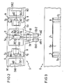
- FIGS. 2 and 3 show the design of a device for optically imaging the alignment structures of the mask and semiconductor wafer on an optical sensor in the front view and in the top view.
- the design shown here is based on the basic mode of operation shown in FIG. 1, with the exception of a few minor modifications.
- the housing of the device is mirror-symmetrical to a plane of symmetry Se, this symmetry taking into account the division into the two spatially separate fields of view.
- the upper, horizontally oriented wall W1 of the housing G is connected to the lower, parallel wall W2 via vertical transverse webs Qs1 and Qs2, which are equidistant from the plane of symmetry Se.
- an adjustable housing section generally designated Ga, which is connected to the remaining stationary housing G by four spring joints Fg arranged in pairs on opposite sides.
- this adjustable housing section Ga relative to the remaining stationary housing G is made possible by two separating slots Ts light, which are introduced into the upper wall W1 or the lower wall W2 and extend between the corresponding spring joints Fg.
- Each of the four spring joints Fg is formed by two weak points arranged at a distance from one another, each of these weak points being formed by two grooves N, which are made on opposite sides in the upper wall W1 and the lower wall W2 of the housing G and have a semicircular cross section.
- the adjustable housing section Ga thus remains connected in one piece with the remaining stationary housing G via the four spring joints Fg.
- the adjustable housing section Ga takes up only part of the depth of the housing G.
- stiffening webs Vs1 and Vs2, which are strong extend between the upper wall W1 and the lower wall W2, which in turn are equidistant from the plane of symmetry Se.
- a housing extension Gf which is trapezoidal in shape and internally hollow is formed on the underside of the adjustable housing section Ga, which carries on its underside a first lens barrel Obt1 and a lens barrel Obt2 equally distant from the plane of symmetry.
- the objective Ob1 shown in FIG. 1 or a corresponding lens system is located in the lens barrel Obt1, while the objective Ob2 shown in FIG. 1 or a corresponding lens system is located in the lens barrel Obt2.
- the tube lenses T11 and T12 shown in FIG. 1 are arranged in a common tube lens holder TH, which protrudes into the cavity of the housing extension Gf and is anchored in an identical housing part set of the remaining stationary housing G which is separated by the separating slot Ts.
- the deflection devices Ue1 and Ue2 are not between the eyepieces Ok1 or Ok2 and the TV cameras TVK1 or TVK2, but between the tube lenses T11 or T12 and Eyepieces Ok1 and Ok2 arranged.
- the optical axes oA1 and oA2 initially assigned to the two fields of view and initially running vertically follow the deflection devices Ue1 or Ue2 a horizontal course.
- the eyepieces or lens systems corresponding to the eyepieces Ok1 and Ok2 are then arranged after the deflection devices Ue1 and Ue2 and are held in an eyepiece tube Oct1 and an eyepiece tube Oct2.
- the eyepiece tube Okt1 is fastened in an eyepiece tube holder OH1 arranged between the crosspiece Qs1 and the stiffening strap Vs1 and anchored in the stationary housing G, while the eyepiece tube Okt2 is correspondingly arranged in a housing that is arranged between the crosspiece Qs2 and the mounting strap Vs2 and in the stationary housing G anchored eyepiece tube holder OH2 is attached.
- the TV cameras TVK1 and TVK2 are then arranged after the crossbars Qs1 and Qs2, which are fixed to the stationary housing G, but with respect to the optical axes oA1 and oA2 are adjustably connected.
- the shift-free adjustment of the lenses Ob1 and Ob2 (cf. Fig. 1) in the vertical direction of the optical axes oA1 and oA2 to the optimum focus level is carried out with the aid of an actuator Sa designed as a piezo actuator, which engages and acts on the adjustable housing section Ga the stationary housing G is supported.
- the actuator Sa is arranged in the adjustable housing section Ga exactly between the deflection devices Ue1 and Ue2 and is supported on a rib R of the remaining stationary housing G which projects into the adjustable housing section Ga and is very rigid.
- the actuator Sa is, for example, firmly screwed to the rib R, while its movable actuator Sg engages the lower wall W2 of the adjustable housing section Ga and causes an elastic, shift-free deflection of the adjustable housing section Ga and thus also of the lens barrel Obt1 and the lens barrel Obt2 can.
- the lighting arrangement has been omitted in FIG. 1 and in FIGS. 2 and 3.
- the semiconductor wafer Hs and mask M are illuminated in the manner of microscope illumination, in particular according to the Koehler illumination principle, in which the object is illuminated by parallel beams.
- the light is introduced into the device via light guides in order to avoid the development of heat and a corresponding thermal distortion within the device.
- the adjustment of the lenses Ob1 and Ob2 (see FIG. 1) shown in FIGS. 2 and 3 via the adjustable housing section Ga enables an absolutely play-free adjustment with a repeatability of positioning of ⁇ 0.01 ⁇ m with a statistical certainty of 95%.
- the device shown enables the relative position of mask M and semiconductor wafer Hs to be determined with extremely low measurement uncertainties of 0.01 p.m or ⁇ 1 s.
- the adjustable housing section Ga In the device shown in FIGS. 2 and 3, only the objectives Ob1 and Ob2 (cf. FIG. 1) are adjusted with the adjustable housing section Ga. However, it can also be expedient to use the adjustable housing section Ga to adjust all the optical components of the device, including the TV cameras TVK1 and TVKS. In this case, the adjustment of the entire facility becomes easier because the The direction of movement of the lenses Ob1 and Ob2 (cf. FIG. 1) does not have to run exactly parallel to the optical axis oA1 or oA2.
Claims (9)
Applications Claiming Priority (2)
| Application Number | Priority Date | Filing Date | Title |
|---|---|---|---|
| DE3446584 | 1984-12-20 | ||
| DE3446584 | 1984-12-20 |
Publications (2)
| Publication Number | Publication Date |
|---|---|
| EP0185263A1 EP0185263A1 (fr) | 1986-06-25 |
| EP0185263B1 true EP0185263B1 (fr) | 1988-07-27 |
Family
ID=6253369
Family Applications (1)
| Application Number | Title | Priority Date | Filing Date |
|---|---|---|---|
| EP85115482A Expired EP0185263B1 (fr) | 1984-12-20 | 1985-12-05 | Appareil pour la représentation de deux objets disposés dans des plans d'objet différents |
Country Status (4)
| Country | Link |
|---|---|
| US (1) | US4703185A (fr) |
| EP (1) | EP0185263B1 (fr) |
| JP (1) | JP2528790B2 (fr) |
| DE (1) | DE3564042D1 (fr) |
Families Citing this family (2)
| Publication number | Priority date | Publication date | Assignee | Title |
|---|---|---|---|---|
| US5086477A (en) * | 1990-08-07 | 1992-02-04 | Northwest Technology Corp. | Automated system for extracting design and layout information from an integrated circuit |
| US5204739A (en) * | 1992-02-07 | 1993-04-20 | Karl Suss America, Inc. | Proximity mask alignment using a stored video image |
Family Cites Families (9)
| Publication number | Priority date | Publication date | Assignee | Title |
|---|---|---|---|---|
| CH461149A (de) * | 1967-05-09 | 1968-08-15 | Conradi G Ag | Einrichtung an einer Zeichenmaschine oder einem Koordinatographen zur mindestens angenähert fehlerfreien Auftragung von Punkten, Linien und Symbolen auf eine zur Führungsebene des Arbeitswagens nicht parallele und/oder nicht plane photographische Schicht |
| FR2371716A1 (fr) * | 1976-11-19 | 1978-06-16 | Thomson Csf | Appareil photorepeteur de masques |
| EP0005462B1 (fr) * | 1978-05-22 | 1983-06-08 | Siemens Aktiengesellschaft | Procédé pour positionner deux objets à ajuster l'un sur l'autre |
| JPS57187435U (fr) * | 1981-05-22 | 1982-11-27 | ||
| JPS57118207A (en) * | 1981-07-24 | 1982-07-23 | Minolta Camera Co Ltd | Automatic focus adjuster |
| US4580900A (en) * | 1982-04-02 | 1986-04-08 | Eaton Corporation | Auto focus alignment and measurement system and method |
| US4615621A (en) * | 1982-04-02 | 1986-10-07 | Eaton Corporation | Auto-focus alignment and measurement system and method |
| JPS5965943A (ja) * | 1982-10-06 | 1984-04-14 | Alps Electric Co Ltd | 対物レンズ駆動装置 |
| JPS60223122A (ja) * | 1984-04-19 | 1985-11-07 | Canon Inc | 投影露光装置 |
-
1985
- 1985-11-15 US US06/798,411 patent/US4703185A/en not_active Expired - Fee Related
- 1985-12-05 DE DE8585115482T patent/DE3564042D1/de not_active Expired
- 1985-12-05 EP EP85115482A patent/EP0185263B1/fr not_active Expired
- 1985-12-13 JP JP60280870A patent/JP2528790B2/ja not_active Expired - Lifetime
Also Published As
| Publication number | Publication date |
|---|---|
| JPS61153656A (ja) | 1986-07-12 |
| DE3564042D1 (en) | 1988-09-01 |
| EP0185263A1 (fr) | 1986-06-25 |
| US4703185A (en) | 1987-10-27 |
| JP2528790B2 (ja) | 1996-08-28 |
Similar Documents
| Publication | Publication Date | Title |
|---|---|---|
| EP1618426B1 (fr) | Procede et dispositif pour determiner la position du point focal lors de l'obtention d'une image d'un echantillon | |
| EP1393116B1 (fr) | Dispositif de mise au point automatique pour un appareil optique | |
| EP0689700B1 (fr) | Procede d'acquisition de codes a barres | |
| DE10257766A1 (de) | Verfahren zur Einstellung einer gewünschten optischen Eigenschaft eines Projektionsobjektivs sowie mikrolithografische Projektionsbelichtungsanlage | |
| DE3342719C2 (de) | Positionierungseinrichung in einem Projektionsbelichter | |
| DE4131737A1 (de) | Autofokus-anordnung fuer ein stereomikroskop | |
| EP1116932A2 (fr) | Appareil de mesure et méthode pour mesurer des structures sur un substrat | |
| DE10204367B4 (de) | Autofokusmodul für mikroskopbasierte Systeme und Autofokusverfahren für ein mikroskopbasiertes System | |
| DE112019000783T5 (de) | Autofokusvorrichtung und optische Apparatur und Mikroskop mit derselben | |
| DE3910048C2 (fr) | ||
| EP0226893A1 (fr) | Procédé de haute précision de mesure pour structures bidimensionnelles ainsi que masque de référence pour l'utilisation de ce procédé | |
| DE3915642A1 (de) | Ausricht- und belichtungsvorrichtung | |
| EP2764327B1 (fr) | Détermination de la déformation d'un substrat | |
| DE102014107044A1 (de) | Verbessertes Autofokusverfahren für ein Koordinatenmessgerät | |
| EP0185263B1 (fr) | Appareil pour la représentation de deux objets disposés dans des plans d'objet différents | |
| EP0135673A2 (fr) | Procédé et dispositif pour déterminer une coordonnée sur la surface d'un corps solide | |
| DE2458868C3 (de) | Anordnung zur Messung des Fokussierungszustandes in optischen Systemen, insbesondere in photographischen Kameras | |
| EP1538472A1 (fr) | Appareil de formation d'images avec réseau de microlentilles pour l'imagerie stabilisée d'un objet sur un détecteur | |
| DE102022204539A1 (de) | Verfahren zum Justieren einer Kamera | |
| WO2005052695A1 (fr) | Alignement direct dans des dispositifs d'alignement de masque | |
| DE4216724C2 (de) | Vorrichtung zum Erfassen der Scharfeinstellung | |
| EP1179748B1 (fr) | Méthodes combinant le balayage et la visualisation pour une vérification de masque lithographiques | |
| DE102019217629A1 (de) | Verfahren zur Ausrichtung eines Interferometers und Projektionsbelichtungsanlage für die Halbleitertechnik | |
| DE3326346A1 (de) | Optische vorrichtung zur aufrechterhaltung der pupillenabbildung | |
| DE102004001441B4 (de) | Verfahren und Vorrichtung zur Justierung der beiden Objektive in einer 4Pi-Anordnung |
Legal Events
| Date | Code | Title | Description |
|---|---|---|---|
| PUAI | Public reference made under article 153(3) epc to a published international application that has entered the european phase |
Free format text: ORIGINAL CODE: 0009012 |
|
| AK | Designated contracting states |
Kind code of ref document: A1 Designated state(s): DE FR GB |
|
| 17P | Request for examination filed |
Effective date: 19860728 |
|
| 17Q | First examination report despatched |
Effective date: 19870703 |
|
| GRAA | (expected) grant |
Free format text: ORIGINAL CODE: 0009210 |
|
| AK | Designated contracting states |
Kind code of ref document: B1 Designated state(s): DE FR GB |
|
| GBT | Gb: translation of ep patent filed (gb section 77(6)(a)/1977) | ||
| REF | Corresponds to: |
Ref document number: 3564042 Country of ref document: DE Date of ref document: 19880901 |
|
| ET | Fr: translation filed | ||
| PLBE | No opposition filed within time limit |
Free format text: ORIGINAL CODE: 0009261 |
|
| STAA | Information on the status of an ep patent application or granted ep patent |
Free format text: STATUS: NO OPPOSITION FILED WITHIN TIME LIMIT |
|
| 26N | No opposition filed | ||
| PGFP | Annual fee paid to national office [announced via postgrant information from national office to epo] |
Ref country code: GB Payment date: 19971113 Year of fee payment: 13 |
|
| PGFP | Annual fee paid to national office [announced via postgrant information from national office to epo] |
Ref country code: FR Payment date: 19971219 Year of fee payment: 13 |
|
| PGFP | Annual fee paid to national office [announced via postgrant information from national office to epo] |
Ref country code: DE Payment date: 19980220 Year of fee payment: 13 |
|
| PG25 | Lapsed in a contracting state [announced via postgrant information from national office to epo] |
Ref country code: GB Free format text: LAPSE BECAUSE OF NON-PAYMENT OF DUE FEES Effective date: 19981205 |
|
| GBPC | Gb: european patent ceased through non-payment of renewal fee |
Effective date: 19981205 |
|
| PG25 | Lapsed in a contracting state [announced via postgrant information from national office to epo] |
Ref country code: FR Free format text: LAPSE BECAUSE OF NON-PAYMENT OF DUE FEES Effective date: 19990831 |
|
| REG | Reference to a national code |
Ref country code: FR Ref legal event code: ST |
|
| PG25 | Lapsed in a contracting state [announced via postgrant information from national office to epo] |
Ref country code: DE Free format text: LAPSE BECAUSE OF NON-PAYMENT OF DUE FEES Effective date: 19991001 |