EP0184138A2 - Anzeigesystem - Google Patents
Anzeigesystem Download PDFInfo
- Publication number
- EP0184138A2 EP0184138A2 EP85115092A EP85115092A EP0184138A2 EP 0184138 A2 EP0184138 A2 EP 0184138A2 EP 85115092 A EP85115092 A EP 85115092A EP 85115092 A EP85115092 A EP 85115092A EP 0184138 A2 EP0184138 A2 EP 0184138A2
- Authority
- EP
- European Patent Office
- Prior art keywords
- information
- analog
- memory
- coupled
- audio
- Prior art date
- Legal status (The legal status is an assumption and is not a legal conclusion. Google has not performed a legal analysis and makes no representation as to the accuracy of the status listed.)
- Withdrawn
Links
Images




Classifications
-
- H—ELECTRICITY
- H04—ELECTRIC COMMUNICATION TECHNIQUE
- H04N—PICTORIAL COMMUNICATION, e.g. TELEVISION
- H04N5/00—Details of television systems
- H04N5/76—Television signal recording
- H04N5/91—Television signal processing therefor
- H04N5/92—Transformation of the television signal for recording, e.g. modulation, frequency changing; Inverse transformation for playback
- H04N5/926—Transformation of the television signal for recording, e.g. modulation, frequency changing; Inverse transformation for playback by pulse code modulation
- H04N5/9265—Transformation of the television signal for recording, e.g. modulation, frequency changing; Inverse transformation for playback by pulse code modulation with processing of the sound signal
- H04N5/9267—Transformation of the television signal for recording, e.g. modulation, frequency changing; Inverse transformation for playback by pulse code modulation with processing of the sound signal using time division multiplex of the PCM audio and PCM video signals
-
- G—PHYSICS
- G11—INFORMATION STORAGE
- G11C—STATIC STORES
- G11C17/00—Read-only memories programmable only once; Semi-permanent stores, e.g. manually-replaceable information cards
- G11C17/06—Read-only memories programmable only once; Semi-permanent stores, e.g. manually-replaceable information cards using diode elements
-
- H—ELECTRICITY
- H04—ELECTRIC COMMUNICATION TECHNIQUE
- H04N—PICTORIAL COMMUNICATION, e.g. TELEVISION
- H04N1/00—Scanning, transmission or reproduction of documents or the like, e.g. facsimile transmission; Details thereof
- H04N1/32—Circuits or arrangements for control or supervision between transmitter and receiver or between image input and image output device, e.g. between a still-image camera and its memory or between a still-image camera and a printer device
- H04N1/32101—Display, printing, storage or transmission of additional information, e.g. ID code, date and time or title
- H04N1/32106—Display, printing, storage or transmission of additional information, e.g. ID code, date and time or title separate from the image data, e.g. in a different computer file
- H04N1/32117—Display, printing, storage or transmission of additional information, e.g. ID code, date and time or title separate from the image data, e.g. in a different computer file in a separate transmission or protocol signal prior to or subsequent to the image data transmission, e.g. in digital identification signal [DIS], in non standard setup [NSS] or in non standard field [NSF]
-
- H—ELECTRICITY
- H04—ELECTRIC COMMUNICATION TECHNIQUE
- H04N—PICTORIAL COMMUNICATION, e.g. TELEVISION
- H04N5/00—Details of television systems
- H04N5/76—Television signal recording
- H04N5/907—Television signal recording using static stores, e.g. storage tubes or semiconductor memories
-
- H—ELECTRICITY
- H04—ELECTRIC COMMUNICATION TECHNIQUE
- H04N—PICTORIAL COMMUNICATION, e.g. TELEVISION
- H04N2201/00—Indexing scheme relating to scanning, transmission or reproduction of documents or the like, and to details thereof
- H04N2201/32—Circuits or arrangements for control or supervision between transmitter and receiver or between image input and image output device, e.g. between a still-image camera and its memory or between a still-image camera and a printer device
- H04N2201/3201—Display, printing, storage or transmission of additional information, e.g. ID code, date and time or title
- H04N2201/3261—Display, printing, storage or transmission of additional information, e.g. ID code, date and time or title of multimedia information, e.g. a sound signal
- H04N2201/3264—Display, printing, storage or transmission of additional information, e.g. ID code, date and time or title of multimedia information, e.g. a sound signal of sound signals
Definitions
- the invention pertains to circuits and methods for accessing and displaying previously stored digital information. More particularly, the invention pertains to an electronic system for storing a predetermined sequence of digital information, reading out and sensing the prestored digital information and forming an analog video gray-scale signal usable to drive a television display.
- Magnetic memories especially in the form of magnetic tape, have been used to store video signals for subsequent replay.
- the most common form of such memories is used in commercially available video cassette recorders.
- Such video tapes can be recorded on and replayed many times.
- the playback equipment is electromechanical and of necessity is rather bulky.
- An alternate form of a prerecorded video playback memory is the so-called video disk wherein video signals are prerecorded onto a rotatable disk.
- the commercially available disks are replayed by rotating the disk and sensing the prerecorded video much like a traditional record is played.
- the playback mechanism is electromechanical and bulky. Further, no modifications at all can be made in the field to the information prerecorded onto the video disk.
- disks or tapes While magnetic memories have been generally successful and have found wide uses, the disks or tapes are fragile and must be handled with extreme care to avoid bending or other physical damage to the same. Any structural irregularity in a disk can render it useless. Also, the disks or tapes have a finite shelf life and should it be desired to maintain the stored information should be periodically transferred to a new disk. Further, these disks or tapes can only be read by equipment which is rather complex, with read heads which are fragile, which often require periodic cleaning and service, and which is bulky and not readily portable.
- Tne present invention relates generally to a hand-holdable, portable, externally readable information storage system and more particularly to such a system having an electronically readable storage system, an addressing means for addressing the storage system, and timing means for controlling the addressing means all supported on a single common supporting substrate.
- the storage system can take the form of a video and audio playback system wherein additional circuitry such as digital-to-analog converters, binary bit decorders, and a sync generator are provided on the common supporting substrate to provide a portable, hand holdable, video and audio playback system adapted to be coupled directly to, for example, a television monitor.
- additional circuitry such as digital-to-analog converters, binary bit decorders, and a sync generator are provided on the common supporting substrate to provide a portable, hand holdable, video and audio playback system adapted to be coupled directly to, for example, a television monitor.
- a conventional television receiver can also be used if a modulator is included.
- an apparatus and a method are both provided for creating a video display of a selected length from information stored in a passive, non-volatile electronic memory unit small enough to be hand held.
- the apparatus includes a main memory unit adapted to digitally store in either read-only memory cells or electrically programmable read-only memory cells a plurality of bits corresponding to the gray-scale information for the raster lines of non-interlaced half-frames of video to be displayed on a raster scan display unit.
- the memory cells are formed from an amorphous silicon alloy which is deposited continuously on a substrate and which forms a distributed array of diodes.
- the apparatus also includes video signal formation circuitry adapted to sense information stored in the main memory and to create directly from that information analog gray-scale video signals for stored fields of video and to use two time-adjacent, non-interlaced, fields of stored video information to, by interpolation, create an interlaced.field of video information such that the signals presented to the raster scan display unit in real-time correspond to gray-scale signals for horizontal raster lines along with gray-scale signals for interlaced horizontal raster lines.
- Audio information can also be stored in the main memory of the apparatus.
- the digitized and stored audio is sensed and converted to an analog representation which is essentially time synchronized with the video display and which can also be reproduced through a raster scan display unit.
- video information is digitized into three binary bits represented in main memory by three substrates of a selected size and shape which have deposited thereon the amorphous silicon alloy.
- Said amorphous silicon alloy represents a two-dimensional array of p-i-n type diodes in combination with selectively settable switch material for the purpose of storing a 1 or 0 as a binary bit at.a plurality of addressable locations along with orthogonal, spaced apart, address lines with the amorphous semiconductor alloy film being located therebetween.
- a preferred form of the present invention also includes row select, column select and read out circuitry adapted to be integrated into each of the three substrates forming a complete hand-holdable memory unit adapted to read out a plurality of three bits in parallel of selected prestored information, such as video gray-scale information, at a rate fast enough such that a standard video display may be maintained in real-time.
- an interpolator circuit which creates interlaced fields of video gray-scale information based on two adjacent non-interlaced fields of video gray-scale information stored in the main memory.
- the interpolatory circuitry includes two storage devices, each large enough to store all of the bits for a field of video gray-scale information stored in the main memory as well as a full binary adder.
- the adder is connected to the two storage units for the purpose of adding corresponding sets of bits together to form digitized, interlaced, video gray-scale information which is presented to an output digital to analog converter between fields of stored video gray-scale information which are read out from the main memory.
- the apparatus also includes an audio decoder circuit which senses previously digitized and stored audio information for each raster scan line stored in main memory as well as for each interpolated, interlaced, raster scan line.
- the audio digitized information is converted in a digital-to-analog converted to an analog audio signal essentially timed synchronously with the displayed video line.
- the method includes the steps of reading out from a main memory unit selectively prestored video gray-scale information organized on a non-interlaced field basis, converting prestored information for a first field to an analog video signal while simultaneously reading out the next prestored field of information, interpolating, using digitized information for the two adjacent fields to create information for an interlaced field, converting the interpolated interlaced field information to an analog video signal, and converting the prestored information for the second field into an analog signal simultaneously with reading out another field of information from main memory.
- the method can also include continuously sensing in the information read out from the main memory, digitized audio information, and converting the digitized audio information to an analog signal time synchronously with the corresponding video gray-scale signal.
- the method can further include the steps of reading out information for a field from main memory and writing it into a first temporary memory, reading that field of information from the first temporary memory and converting it to an analog video signal while simultaneously reading out information for the next prestored field from main memory and writing that next field of information into a second temporary memory, combining corresponding elements from the first and second field together to form interpolated elements for an interlaced field, converting the interlaced field elements to an analog video signal and reading out and converting the field information in the second temporary memory while simultaneously writing information for the next prestored field into the first temporary memory.
- Fig. 1 shows an overall block diagram of a system 5 of a particular embodiment of the present invention.
- a main memory 10 is shown interconnected to a control unit 20, video signal formation circuitry 30, and audio signal formation circuitry 40.
- the audio signal formation circuitry 40 based on information stored in the main memory 10, creates an audio signal on an audio output line 45.
- the video signal on the line 35 and the audio signal on the line 45 through a connection means 47 can be used to drive a standard black and white raster scan television receiver or can be separately coupled to a video monitor or display 48.
- One particular application of the system 5 shown in Fig. 1 is where a read-only memory (ROM) or an electrically programmable read-only. memory (EEPROM) is used as the main memory 10 and the system 5 is used to display a prestored message, commercial or sequence on the video display unit 48.
- ROM read-only memory
- EEPROM electrically programmable read-only. memory
- Fig. 2 discloses a memory unit 50 of a type that could be used advantageously in the main memory 10 in the system 5 of the present invention.
- the memory unit 50 includes a substrate 50a of a selected size and shape on which are formed two sets of orthogonal address lines of which a first set having elements or lines 52a, 52b and a second set having elements or lines 54a, 54b are exemplary.
- the lines 52a, 52b and 54a, 54b are formed on opposite sides of a layer of amorphous silicon 55.
- a ROM cell or EEPROM cell in the amorphous layer between the address lines.
- Typical cells 56, 57, 58 are shown in the layer 55.
- One form of storage unit 50 which is particularly adapted to the present invention is an amorphous silicon memory unit where each of the storage cells such as 56 through 58 is formed of a p-i-n type diode which might also include in electrical series therewith a settable material such as an exemplary settable element 56b adapted to define a bit of information to be stored in each of the cells 56 through 58 as being a 1 or a 0.
- Such storage units were disclosed in previously filed United States patent applications, namely: Serial No. 458,919, filed January 18, 1984, entitled “Electronic Matrix Arrays And Method For Making Same" (see counterpart European Patent Convention (EPC) Application No. 84300212.2, filed January 13, 1984.); Serial No.
- Fig. 2B is a schematic diagram representation of a typical memory cell such as cell 56.
- the cell 56 includes an isolation diode 56a in series with the settable element 56b which can be electrically set to a high conductivity state or a low conductivity state.
- the cell 56 can thus store a 1 or 0 for later read out.
- Such memory cells are disclosed in said above-identified patent applications.
- the settable element 56b can comprise a phase changeable material.
- a phase changeable material is a material which can be altered between a substantially disordered and generally amorphous structure having local order and/or localized bonding for the atoms and a more ordered condition.
- the changes can be substantially within a short range order itself still involving a substantially disordered and generally amorphous condition, or can be from a short range order to a long range order which could provide a crystalline like or pseudo crystalline condition, all of these structural changes involving at least a change in local order and/or localized bonding.
- Changes in the local order and/or localized bonding which constitute structural change can be of a subtle nature and provide drastic changes in the material characteristics, such as electrical characteristics or optical characteristics readily usable in determining or detecting the structural changes.
- FIG. 3 A more detailed block diagram of the system 5 is shown in Fig. 3. Blocks which correspond to the elements in Fig. 1 are numbered with corresponding numerals.
- the system illustrated in Fig. 3 includes the main memory 10 which has in a preferred embodiment three storage units each of which includes a memory unit or plane of a selected size and shape 51a, 51b and 51c. Each of the memory units or planes 51a, 51b, 51c corresponds to the memory unit 50 of Fig. 2A.
- the main memory 10 includes three sets of row select electronics 70a, 70b and 70c, each of which is associated with a corresponding memory unit 51a through 51c. Further, the main memory 10 includes three sets of column select and read-out electronics 74a, 74b and 74c, each of which corresponds to one of the sets of row select electronics 70a through 70c.
- the system 5 as shown in Fig. 3 and the video signal formation circuitry 30 include a field store and interpolator unit 80 which generates a digital video signal on a plurality of lines 82, in real-time.
- the lines 82 are connected to the digital inputs of a digital-to-analog converter 84 whose output on the line 86 is analog video gray-scale information adapted to control the,intensity of the . raster as it is being formed on the video display unit 48.
- the video signal formation circuitry 30 also includes a sync generator 87 whose purpose is to form properly in time with a correct polarity and magnitude the necessary synchronization and control signals, such as horizontal sync and vertical sync, on a line 88. These signals are necessary to control the display unit 48. These signals are well known to those skilled in the art of television. A discussion of them may be found, for example, in Broadcast Radio and Television, Sixth Edition, edited by E. Noll, Howard W. Sames & Co., Inc., 1983.
- the analog video output on the line 86 is added together with the synchronization signals on the line 88 at a summing point 90.
- the output of the summing point 90 on the line 35 corresponds to a standard composite video signal without any incorporated audio.
- the audio signal formation circuitry 49 includes an audio decoder electronic element 96 whose output on a plurality of lines 98 is a digital audio signal which corresponds timewise to the video being generated on the line 35.
- a digital-to-analog converter 100 receives the signals on the lines 98 and forms an analog audio signal on the line 45.
- the video signal on the line 35 and the analog audio signal on the line 45 can be combined together with an RF modulator unit 102 for the purpose of creating a transmittable television signal on a line 104.
- the control unit 20 shown in Fig. 5 is driven by a clock 106 with 4.87 megahertz clock frequency.
- the control circuit 20 is connected to the memory 10 by a plurality of control lines 20a and 20b.
- One of the functions of the control unit 20 is to continually read out from the main memory 10 the previously stored digital gray-scale information at a rate fast enough to drive the display unit 48 in real-time at a standard rate of 60 fields a second with 30 fields/second being interlaced with the other 30 fields/second.
- the control unit 20 also provides control signals on a line 20c to the sync generator 87, on a line 20d to the interpolator 80 and on a line 20e to the audio decoder 96.
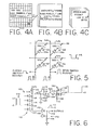
- Fig. 4 illustrates schematically a calculation to determine the size in bits required for the main memory 10 so as to drive a display unit 48 with 100 seconds of video.
- standard video produces a display which is refreshed at a rate of thirty frames a second using what is referred to as an interlaced technique.
- a black and white television display has 525 raster lines per frame, of which about 42 are blanked for retrace purposes. For each field there are 262-1/2 lines of which 21 are blanked lines.
- standard television operates on a principle of displaying a field having approximately 240 unblanked lines in 1/60 of a second, retracing the electron beam to the beginning position at the upper left and then interlacing in between the original 240 lines a second field of 240 lines.
- the original field and the interlaced field are each written onto the screen in 1/60 of a second, about 16.7 milliseconds.
- Fig. 4A schematically indicates the number of fields that must be stored to display 100 seconds of video. At 30 fields a second, each displayed in 1/60 of a second, 100 seconds requires 3,000 fields.
- Fig. 4B discloses a calculation to determine the number of bits of information which must be stored for each of the 3,000 fields. As shown in Fig. 4B, each field has 240 displayable horizontal scan lines. Each scan line has approximately 256 pixels of display locations. In a preferred embodiment, the pixels of information are digitized into 3-bit representations.
- Main memory 10 stores for repetitive read-out all of the necessary information to display 3,000 fields.
- Fig. 4C schematically shows one form of organization of the bits on the set of three memory planes or units 51a through 51c.
- each of the memory planes or units 51a through 51c is associated with one of the three bits necessary to represent each pixel.
- Each memory plane or unit 51a through 51c must contain enough storage to support 3,000 fields times 240 lines per frame times 256 pixels per line which corresponds to 1.84 x 10 8 bits.
- Such a memory plane or unit can be organized as 15,000 rows by 12,288 columns.
- the diode portion of each of the storage cells 56 through 59 has the following characteristics: area - 2 by 2 microns; maximum current density - DC 20 amps/cm 2 corresponding to .8 microamps of constant current and pulsed 100 amps/cm 2 corresponding to 4.0 microamps of pulsed current; a voltage drop of 3 volts at 4.0 microamps; and the thickness of the intrinsic region between the p and the n layers equal to .3 microns with a junction capacity of aDout .00133 picofarads.
- Retaining the 2 by 2 micron area of the diode in the switch results in the following switch characteristics when a settable material such as S i 50 C 50 disclosed in the previously identified and incorporated patent applications is used: R off is greater than 10 ohms, R on is approximately 10 ohms with a switch thickness on the order of .08 microns resulting in a parallel capacitance of .005 picofarads.
- the size of the memory units or planes 51a through 51c is on the order of 2-3/8 inches high by 2 inches wide.
- the system 5 of the present invention can readily include a main memory 10 which is portable and, in fact, holdable in one's hand.
- each field of video and audio information which is stored takes five rows of the 15,000 rows indicated.
- Fig. 5 shows a schematic diagram in more detail of a part of the memory unit 50 of Fig. 2.
- Fig. 5 also corresponds to the structure of each memory unit 51a, 51b, 51c.
- storage units 56 through 59 are indicated schematically as diodes in series with settable switches.
- the diode 56a is shown in series with the settable switch element 56b which in Fig. 5 is indicated as being in an open position.
- Storage element 57 is shown as a diode 57a in series with a closed switch element 57b. Addressing the elements 56, 57 is accomplished by applying appropriate voltages to the column lines 54a and 54b and row line 52a.
- a storage element such as 56 is uniquely selected in each corresponding memory unit 50, 51a, 51b or 51c. Read out circuitry then can be used to sense and read out the position of the switch 56b in element 56.
- the switch elements such as the element 56b, are typically formed of a settable material such as Si SO C 50 as disclosed in the above-identified patent applications. By setting the position of the switch 56b, either a 1 or a 0 can be stored in the memory cell 56.
- the memory unit 50 is a form of nonvolatile, passive storage.
- the memory unit 50 can be used as a read-only memory unit (ROM) when the settable switch elements have to be set during the fabrication process or where the settable switch elements can be set or reset only a very limited number of times.
- the memory unit 50 can be used as an electrically erasable and programmable ROM (EEPROM) where the switch elements are of a type that can be settable and resettable electrically many times.
- EEPROM electrically erasable and programmable ROM
- Fig. 6 illustrates an exemplary circuit 110 that can be used to select a desired row, select a desired column, and sense the bit of information, a 1 or a 0, stored at the selected memory cell.
- a diode AMD-gate 112 is used to select a column such as exemplary column 54b.
- the AND gate 112 includes selection diodes 114 through 120 and pull-up resistor 122.
- Column selection signals are applied to the cathodes of the diodes 114 through 120.
- An exemplary selection signal 124 is shown on Fig. 6.
- Selection signal 124 is nominally at -3 volts when a diode is not being selected and goes to +3 volts for each of the diodes 114 through 120 as they are selected.
- each of the diodes 114 through 120 must be reverse biased by a select signal such as -3 volts at a cathode thereof. In such an instance, the voltage at the node 126 attempts to rise toward a 15 volt potential through a resistor 122. Diodes 114 through 120 become forward biased when the voltage at the node 126 approaches +6 volts.
- a column shunt capacitor 128 of 20 picofarads Attached to the node 126 is a column shunt capacitor 128 of 20 picofarads.
- the 20 picofarads corresponds to estimated shunt capacitance of the column 54b.
- an anode end of the diode 56a of the storage element 56 Also as shown in Fig. 6, the switch 56b of the memory unit 56 is open indicating that a 0 is being stored at that location.
- AND gate 130 Connected to the other end of the switch 56b by means of the row 52a is a second diode AND gate 130.
- AND gate 130 includes two diodes 132 and 134 along with a resistor 136. The cathodes of the diodes 132, 134 and one end of the resistor 136 are connected together at a node 138 which in turn is connected to the row to be selected such as 52a.
- a +3 volt signal is applied to the anode of each of the diodes 132, 134. Due to the -15 volt bias at the other end of the resistor 136, the voltage at the node 138 is clamped to approximately 0 volts.
- the AND gate 112 would permit the voltage at the node 126 to rise toward a positive voltage of six volts
- the diode 56a in the storage cell 56 clamps that node at +3 volts for a closed switch 56b. In the event that switch 56b is open, the voltage at the node 126 is permitted to rise toward six volts when the diode gate 112 is enabled.
- the read-out circuit 140 includes diodes 142, 144 and load resistor 146.
- the elements 142, 144 and 146 form a diode OR gate.
- a plurality of diodes in addition to the diodes 142, 144 can be attached to the load resistor 146.
- a group of columns can be ORed together to reduce the number of read-out circuits and read-out lines that are required for the memory.
- twelve columns are ORed together in output OR gates such as the circuit 140.
- the resistor 122 has a value which is selected so that the current therethrough will not exceed 1.2 microamps.
- the 1.2 microamps is a maximum desired current which can be permitted to flow through any one of the column select diodes 114 through 120.
- the selection diodes such as 114 through 120, 132 and 134 as well as the output diodes 142, 144 all are formed on the memory plane such as 51a using the same type of amorphous silicon alloys that are used to form the memory cells such as 56. Specifically, these selection diodes, which form diode gates, may be formed in the layer 55 of amorphous silicon alloy. Resistive elements 122, 146 can be formed in a conventional fashion also on the planar substrate, or attached thereto, that supports the memory plane 51a.
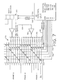
- Fig. 7 shows a more complete schematic of the row select circuitry 70c connected to the planar memory unit 51c.
- row select diodes 132, 134 and load resistor 136 are shown connected to exemplary row 52a of the memory plane 51c.
- an anode of the diode 134 is controlled by a line 150 from the control unit 20.
- the line 150 is used to select which of two frames is currently being read out from the memory plane 51c.
- An anode of the diode 132 is connected by a line 152 to a row indicator in the control unit 20.
- Row 1 of memory plane 51c has stored therein horizontal scan line information for scan lines 1 through 48 of the raster.
- An end of the load resistor 136 is connected to a line 154 and controlled through an inverter 156 to switch the diode gate 132, 134 and 136 on or off.
- the inverter 156 puts out a -15 volt signal when the gate 132, 134 and 136 is to be enabled and a +6 volt signal otherwise.
- Inverter 156 is controlled by a voltage on a line 158 which in turn is generated through a shift register 160.
- the shift register 160 is part of the control unit 20 and has a single bit which recirculates under the control of the control unit 20. The recirculating bit enables selected inverters such as 156 to enable a pair of stored frames in memory plane 51c.
- the control unit 20 generates start pulses on a line 162 and reset pulses on a line 164 to control the shift register 160.
- the additional diode gates shown on Fig. 7 are identical to the two-input AND gate with elements 132, 134, 136. Alternate frames and different rows as selected by control unit 20 are selected by the remainder of the diode gates. Since the memory plane 51c has 15,000 rows, and since these rows are selected in groups of ten by the shift register 160, shift register 160 must have a total of 1500 storage locations.
- a first field stored in memory plane 51c can be selected to be read out or a second field, depending on whether field A or field B is enabled by signals on the lines 150, 151.
- Field A and field B are arbitrary designations which merely refer to two time-adjacent non-interlaced fields which are to be displayed one after the other on the raster with an interlaced field to be displayed in time between them.
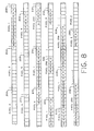
- Fig. 8 discloses a layout of the data for each group of 48 raster lines which are stored in a given row of a memory plane such as 51c.
- Fig. 9 discloses a preferred embodiment of the column select and read-out circuitry based on the data layout as shown in Fig. 8.
- Fig. 8 discloses in detail the layout of row 1 of memory plane 51c.
- the data organization for the other two memory planes 51a and 51b is identical except they correspond to different bits in the 3-bit representation of the video gray-scale signal.
- the layout of other rows in memory plane 51a is similar except that the data stored therein is for different rows of the raster or for different fields.
- row 1 of the memory plane 51c is organized with the pixels for line number 1 of the raster distributed horizontally on the row.
- Each pixel for line number 1 is twelve locations apart from each adjacent stored pixel for line 1.
- element 200 correspond to pixel 1 of line number 1.
- Element 202 corresponds to pixel 2 of line number 1.
- Elements 204 through 210 correspond to pixels 3 through 6 for line 1.
- element 212 corresponds to pixel number 256 for line 1.
- pixel 1 for line 2 which is indicated as element 214.
- elements 216 through 220 correspond to pixels 2 through 256 for line 2.
- Distributed laterally along the row from pixel 256 for line 2, number 220, is element number 222 which is pixel 1 for line 3.
- the pixel 2 through 256 for line 3 are distributed laterally along the row with element 224 corresponding to pixel 256 for line 3.
- Spaced laterally from pixel 256 of line 3 is an element 226 which is pixel 1 for line 4.
- the remaining pixels 2 through 256 for line 4 are distributed laterally along the row and are represented by numerals 228, 230 through 232.
- Fig. 9 Shown in Fig. 9 is row 1 of memory unit 51c, corresponding to the detailed diagram of Fig. 8 along with a plurality of column lines 250 which correspond to the 12,288 columns indicated in Fig. 4C.
- a line 54b corresponding to the line 54b shown in Fig. 5 as well as in Fig. 6.
- line 54b Also shown connected to line 54b is the set of four diodes 114 through 120 and load resistor 122 which form the selection AND gate 112, as indicated in Fig. 6, for the purpose of selecting each of the pixels for lines 1 through 4 which are read out as a group.
- Inputs to the cathodes of diodes 114 through 120 are generated by a set of inverters 252 through 258 whose inputs on a set of lines 260 through 268 are generated by the control unit 20 for the purpose of selecting the first group of four raster lines 1 through 4, then the second group of four raster lines 5 through 8, then the third group of four raster lines 9 through 12 all the way through the twelfth group of raster lines 45 through 48.
- lines 260 through 268 contain a 4-bit binary code which is stepped from 0 (0000) through 11 (1011).
- Shift register 280 a 1024 bit shift register, is loaded in parallel and stores 256 pixels for each of four raster lines. Shift register 280 is loaded a total of twelve times to read out the entire data contents of each row of memory plane 51c. When loaded, the 1024 bits of shift register 280 are shifted via a line 282 to the interpolator circuitry 80 for the purpose of displaying the stored fields and for generating and displaying the interlaced fields which were not stored in the main memory 10.
- circuitry shown in Fig. 9 with respect to memory unit or plane 51c would, in a preferred mode, be formed integral to the memory unit or plane 51c.
- selection diodes used for addressing may be formed in the amorphous silicon alloy layer.
- the diodes of the diode AND gates and diode OR gates may be formed in the alloy layer. All of the connections and interconnections would be made on the supporting substrate with a line such as 282 coming off of the substrate, for each of the three bits, and going to interpolator 80. While an exemplary AND gate having diodes 114 through 120 and load resistor 122 has been discussed with respect to column 54b, it will be understood that the remaining columns incorporate diode AND gates that work in precisely the same fashion as does the exemplary gate.
- Fig. 9 While the above discussion of Fig. 9 has been with respect to memory unit or plane 51c, it will be recognized that precisely the same circuitry would be used with memory units or planes 51a and 51b to generate a total of three bits in parallel along lines 282, 284 and 286 as indicated in Fig. 10.
- Fig. 10 discloses the detailed structure of the interpolator unit 80.
- Fig. 10 includes two read/write memory units 300 and 302 arbitrarily designated as Field A Store and Field B Store.
- Memory elements 300 and 302 are standard read/write types of memory elements each containing capacity to store 240 lines per frame with 256 pixels per line and three bits for each pixel corresponding to 184,320 bits.
- the interpolation process is controlled through the control unit 20 as well as decoder 304 which selects which memory 300 or 302 the incoming information along lines 282 through 286 is to be stored.
- Output from memory unit 300 along a plurality of lines 306 and output from memory unit 302 along a plurality of lines 308 is connected to a multiplexer 310.
- Multiplexer 310 can either gate the outputs along lines 306 from memory unit 300 directly to a set of output lines 312, or can gate the outputs on lines 308 from the memory unit 302 directly to the video output lines 312. Alternately multiplexer 310 can select the result of the interpolation which is performed by the parallel binary adder 314. The output sum from the adder 314 appears on a plurality of lines 316 and is gated to the video output lines 312.
- the interpolation process is performed and the result displayed as an interlaced field using stored information from the field displayed immediately before the interpolation and stored information from the field which is to be displayed immediately after the interpolation is completed.
- the information upon which the interpolation process is based is stored in the memory units 51a, 51b, 51c.
- the field which results from the interpolation is formed as the mean of the prestored pixel intensity values at each pixel location in the two fields.
- the interpolation is performed at the parallel adder 314 by addition of pixel intensity values after the values for each location are simultaneously read from the Field A Store 300 and the Field B Store 302. This process results in a four-bit quantity representing each interpolated pixel intensity as the mean of two three-bit quantities.
- This additional bit is carried through the multiplexer 310 and used in the formation of the analog video signal.
- the fourth or least significant bit is represented as a zero.
- the prestored intensity pixels are effectively multiplied by two.
- the sum on the lines 316 can be divided by two by shifting the sum one binary position to the right as required in forming a mean value.
- the sum formed in the interpolation process is a weighted sum.
- the two stored pixel intensity values that are added together are equal weight. Alternate weighting schemes could be used where more than one raster line was to be interpolated between prestored pixel intensity values.
- the first 240 line field to be displayed is transferred from the main memory 10 to the Field A Storage 300.
- the process is then started, and during the first time interval, about 16.7 milliseconds, Field A is read out from storage 300 in parallel form via lines 306 through the multiplexer 310 and onto the lines 312.
- the next 240 line field is transferred from the main memory 10 to the Field B Storage 302.
- Field A is read from storage 300 and Field B is read from storage 302 in a synchrozined manner so that the interpolation can be performed for each pixel 1.ocation to produce the interlaced field.
- Field B in storage 302 is read out in-the third 16.7 millesecond interval and the contents of Field A Storage 300 is replaced by the next field from main storage 10.
- Field A Storage 300 is read out and displayed while Field B Storage is loaded with the next field from the main storage 10. The read-out and interpolation process can continue in this manner until the contents of main memory 10 have been displayed.
- a time-varying sequence of digital information is alternately read out of the memories 300, 302 onto the lines 306, 308 at a real-time rate necessary to display an image on the unit 48.
- the rate at which information is read out of main memory 10 and into Field A Store 300 or Field B Store 302 can be equal to the real-time rate that the information is read-out from the storage units 300, 302.
- read-out from main memory 10 can be faster or slower (a first rate) than the real-time read-out rate (a second rate) from the units 300, 302.
- the read-out rate from main memory 10 to the memory units 300, 302 can be somewhat slower than the read-out rate from the units 300, 302 by taking advantage of the horizontal and vertical retrace times of the display unit 48 during which no information is displayed.
- the use of different first and second read-out rates has the advantage that, so long as the first rate is at least one-half the second rate, full advantage can be taken of the speed characteristics of the memory unit 10.
- Audio information is also stored in the main memory 10 along with the video line information. Of the 256 pixels per line, eight pixels are reserved for audio information, corresponding to 24 bits. The audio information is sampled twice during each scan line corresponding to a 31.47 kilohertz sample rate. The information from each of the two audio samples is stored in the memory 10 at the end of the video information for that line. Six bits are used to store the audio information for each sample from a given line. Additionally, the audio for each interlaced line is stored in twelve bits along with the audio for the adjacent non-interlaced line. Hence, while the video for the interlaced lines is interpolated, the audio is stored and carried along'as part of the information in main memory 10. When the information in memory 300 or 302 is read out on lines 306 or 308, respectively, and the end of a horizontal line approaches the 12 bits for the audio corresponding to that particular line are gated through multiplexer 313 to the audio decoder circuitry 96.
- Fig. 11 discloses an exemplary embodiment of the audio decoder circuitry 96.
- Audio data is gated through the multiplexer 313 onto the lines 315 and through gates 317 through 320 selectively into shift registers 322, 324 and 326.
- the capacity of the shift registers 322 through 326 is 12 bits.
- a decoder 330 is controlled through the control unit 20 to gate the 12 bits of audio information on lines 315 into the shift registers 322 through 326.
- Six bits of information are then transferred from the shift registers 322 through 326 into a 6 bit storage register 334.
- the output from register 334 on a set of lines 336 Corresponds to six bits of sampled audio which is then fed through the digital-to-analog converter 100 to create an analog audio signal on the line 45.
- the analog audio signal on the line 45 is displaced slightly in time from its sample position with respect to a given horizontal raster line.
- the first 6 bit sample was taken in the middle of the horizontal scanline and the second 6 bit sample was taken at the end of the scan line.
- the first sample is converted back into an analog signal on the line 45 at the end rather than the middle of the raster line where it was originally sampled, a delay of some 32 microseconds.
- the second sample of digitized audio is gated through digital-to-analog converter 100 in the middle of the next horizontal scan line, a delay in that sample on the order of 32 microseconds.
- the audio output on line 45 can be fed directly to a monitor 48 along with a composite video signal on the line 35.
- the sync generator 87 is a well understood element which is known in the art, as is the summing point 90 and the RF modulator 102.
- the main memory 10 would include the memory units or planes 51a, 51b and 51c.
- Each of the memory units or planes 51a, 51b and 51c would include integrated column select and read-out circuitry and row select circuitry such as the exemplary column select and read-out circuitry 74c and row select circuitry 70c, all formed a common substrate.
- the three memory units 51a, 51b, 51c, one for each bit of the video, would then be physically interconnected adjacent one another and connected via the parallel lines 282, 284, 286 to the interpolator 80 and by the lines 20a, 20b to the cantrol unit 20. All of the remaining circuitry such as the control unit 20, clock 106, video signal formation circuitry 30 and audio signal formation circuitry 40 could be integrated with the memory planes 51a, 51b and 51c.
- the broader aspects of the invention include storing and reading-out at a selected frequency additional bits of information associated with a gray-scale of higher resolution or the luminance, hue and saturation components of color such that a raster scan color display could be stored and presented in real-time.
- the broader aspects of the invention include the use of additional digital or analog processing of the video gray-scale signal generated by the interpolator circuitry so as to improve the quality of the displayed images.
- the broader aspects also include the use of any established method of coding the bits representing each pixel, each line or an entire field for storage in the main memory with the limitation that it will be necessary to decode the information to a linear or other continuous representation of each pixel intensity value before the interpolation process is performed. It is also within the broader aspects of this invention to interpolate more than one intermediate field between each pair of stored fields by weighting the pixel intensity values from each stored image according to the position of the field being created within the time interval over which the interpolation is performed.
- the broader aspects of the invention also include taking advantage of the retrace characteristics of the display unit to be used so that read-out from main memory can take place at a first rate different from a second rate of read-out from the interpolation unit.
- the broader aspects of the invention include storing in the main memory digital information directed to any desired application.
Landscapes
- Engineering & Computer Science (AREA)
- Multimedia (AREA)
- Signal Processing (AREA)
- Computer Networks & Wireless Communication (AREA)
- General Engineering & Computer Science (AREA)
- Television Systems (AREA)
- Transforming Electric Information Into Light Information (AREA)
- Control Of Indicators Other Than Cathode Ray Tubes (AREA)
- Read Only Memory (AREA)
Applications Claiming Priority (2)
| Application Number | Priority Date | Filing Date | Title |
|---|---|---|---|
| US06/678,165 US4679085A (en) | 1984-12-04 | 1984-12-04 | Digital integrated electronic storage system for video and audio playback |
| US678165 | 2007-02-23 |
Publications (2)
| Publication Number | Publication Date |
|---|---|
| EP0184138A2 true EP0184138A2 (de) | 1986-06-11 |
| EP0184138A3 EP0184138A3 (de) | 1988-09-07 |
Family
ID=24721667
Family Applications (1)
| Application Number | Title | Priority Date | Filing Date |
|---|---|---|---|
| EP85115092A Withdrawn EP0184138A3 (de) | 1984-12-04 | 1985-11-28 | Anzeigesystem |
Country Status (3)
| Country | Link |
|---|---|
| US (1) | US4679085A (de) |
| EP (1) | EP0184138A3 (de) |
| JP (1) | JPS61139999A (de) |
Cited By (4)
| Publication number | Priority date | Publication date | Assignee | Title |
|---|---|---|---|---|
| GB2223645A (en) * | 1988-09-13 | 1990-04-11 | Asahi Optical Co Ltd | Still video system in which an audio signal previously stored in a memory can be reproduced |
| EP0374285A1 (de) * | 1988-12-21 | 1990-06-27 | Deutsche ITT Industries GmbH | Tragbare elektronische Bildaufnahmeeinrichtung |
| WO1991007053A3 (en) * | 1989-11-02 | 1991-06-27 | Eastman Kodak Co | Pre-event/post-event recording in a solid state fast frame recorder |
| EP0370064A4 (en) * | 1987-07-27 | 1993-02-10 | David Geshwind | A method for transmitting high-definition television over low-bandwidth channels |
Families Citing this family (17)
| Publication number | Priority date | Publication date | Assignee | Title |
|---|---|---|---|---|
| JPS61235981A (ja) * | 1985-04-12 | 1986-10-21 | Toshiba Corp | プレゼンテ−シヨン装置 |
| US4864613A (en) * | 1986-11-10 | 1989-09-05 | General Instrument Corporation | Broadband converter/descrambler interface for cable TV |
| US4821097A (en) * | 1987-03-05 | 1989-04-11 | General Instrument Corporation | Apparatus and method for providing digital audio on the sound carrier of a standard television signal |
| KR920001287B1 (ko) * | 1988-02-12 | 1992-02-10 | 니혼 호오소오 고오카이 | 디지탈 영상신호 처리장치 |
| US5159661A (en) * | 1990-10-05 | 1992-10-27 | Energy Conversion Devices, Inc. | Vertically interconnected parallel distributed processor |
| GB9117680D0 (en) * | 1991-08-16 | 1991-10-02 | Philips Electronic Associated | Electronic matrix array devices |
| DE4229710B4 (de) * | 1991-09-09 | 2008-06-05 | Samsung Electronics Co., Ltd. | Digitales Audiodatenspeicherungssystem und damit ausgerüstetes digitales Audio-System |
| US5657423A (en) * | 1993-02-22 | 1997-08-12 | Texas Instruments Incorporated | Hardware filter circuit and address circuitry for MPEG encoded data |
| US5628031A (en) * | 1993-07-19 | 1997-05-06 | Elonex Ip Holdings Ltd. | Personal digital assistant module implemented as a low-profile printed circuit assembly having a rigid substrate wherein IC devices are mounted within openings wholly between opposite plane surfaces of the rigid substrate |
| US5642171A (en) * | 1994-06-08 | 1997-06-24 | Dell Usa, L.P. | Method and apparatus for synchronizing audio and video data streams in a multimedia system |
| US6836295B1 (en) | 1995-12-07 | 2004-12-28 | J. Carl Cooper | Audio to video timing measurement for MPEG type television systems |
| US5920499A (en) * | 1997-01-02 | 1999-07-06 | United Microelectronics Corp. | Method of decoding a diode type read only memory |
| US5987525A (en) * | 1997-04-15 | 1999-11-16 | Cddb, Inc. | Network delivery of interactive entertainment synchronized to playback of audio recordings |
| US20020102092A1 (en) * | 2001-01-31 | 2002-08-01 | Sony Corporation And Sony Electronics Inc. | RF passthrough for digital network recorders |
| US6917349B2 (en) * | 2001-02-28 | 2005-07-12 | Intel Corporation | Displaying information on passive storage medium |
| CA2380884C (en) * | 2002-04-08 | 2006-01-10 | Leitch Technology Corporation | Method and apparatus for representation of video and audio signals on a low-resolution display |
| GB2433647B (en) * | 2005-12-20 | 2008-05-28 | Univ Southampton | Phase change memory materials, devices and methods |
Family Cites Families (5)
| Publication number | Priority date | Publication date | Assignee | Title |
|---|---|---|---|---|
| JPS5694589A (en) * | 1979-12-27 | 1981-07-31 | Nec Corp | Memory device |
| US4347585A (en) * | 1980-06-09 | 1982-08-31 | International Business Machines Corporation | Reproduce only storage matrix |
| GB2119606B (en) * | 1982-01-09 | 1985-07-10 | Imp Computers Limited | Improvements in and relating to television type displays |
| US4677742A (en) * | 1983-01-18 | 1987-07-07 | Energy Conversion Devices, Inc. | Electronic matrix arrays and method for making the same |
| US4545111A (en) * | 1983-01-18 | 1985-10-08 | Energy Conversion Devices, Inc. | Method for making, parallel preprogramming or field programming of electronic matrix arrays |
-
1984
- 1984-12-04 US US06/678,165 patent/US4679085A/en not_active Expired - Lifetime
-
1985
- 1985-11-28 EP EP85115092A patent/EP0184138A3/de not_active Withdrawn
- 1985-12-03 JP JP60272361A patent/JPS61139999A/ja active Pending
Cited By (7)
| Publication number | Priority date | Publication date | Assignee | Title |
|---|---|---|---|---|
| EP0370064A4 (en) * | 1987-07-27 | 1993-02-10 | David Geshwind | A method for transmitting high-definition television over low-bandwidth channels |
| GB2223645A (en) * | 1988-09-13 | 1990-04-11 | Asahi Optical Co Ltd | Still video system in which an audio signal previously stored in a memory can be reproduced |
| GB2223645B (en) * | 1988-09-13 | 1993-04-21 | Asahi Optical Co Ltd | Still video system in which an audio signal previously stored in a memory can be reproduced |
| EP0374285A1 (de) * | 1988-12-21 | 1990-06-27 | Deutsche ITT Industries GmbH | Tragbare elektronische Bildaufnahmeeinrichtung |
| US5077612A (en) * | 1988-12-21 | 1991-12-31 | Deutsche Itt Industries Gmbh | Portable electronic picture recording device with nonvolatile electronic memory |
| WO1991007053A3 (en) * | 1989-11-02 | 1991-06-27 | Eastman Kodak Co | Pre-event/post-event recording in a solid state fast frame recorder |
| US5140436A (en) * | 1989-11-02 | 1992-08-18 | Eastman Kodak Company | Pre-event/post-event recording in a solid state fast frame recorder |
Also Published As
| Publication number | Publication date |
|---|---|
| JPS61139999A (ja) | 1986-06-27 |
| EP0184138A3 (de) | 1988-09-07 |
| US4679085A (en) | 1987-07-07 |
Similar Documents
| Publication | Publication Date | Title |
|---|---|---|
| US4679085A (en) | Digital integrated electronic storage system for video and audio playback | |
| US4630122A (en) | Television receiver with liquid crystal matrix display panel | |
| US4870399A (en) | Apparatus for addressing active displays | |
| US4339775A (en) | Fast frame rate augmentation | |
| US4847809A (en) | Image memory having standard dynamic RAM chips | |
| EP0216188B1 (de) | Rasteranzeigetafel | |
| US4210934A (en) | Video display apparatus having a flat X-Y matrix display panel | |
| US4369504A (en) | Serial-parallel signal converter | |
| NL8301566A (nl) | Inrichting voor het maken van een foto-, diarespektievelijk filmafbeelding van een televisiebeeld. | |
| JPH07118794B2 (ja) | 表示装置 | |
| JPH0681304B2 (ja) | 方式変換装置 | |
| JP4727038B2 (ja) | 隣接した列のグループ内を交互走査制御されるマトリクスディスプレイスクリーンへの表示方法 | |
| US4890101A (en) | Apparatus for addressing active displays | |
| US4233602A (en) | Multi-matrix display system having matrix display panel with uncrossed connections on substrates | |
| EP0319291B1 (de) | Anzeigegerät | |
| JPS6186784A (ja) | エレクトロスコープ画像表示装置 | |
| US5172242A (en) | Visual presentation system employing two or more video disk players for providing as many correlated images | |
| US5990974A (en) | Video signal processing apparatus | |
| US4558362A (en) | Digital video signal transmitting apparatus | |
| US5394286A (en) | Method for the addressing of elementary heads of a multipack head for recording on a magnetic medium, and magnetic head implementing said method | |
| JP2501101B2 (ja) | 画像メモリ | |
| CA1169961A (en) | Apparatus for storing signals | |
| JP3015544B2 (ja) | 液晶表示装置 | |
| JP2768361B2 (ja) | 画像フレームメモリのデータ入出力方式 | |
| JPH0126226B2 (de) |
Legal Events
| Date | Code | Title | Description |
|---|---|---|---|
| PUAI | Public reference made under article 153(3) epc to a published international application that has entered the european phase |
Free format text: ORIGINAL CODE: 0009012 |
|
| AK | Designated contracting states |
Kind code of ref document: A2 Designated state(s): DE FR GB IT NL SE |
|
| PUAL | Search report despatched |
Free format text: ORIGINAL CODE: 0009013 |
|
| AK | Designated contracting states |
Kind code of ref document: A3 Designated state(s): DE FR GB IT NL SE |
|
| STAA | Information on the status of an ep patent application or granted ep patent |
Free format text: STATUS: THE APPLICATION IS DEEMED TO BE WITHDRAWN |
|
| 18D | Application deemed to be withdrawn |
Effective date: 19890308 |
|
| RIN1 | Information on inventor provided before grant (corrected) |
Inventor name: CHAPELLE, WALTER E. Inventor name: JOHNSON, ROBERT R. |